


Hardware components | ||||||
| × | 1 | ||||
| × | 1 | ||||
| × | 1 | ||||
| × | 1 | ||||
 |
| × | 1 | |||
Software apps and online services | ||||||
| ||||||
 |
| |||||
Hand tools and fabrication machines | ||||||
 |
| |||||
The ADRV9009 is a high-performance RF transceiver capable of simultaneous high-speed ADC and DAC operation, commonly used for radar, communications, and signal intelligence applications. Analog Devices provides an HDL reference design for the ZCU102 FPGA platform, which sets up the JESD204 links, RX/TX paths, and DMA streaming for rapid system bring-up.
While the reference design is fully functional, it is primarily designed to stream data to DDR memory via AXI DMA. There is no built-in mechanism to directly route ADC samples to the DAC internally, which can make quick verification of the end-to-end RF signal path cumbersome.
This project demonstrates a minimal modification to the ADI HDL reference design to implement a real-time internal digital ADC-to-DAC loopback. By connecting the ADC data stream directly to the DAC input path within the FPGA fabric:
- No external cabling or memory buffering is required.
- Engineers can verify the RX → TX chain immediately
- The internal data flow of the ADRV9009 reference design is made explicit, providing a foundation for learning and experimentation.
This tutorial focuses on identifying the relevant ADC and DAC signals, rerouting them for loopback, and verifying correct operation, giving readers a hands-on understanding of FPGA-based RF data paths.
2. Problem StatementThe official ADRV9009 HDL reference design is optimized for streaming ADC and DAC data through DDR memory via AXI DMA. While this is suitable for many applications, it does not provide a direct internal digital loopback, meaning:
- ADC samples are sent to memory (or to software) before being replayed to the DAC.
- There is no built-in path for routing ADC data directly to DAC in real time.
- Engineers cannot quickly verify the end-to-end RX → TX chain without either:
- Capturing data externally and retransmitting, or
- Using software loops, which introduces latency and complexity.
This gap creates a need for a minimal, FPGA-only loopback solution, which allows for:
- Immediate testing of the receive/transmit chain.
- Avoiding unnecessary memory transfers.
- Demonstrating the internal data flow in the ADI reference design for learning or debugging.
Why this matters:Understanding and implementing a direct ADC → DAC path is a foundational skill for FPGA-based RF systems. It allows engineers to verify signal integrity, latency, and JESD204 alignment, and forms a basis for more advanced applications like digital filtering or real-time signal processing.
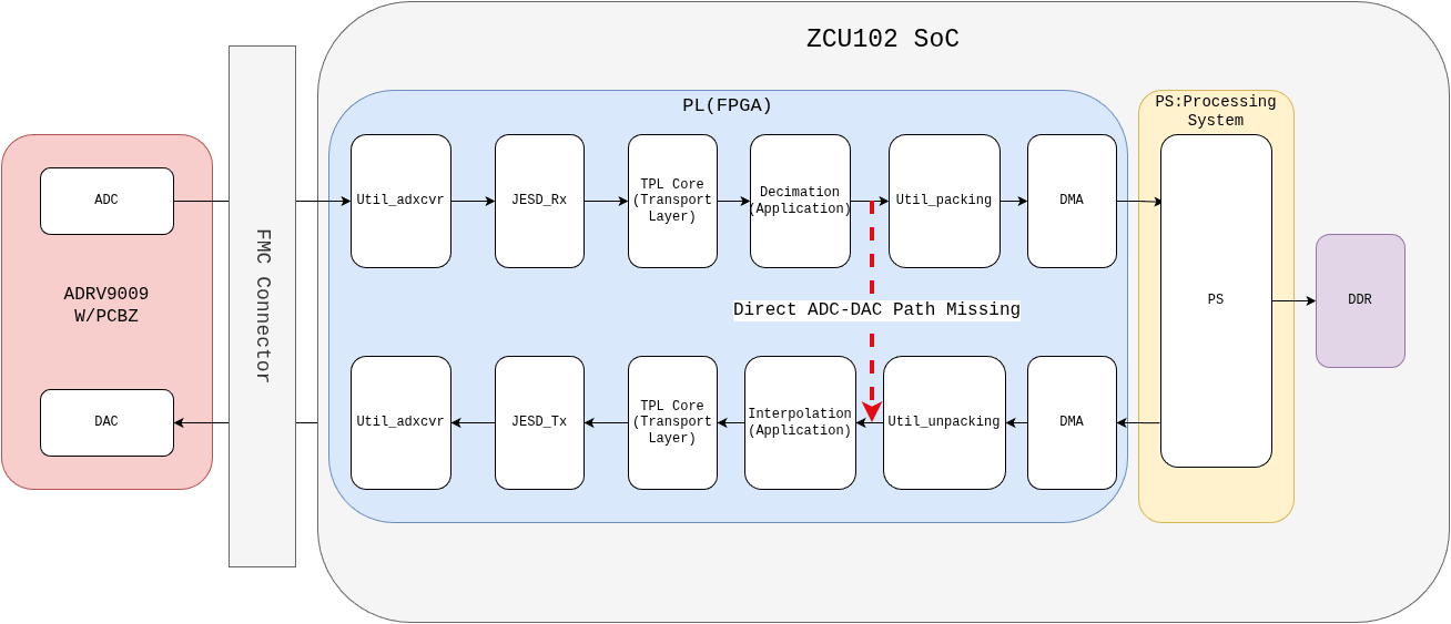
Figure 1 illustrates the motivation for the digital loopback. The dark black arrows show the default reference design path, where ADC samples go through AXI DMA and DDR memory before reaching the DAC. The dashed red arrow indicates the direct ADC-to-DAC path that does not exist in the reference design.
This project uses the following hardware and tools, and assumes a few prerequisites to ensure a smooth tutorial experience.
Hardware
- ADRV9009 W/PCBZ (Radio Verse)Evaluation BoardHigh-performance RF transceiver with dual ADC/DAC.
- Xilinx ZCU102 FPGA BoardHosts the HDL reference design and provides FPGA fabric for digital processing.
- Optional RF cables or SMA connectors (for verification, if using external signals).
- Spectrum Analyzer (I am using FieldFox Microwave Analyzer)
- Signal Source (I am using SynthUSB3 with laptop)
Tools
- Vivado Design Suite (2024.2 or compatible)For building, synthesizing, and programming the HDL reference design.
- Vitis / No-OS SDKMinimal software setup to configure ADRV9009
Prerequisites
Before following this tutorial, readers should have:
- A working ADRV9009 + ZCU102 reference design.
For this refer to my other hackster tutorial:
https://www.hackster.io/saqibsherawan/signal-transmission-and-reception-using-adrv9009-zcu102-b4d7aa
- Basic familiarity with Vivado block designs and HDL signals.
- Minimal experience with AXI DMA / FPGA I/O streaming.
The Analog Devices HDL reference design for ADRV9009 on ZCU102 provides a complete framework for bringing up the RF transceiver, JESD204B/C links, and FPGA data paths. The design is structured around separate receive (RX) and transmit (TX) chains, each optimized for high-throughput streaming using AXI infrastructure.
Receive SideOn the receive side, digitized samples from the ADRV9009 ADCs are transferred to the FPGA through:
1.util_adxcvr IP: which uses Gigabit transceivers in the background to handle huge bandwidth of data coming over JESD protocol.
2. JESD_Rx IP: Responsible for JESD204B/C protocol handling, including scrambling/descrambling, lane alignment, character replacement and alignment monitoring.
3. RX_TPL_Core IP: This IP core is used for extraction of Payload(samples) from the JESD fromat into serial stream. Transport layer peripherals are responsible for converter specific data framing and de-framing.
4. Decimation: Before this IP the data is ready for application layer, this IP in reference design is application layer from here data flows into util_cpack IP.
5. Util_cpack: This IP is a utility IP which packs the samples from both Receive channels to be sent over DMA to DDR.
6. DMA IP: This IP receives serial packed data from util_cpack and transfer to DDR through PS involvement.
At the end data is available at DMA and can be easily sent to DDR using PS. Same flow is shown in Figure 7
On the transmit side, the same process is followed in the opposite direction. Baseband samples are first stored in DDR memory and then streamed into the FPGA fabric using an AXI DAC DMA. The data is received by the ADI offload and control logic and passed to the util_dac_unpack block, where the samples are unpacked and aligned.
The unpacked data is then forwarded to the transport (TPL) core, which formats the samples into the JESD204-compliant data structure. Finally, the JESD204 TX core encodes the data and sends it through the util_adxcvr block, which handles the interface to the physical transceiver layer before the samples reach the ADRV9009 DACs. Same flow is shown in Figure 8
To implement an internal digital loopback, it is essential to understand exactly where ADC samples become available in the FPGA fabric and where DAC samples are expected by the transmit chain. This section focuses on identifying those tap points in the ADI reference design.
Receive SideOn the receive I/Q data is available immediately after rx_adrv9009_tpl_core. The table in Figure 9 shows which data correspond to which receiver. Figure 10 shows exactly where data is available and where it is routed (rx_fir_decimation_core)
On the transmit side the tx_adrv9009_tpl_core expects 4 parallel streams of I/Q data as listed in table of Figure 11.
The core that excepts this data is shown in Figure 12
As you can see in table above the transmit side expects two consecutive samples in parallell. And on the receive side you are getting one sample per clock for both channels. The receive side has 2 JESD lanes and the trasnmit side has 4 but the data rate is matched because the the tx side clock is half the receive side clock. This whole concept is elaborated in below section.
6. Understanding ADC-DAC Internal Loopback: Data Handling, JESD Lanes, and Clock MatchingIn this tutorial section, we'll dive deep into the concept of internal loopback between an Analog-to-Digital Converter (ADC) and a Digital-to-Analog Converter (DAC), with a specific focus on how data is processed on the transmit (TX) and receive (RX) sides. This is particularly relevant in high-speed data converter systems, such as those using the JESD204B/C interface standard, commonly found in RF systems, software-defined radios, and FPGA-based designs (e.g., Xilinx RFSoC or Analog Devices transceivers). The internal loopback allows for testing and validation by routing digital data from the ADC output directly back to the DAC input within the device, bypassing external analog paths. This helps in verifying signal integrity, synchronization, and data flow without needing external hardware.
The above section 5. ADC and DAC Data Path Analysis summary highlights a key asymmetry in how data is handled between the TX (DAC) and RX (ADC) sides, including differences in parallelism, JESD lanes, and clock rates. We'll break this down step by step, starting with foundational concepts, then exploring the TX and RX sides in detail, and finally explaining how the data rates are balanced despite these differences. We'll use tables to illustrate data formats and timing, and incorporate diagrams for visual clarity.
Basics of JESD204 Interface in ADC-DAC Systems
The JESD204 standard (evolutions like JESD204B and JESD204C) is a high-speed serial interface for connecting data converters (ADCs and DACs) to logic devices like FPGAs or ASICs. It replaces older parallel interfaces (e.g., LVDS) with serialized lanes to reduce pin count, improve noise immunity, and support multi-gigabit data rates.
Key Parameters in JESD204:
- L (Lanes): Number of serial lanes per link.
- M (Converters): Number of ADCs or DACs per device.
- S (Samples per Frame): Number of samples sent per converter per frame cycle.
- F (Frames per Multiframe): Grouping of frames for alignment.
- N' (Octet Width): Effective bit width per sample (after encoding).
- Line Rate: The serial data rate per lane, typically in Gbps.
- Device Clock and Lane Clock: The device clock drives the converter sampling, while the lane clock (derived from it) handles serialization.
In an internal loopback mode, the digital data captured by the ADC is fed directly to the DAC internally. However, the interface to the host (e.g., FPGA) still uses JESD lanes for configuration and monitoring. The asymmetry arises because ADCs and DACs may operate at different effective sample rates or with different interpolation/decimation factors, leading to varied data packing and clocking needs.
For visualization, here's a typical JESD204 interface setup between an ADC/DAC and an FPGA:
The Transmit Side (DAC): Handling Two Consecutive Samples in Parallel
On the transmit side, which refers to the DAC input interface, the system expects data in a specific format to match the converter's processing capabilities. In many configurations, especially with interpolation (where the DAC upsamples data), the input data is provided in parallel to efficiently feed the converter at high speeds.
Parallel Sample Input Explained:
- The DAC often requires "two consecutive samples in parallel" per clock cycle. This means that for each clock tick, the interface accepts two samples simultaneously—one for the current time step and one for the next—typically for complex data (I/Q channels in RF applications).
- Why parallel? This reduces the required clock frequency for the digital interface while maintaining high throughput. For example, if the DAC samples at 2 GSPS (giga-samples per second), but the input clock is slower, parallelism doubles the effective data ingestion rate.
- In JESD204 terms, this ties into the transport layer, where samples are mapped into octets and frames. For a DAC with interpolation factor of 2, the input data rate is half the output sample rate, but parallelism ensures no bottleneck.
Note:Table in Figure 11 exactly maps the format
The Receive Side (ADC): One Sample per Clock for Both Channels
In contrast, the receive side (ADC output interface) delivers data more sequentially. Here, you get "one sample per clock for both channels, " meaning each clock cycle outputs a single sample pair (one for each channel, e.g., I and Q).
Sequential Sample Output Explained:
- The ADC captures analog signals and converts them to digital at a high sample rate, often with decimation to reduce data volume.
- "One sample per clock for both channels" implies that per device clock, the interface provides one sample from channel 1 and one from channel 2 simultaneously, but without the parallelism seen on TX. This is common in decimated modes where the output rate is lower than the raw ADC rate.
- For example, if the ADC samples at 4 GSPS but decimates by 4, the output is 1 GSPS, delivered one sample per clock.
- In JESD204, this data is then packed into frames and sent over lanes. With fewer lanes (2 in this case), the serialization must be efficient to avoid overflow.
Section 6 and 7 elaborate in length how data is available from ADC and DAC. To acheive the internal loop back we need to re format the data and increase the data for DAC.
Step 1: Identification of point for Data Tapping (Receive Side)
The receive-side data is tapped after the util_adrv9009_rx_cpack block, as shown in Figure 14. This block outputs packed and aligned ADC samples, making it a suitable point for internal digital loopback.
The exact signal used for tapping the receive data is:
packed_fifo_wr_data[63:0]This 64-bit bus contains one complex sample per channel per clock and represents the receive-side baseband data before it is forwarded to the AXI ADC DMA.
Step 2: Increasing the amount of Data and Handling Clock Domain Crossing
Next, as discussed earlier, the transmit side expects more data per clock while operating at a slower clock rate. To bridge this mismatch, two problems must be addressed:
- Store receive-side data until enough samples are available
- Handle clock domain crossing (CDC) between RX and TX clock
Fortunately, both problems can be solved in one clean shot by using the AMD Vivado built-in LogiCORE FIFO Generator IP.
The FIFO naturally:
- Buffers incoming RX samples
- Accumulates multiple samples for the TX side
- Safely handles CDC between different clock domains
In other words, instead of manually reinventing buffering and CDC logic (and debugging it at 3 AM), we let the FIFO do what it does best—quietly keep our data and our sanity intact.
Follow below Instructions exactly (elaborated through Figures to acheive this)
(Ⅰ) Press CTRL+I this will open the IP menu from here search and add FIFO Generator to the block diagram.
(Ⅱ) Next Double click the IP and Confgure it according to Figures below
At this point Click Ok and our FIFO Generator is ready for storing data and handling CDC.
Step 3: Connecting Receive Side
Now as identified earlier the tapping point is util_adrv9009_rx_cpack IP and the exact signal is named packed_fifo_wr_data[63:0].
(Ⅰ) Click on plus sign of packed_fifo_wr bus (util_adrv9009_rx_cpack) and extend it do the same for FIFO_WRITE bus (fifo_generator_ip) plus sign and extend it. Make the connections according to Figure 18.
(ⅠⅠ) Bind the write enable signal of FIFO_WRITE bus (fifo_generator) to a constant of value 1 (constant can be added to vivado in similar fashion as any other IP, CTRL+I-->Search Constant--> Double Click Constant). Follow Figure 19 & 20.
At this point our receive side is done lets move to transmit side
Step 4: Formatting Data
If you extend the FIFO read data bus of the FIFO Generator IP, you will see a signal named:
dout[127:0]At first glance, this appears to be exactly the amount of data required by the transmit side. However, do not get too excited just yet.
The FIFO Generator stacks incoming data in a specific order:
- The 64-bit word that arrives first is placed in the most significant bits (MSB)
- The 64-bit word that arrives second is placed in the least significant bits (LSB)
⚠️⚠️⚠️Very Important: Unfortunately, the transmit side expects the opposite ordering.If this data is forwarded to the TX path without correcting the order, the DAC output will exhibit spurs at multiples of the DAC clock frequency. At that point, you may spend weeks questioning your JESD configuration, clocking, and even your life choices—speaking from experience.
Figure 21 shows the FIFO Generator data storage format as documented in the AMD Vivado FIFO Generator IP documentation and explains this MSB/LSB ordering behavior.
(Ⅰ) To handle this we will be using classic slice and concat blocks. Add two slice IPs and one concat IP and configure them as shown in figures below.
(ⅠⅠ) Now make the connections according to Figure 25. Connect xlslice_0 to in0 of concat block and xl_slice_1 to in1 of the concat block. Since concat block places input at in0 in LSB this solves our problem. Also tie rd_enable to 1
Step 5: Feeding DATA to DAC Side
(Ⅰ) For this lets identify the data feeding side. We will feed our 128 bit data the output of concat to util_adrv9009_tx_unpack (specifically at s_axis_tdata signal of s_axis Bus)IP core as shown in Figure 26.
(ⅠⅠ) For this lets first delete all the cores that are bringing data to this IP in reference design which includes
(a) adrv9009_data_offload
(b) axi_adrv9009_tx_dma
Delete Both these IPs along with the interconnect that was used to mount DMA to PS.
(ⅠⅠⅠ) Make the connections according to below Figure.
Step 6: Bitstream Generation & Exporting.xsa
(Ⅰ) At this point all the modifications are complete vaildate the design. It should show success and generate bitstream.
(ⅠⅠ) Now export the.xsa file and select option of include bitstream
File-->Export-->Export Hardware-->include bitstream
Note: At this point our PL design is ready now we need to cater for the PS side.
8. Building No-OS (Baremetal) Software ApplicationStep 1: Build the Software Application Using Vitis
After generating the hardware description file (.xsa) from the HDL project, the next step is to develop the software application that will run on the Zynq Processing System (PS) of the ZCU102 board. This is done using Xilinx Vitis, the unified software development platform for embedded applications.
To begin, we will set up the no-OS (no operating system) software framework provided by Analog Devices, which contains reference software drivers and example projects tailored for their hardware platforms.
git clone --recursive https://github.com/analogdevicesinc/no-OSStep 2: Configure the Vitis Environment and Prepare for Software Build
To successfully build the software application using Xilinx Vitis, it is essential to ensure that the Vitis toolchain is correctly configured in your system environment.
2.1 Ensure Vitis is Accessible from the Command Line
Depending on your operating system, the process of setting up Vitis in your environment differs:
- On Windows:If Vitis is not automatically added to your system’s
PATH, you will need to manually add it via the System Environment Variables. This allows Vitis commands to be recognized from any terminal or command prompt. - On Linux:You can source the Vitis environment setup script directly. This script configures all the necessary environment variables to enable the use of Vitis tools in your current terminal session. Run the following command:
source /path/to/xilinx/Vitis/2024.2/settings64.shReplace /path/to/xilinx with the actual installation path where Vitis is installed on your system.
2.2 Copy the Hardware Description File (.xsa)
Next, copy the.xsa file generated in last section (from the HDL build process) into the appropriate project directory within the no-OS repository. This.xsa file will be used as the hardware platform during the software build in Vitis.
For Example:
cp /path/to/hdl/projects/adrv9009/zcu102/adrv9009_zcu102.sdk/system_top.xsa ~/adi/no-OS/projects/adrv9009/Make sure to adjust the path to match the location of your .xsa file and cloned no-OS repository.
Step 3: Building the Software Project
With the .xsa hardware description file in place and the Vitis environment properly configured, you are now ready to build the software application for the ADRV9009 + ZCU102 setup using the no-OS framework.
3.1 Navigate to the Project Directory
Change directory to the project folder where you previously copied the .xsa file:
cd ~/adi/no-OS/projects/adrv90093.2 Run the Build Commands
Execute the following commands to build the project:
# Clean any previous build artifacts (optional but recommended)
make clean

# Build the project using the Vitis toolchain
make
Now our project has been successfully build both on hardware and software side.
Step 4: Launching and Modifying the Vitis Project
After successfully building the software using the Makefile, the next step is to launch the Vitis IDE to inspect and modify the application code before deploying it to the hardware.
4.1 Launch Vitis
- Open Vitis Classic (or the standard Vitis IDE if you're not using the classic version).
- When prompted to select a workspace, choose the following directory:
~/adi/no-OS/projects/adrv9009/build- Do not create a new application project when prompted. Simply close the "Create Application Project" wizard.
Vitis will automatically detect the existing project files and metadata within the selected workspace directory.
4.2 Understanding and Modifying the Application
The default reference design included in the no-OS project is configured primarily for transmission (Tx) os samples from DDR and storing of Received samples in DDR.
To extend the functionality of the application to acheive adc-dac internal loopback we need to modify our main file and device configuration file. The files include:
1. headless.c (app/adrv9009/src)
2. talsie_config.c (app/adrv9009/profiles)
3. talise_config_ad9528.h (app/adrv9009/profiles)
These files are responsible for:
- Initializing system peripherals
- Configuring the ADRV9009 transceiver
In our case modification were made to headless.c for:
- Initalization only
My version of headless.c is as below:
// Custom Design Includes
#include "xparameters.h"

// Must Includes
#include <stdio.h>
#include "adi_hal.h"
#include "no_os_spi.h"
#include "no_os_error.h"
#include "no_os_delay.h"
#include "parameters.h"
#include "no_os_util.h"
#include "axi_dac_core.h"
#include "axi_adc_core.h"
#include "axi_dmac.h"
#ifndef ALTERA_PLATFORM
#include "xil_cache.h"
#include "xilinx_gpio.h"
#include "xilinx_spi.h"
#else
#include "altera_spi.h"
#include "altera_gpio.h"
#endif
#include "talise.h"
#include "talise_config.h"
#include "app_config.h"
#include "app_clocking.h"
#include "app_jesd.h"
#include "app_transceiver.h"
#include "app_talise.h"
#include "ad9528.h"
#include "xuartps.h"


/************************Main Function**********************************/
/**********************************************************/

int main(void)
{
    adiHalErr_t err;
    int status;

    // Compute the lane rate from profile settings
    uint32_t rx_lane_rate_khz = talInit.rx.rxProfile.rxOutputRate_kHz *
                                talInit.jesd204Settings.framerA.M * (20 /
                                no_os_hweight8(talInit.jesd204Settings.framerA.serializerLanesEnabled));
    uint32_t rx_div40_rate_hz = rx_lane_rate_khz * (1000 / 40);
    uint32_t tx_lane_rate_khz = talInit.tx.txProfile.txInputRate_kHz *
                                talInit.jesd204Settings.deframerA.M * (20 /
                                no_os_hweight8(talInit.jesd204Settings.deframerA.deserializerLanesEnabled));
    uint32_t tx_div40_rate_hz = tx_lane_rate_khz * (1000 / 40);
    uint32_t rx_os_lane_rate_khz = talInit.obsRx.orxProfile.orxOutputRate_kHz *
                                   talInit.jesd204Settings.framerB.M * (20 /
                                   no_os_hweight8(talInit.jesd204Settings.framerB.serializerLanesEnabled));
    uint32_t rx_os_div40_rate_hz = rx_os_lane_rate_khz * (1000 / 40);

    // Compute the local multiframe clock
    uint32_t rx_lmfc_rate = (rx_lane_rate_khz * 100) /
                            (talInit.jesd204Settings.framerA.K * talInit.jesd204Settings.framerA.F);
    uint32_t tx_lmfc_rate = (tx_lane_rate_khz * 100) /
                            (talInit.jesd204Settings.deframerA.K * 2 * talInit.jesd204Settings.deframerA.M /
                            no_os_hweight8(talInit.jesd204Settings.deframerA.deserializerLanesEnabled));
    uint32_t rx_os_lmfc_rate = (rx_os_lane_rate_khz * 100) /
                               (talInit.jesd204Settings.framerB.K * talInit.jesd204Settings.framerB.F);

    uint32_t lmfc_rate = no_os_min(rx_lmfc_rate, rx_os_lmfc_rate);
    lmfc_rate = no_os_min(tx_lmfc_rate, lmfc_rate);

    struct axi_adc_init rx_adc_init = {
        "rx_adc",
        RX_CORE_BASEADDR,
        TALISE_NUM_CHANNELS
    };
    struct axi_adc *rx_adc;

   struct axi_adc_init rx_os_adc_init = {
        "rx_os_adc",
        RX_OS_CORE_BASEADDR,
        TALISE_NUM_CHANNELS / 2
    };
    struct axi_adc *rx_os_adc;*/

    struct axi_dac_init tx_dac_init = {
        "tx_dac",
        TX_CORE_BASEADDR,
        TALISE_NUM_CHANNELS,
        NULL,
        3
    };
    struct axi_dac *tx_dac;

#ifdef DMA_EXAMPLE
    struct no_os_gpio_desc *gpio_plddrbypass;
    struct no_os_gpio_init_param gpio_init_plddrbypass;
    extern const uint32_t sine_lut_iq[1024];
#endif
#ifndef ALTERA_PLATFORM
    struct xil_spi_init_param hal_spi_param = {
#ifdef PLATFORM_MB
        .type = SPI_PL,
#else
        .type = SPI_PS,
#endif
        .flags = SPI_CS_DECODE
    };
    struct xil_gpio_init_param hal_gpio_param = {
#ifdef PLATFORM_MB
        .type = GPIO_PL,
#else
        .type = GPIO_PS,
#endif
        .device_id = GPIO_DEVICE_ID
    };
#else
    struct altera_spi_init_param hal_spi_param = {
        .type = NIOS_II_SPI,
        .base_address = SPI_BASEADDR
    };
    struct altera_gpio_init_param hal_gpio_param = {
        .type = NIOS_II_GPIO,
        .device_id = 0,
        .base_address = GPIO_BASEADDR
    };
    hal.extra_gpio = &hal_gpio_param;
#endif
    int t;
    struct adi_hal hal[TALISE_DEVICE_ID_MAX];
    taliseDevice_t tal[TALISE_DEVICE_ID_MAX];
    for (t = TALISE_A; t < TALISE_DEVICE_ID_MAX; t++) {
        hal[t].extra_gpio = &hal_gpio_param;
        hal[t].extra_spi = &hal_spi_param;
        tal[t].devHalInfo = (void *) &hal[t];
    }
    hal[TALISE_A].gpio_adrv_resetb_num = TRX_A_RESETB_GPIO;
    hal[TALISE_A].spi_adrv_csn = ADRV_CS;
#if defined(ZU11EG) || defined(FMCOMMS8_ZCU102)
    hal[TALISE_B].gpio_adrv_resetb_num = TRX_B_RESETB_GPIO;
    hal[TALISE_B].spi_adrv_csn = ADRV_B_CS;
#endif

#ifndef ALTERA_PLATFORM
    Xil_ICacheEnable();
    Xil_DCacheEnable();
#endif

    printf("Hello\n");


    err = clocking_init(rx_div40_rate_hz,
                        tx_div40_rate_hz,
                        rx_os_div40_rate_hz,
                        talInit.clocks.deviceClock_kHz,
                        lmfc_rate);
    if (err != ADIHAL_OK)
        goto error_0;

    err = jesd_init(rx_div40_rate_hz,
                    tx_div40_rate_hz,
                    rx_os_div40_rate_hz);
    if (err != ADIHAL_OK)
        goto error_1;

    err = fpga_xcvr_init(rx_lane_rate_khz,
                         tx_lane_rate_khz,
                         rx_os_lane_rate_khz,
                         talInit.clocks.deviceClock_kHz);
    if (err != ADIHAL_OK)
        goto error_2;

    for (t = TALISE_A; t < TALISE_DEVICE_ID_MAX; t++) {
        err = talise_setup(&tal[t], &talInit);
        if (err != ADIHAL_OK)
            goto error_3;
    }
#if defined(ZU11EG) || defined(FMCOMMS8_ZCU102)
    printf("Performing multi-chip synchronization...\n");
    for (int i = 0; i < 12; i++) {
        for (t = TALISE_A; t < TALISE_DEVICE_ID_MAX; t++) {
            err = talise_multi_chip_sync(&tal[t], i);
            if (err != ADIHAL_OK)
                goto error_3;
        }
    }
#endif
    ADIHAL_sysrefReq(tal[TALISE_A].devHalInfo, SYSREF_CONT_ON);

    jesd_rx_watchdog();
    jesd_status();

#ifndef ADRV9008_1
    status = axi_dac_init(&tx_dac, &tx_dac_init);
    if (status) {
        printf("axi_dac_init() failed with status %d\n", status);
        goto error_3;
    }
#endif

#ifndef ADRV9008_2
    status = axi_adc_init(&rx_adc, &rx_adc_init);
    if (status) {
        printf("axi_adc_init() failed with status %d\n", status);
        goto error_3;
    }
#endif

#ifndef ADRV9008_1
    /*status = axi_adc_init(&rx_os_adc, &rx_os_adc_init);
    if (status) {
        printf("OBS axi_adc_init() failed with status %d\n", status);
        goto error_3;
    }

#endif

#ifdef DMA_EXAMPLE
    gpio_init_plddrbypass.extra = &hal_gpio_param;
#ifndef ALTERA_PLATFORM
    gpio_init_plddrbypass.platform_ops = &xil_gpio_ops;
#else
    gpio_init_plddrbypass.platform_ops = &altera_gpio_ops;
#endif
    gpio_init_plddrbypass.number = DAC_FIFO_BYPASS_GPIO;
    status = no_os_gpio_get(&gpio_plddrbypass, &gpio_init_plddrbypass);
    if (status) {
        printf("no_os_gpio_get() failed with status %d", status);
        goto error_3;
    }
    no_os_gpio_direction_output(gpio_plddrbypass, 1);

#ifndef ADRV9008_1
    axi_dac_set_datasel(tx_dac, -1, AXI_DAC_DATA_SEL_DMA);
#ifndef ALTERA_PLATFORM
    Xil_DCacheFlush();
#endif

    struct axi_dma_transfer transfer_tx = {
        .size = sizeof(sine_lut_iq),
        .transfer_done = 0,
#ifdef IIO_SUPPORT
        .cyclic = CYCLIC,
#else
        .cyclic = NO,
#endif
        .src_addr = (uintptr_t)DAC_DDR_BASEADDR,
        .dest_addr = 0
    };
    //axi_dmac_transfer_start(tx_dmac, &transfer_tx);
    Xil_DCacheInvalidateRange((uintptr_t)DAC_DDR_BASEADDR, sizeof(sine_lut_iq));

    no_os_mdelay(1000);
#endif

    struct axi_dma_transfer pdm_rx = {
        .size = 1024 * 32,
        .transfer_done = 0,
        .cyclic = NO,
        .src_addr = 0,
        .dest_addr = (uintptr_t)(DDR_MEM_BASEADDR + 0x800000)
    };
#ifndef ADRV9008_2
    while (1) {

    }
#endif
#endif
error_3:
    fpga_xcvr_deinit();
error_2:
    jesd_deinit();
error_1:
    clocking_deinit();
error_0:
    printf("Bye\n");

    return 0;
}
Step 5: Modifying talise_config.c
talise_config.c is the main file that configures all the necessary configuration paramters of ADRV9009 like sampling rate etc. My version of of talise_config is as below:
/**
 * \file adrv9009/profiles/tx_bw200_ir245p76_rx_bw200_or245p76_orx_bw200_or245p76_dc245p76/talise_config.c
 * \brief Contains Talise configuration settings for the Talise API
 *
 * Copyright 2015-2017 Analog Devices Inc.
 * Released under the AD9378-AD9379 API license, for more information see the "LICENSE.txt" file in this zip file.
 *
 * The top level structure taliseDevice_t talDevice uses keyword
 * extern to allow the application layer main() to have visibility
 * to these settings.
 *
 * This file may not be fully complete for the end user application and
 * may need to updated for AGC, GPIO, and DAC full scale settings.
 * To create a full initialisation routine, the user should also refer to the
 * Iron Python initialisation routine generated by the GUI, and also the Talise User Guide.
 *
 */

#include "talise_types.h"
#include "talise_config.h"
#include "talise_error.h"
#include "talise_agc.h"
#ifdef ADI_ZYNQ_PLATFORM
#include "zynq_platform.h"
#endif

int16_t txFirCoefs[20] = {33, -77, 123, -158, 171, -112, -155, 1040, -3011, 20121, -3011, 1040, -155, -112, 171, -158, 123, -77, 33, 0};

int16_t rxFirCoefs[48] = {-7, -23, 33, 50, -70, -110, 144, 205, -259, -356, 437, 581, -698, -916, 1082, 1415, -1655, -2209, 2567, 3615, -4351, -7169, 9329, 31129, 31129, 9329, -7169, -4351, 3615, 2567, -2209, -1655, 1415, 1082, -916, -698, 581, 437, -356, -259, 205, 144, -110, -70, 50,  33, -23, -7};

int16_t obsrxFirCoefs[48] = {-7, -21, 31, 48, -67, -106, 124, 164, -275, -334, 440, 552, -694, -872, 1069, 1351, -1633, -2111, 2541, 3477, -4295, -6877, 9433, 30825, 30825, 9433, -6877, -4295, 3477, 2541, -2111, -1633, 1351, 1069, -872, -694, 552, 440, -334, -275, 164, 124, -106, -67, 48, 31, -21, 7};

#ifdef ADI_ZYNQ_PLATFORM /** < Insert Customer Platform HAL State Container here>*/
/*
 * Platform Layer SPI settings - this structure is specific to ADI's platform layer code.
 * User should replace with their own structure or settings for their hardware
 */
zynqSpiSettings_t spiDev1 = {
	.chipSelectIndex = 1,
	.writeBitPolarity = 0,
	.longInstructionWord = 1,
	.CPHA = 0,
	.CPOL = 0,
	.mode = 0,
	.spiClkFreq_Hz = 25000000
};

/*
 * Platform Layer settings - this structure is specific to ADI's platform layer code.
 * User should replace with their own structure or settings for their hardware
 * The structure is held in taliseDevice_t below as a void pointer, allowing
 * the customer to pass any information for their specific hardware down to the
 * hardware layer code.
 */
zynqAdiDev_t talDevHalInfo = {
	.devIndex = 1,
	.spiSettings = &spiDev1,
	.spiErrCode = 0,
	.timerErrCode = 0,
	.gpioErrCode = 0,
	.logLevel = ADIHAL_LOG_ALL
};
#endif
/**
 *  TalDevice a structure used by the Talise API to hold the platform hardware
 *  structure information, as well as an internal Talise API state container
 *  (devStateInfo) of runtime information used by the API.
 **/
taliseDevice_t talDevice = {
#ifdef ADI_ZYNQ_PLATFORM
	/* Void pointer of users platform HAL settings to pass to HAL layer calls
	 * Talise API does not use the devHalInfo member */
	.devHalInfo = &talDevHalInfo,
#else
	.devHalInfo = NULL,     /* < Insert Customer Platform HAL State Container here>*/
#endif
	/* devStateInfo is maintained internal to the Talise API, just create the memory */
	.devStateInfo = {0}

};

taliseInit_t talInit = {
	/* SPI settings */
	.spiSettings =
	{
		.MSBFirst            = 1,  /* 1 = MSBFirst, 0 = LSBFirst */
		.enSpiStreaming      = 0,  /* Not implemented in ADIs platform layer. SW feature to improve SPI throughput */
		.autoIncAddrUp       = 1,  /* Not implemented in ADIs platform layer. For SPI Streaming, set address increment direction. 1= next addr = addr+1, 0:addr=addr-1 */
		.fourWireMode        = 1,  /* 1: Use 4-wire SPI, 0: 3-wire SPI (SDIO pin is bidirectional). NOTE: ADI's FPGA platform always uses 4-wire mode */
		.cmosPadDrvStrength  = TAL_CMOSPAD_DRV_2X /* Drive strength of CMOS pads when used as outputs (SDIO, SDO, GP_INTERRUPT, GPIO 1, GPIO 0) */
	},

	/* Rx settings */
	.rx =
	{
		.rxProfile =
		{
			.rxFir =
			{
				.gain_dB = -6,                /* filter gain */
				.numFirCoefs = 48,            /* number of coefficients in the FIR filter */
				.coefs = &rxFirCoefs[0]
			},
			.rxFirDecimation = 2,            /* Rx FIR decimation (1,2,4) */
			.rxDec5Decimation = 4,            /* Decimation of Dec5 or Dec4 filter (5,4) */
			.rhb1Decimation = 1,            /* RX Half band 1 decimation (1 or 2) */
			.rxOutputRate_kHz = 245760,            /* Rx IQ data rate in kHz */
			.rfBandwidth_Hz = 100000000,    /* The Rx RF passband bandwidth for the profile */
			.rxBbf3dBCorner_kHz = 100000,    /* Rx BBF 3dB corner in kHz */
			.rxAdcProfile = {185, 141, 172, 90, 1280, 942, 1332, 90, 1368, 46, 1016, 19, 48, 48, 37, 208, 0, 0, 0, 0, 52, 0, 7, 6, 42, 0, 7, 6, 42, 0, 25, 27, 0, 0, 25, 27, 0, 0, 165, 44, 31, 905},            /* pointer to custom ADC profile */
			.rxDdcMode = TAL_RXDDC_BYPASS,   /* Rx DDC mode */
			.rxNcoShifterCfg =
			{
				.bandAInputBandWidth_kHz = 0,
				.bandAInputCenterFreq_kHz = 0,
				.bandANco1Freq_kHz = 0,
				.bandANco2Freq_kHz = 0,
				.bandBInputBandWidth_kHz = 0,
				.bandBInputCenterFreq_kHz = 0,
				.bandBNco1Freq_kHz = 0,
				.bandBNco2Freq_kHz = 0
			}
		},
		.framerSel = TAL_FRAMER_A,            /* Rx JESD204b framer configuration */
		.rxGainCtrl =
		{
			.gainMode = TAL_AGCFAST,            /* taliserxGainMode_t gainMode */
			.rx1GainIndex = 255,            /* uint8_t rx1GainIndex */
			.rx2GainIndex = 255,            /* uint8_t rx2GainIndex */
			.rx1MaxGainIndex = 255,            /* uint8_t rx1MaxGainIndex */
			.rx1MinGainIndex = 195,            /* uint8_t rx1MinGainIndex */
			.rx2MaxGainIndex = 255,            /* uint8_t rx2MaxGainIndex */
			.rx2MinGainIndex = 195            /* uint8_t rx2MinGainIndex */
		},
		.rxChannels = TAL_RX1RX2,                /* The desired Rx Channels to enable during initialization */
	},


	/* Tx settings */
	.tx =
	{
		.txProfile =
		{
			.dacDiv = 1,                        /* The divider used to generate the DAC clock */
			.txFir =
			{
				.gain_dB = 0,                        /* filter gain */
				.numFirCoefs = 20,                    /* number of coefficients in the FIR filter */
				.coefs = &txFirCoefs[0]
			},
			.txFirInterpolation = 1,                    /* The Tx digital FIR filter interpolation (1,2,4) */
			.thb1Interpolation = 2,                    /* Tx Halfband1 filter interpolation (1,2) */
			.thb2Interpolation = 2,                    /* Tx Halfband2 filter interpolation (1,2)*/
			.thb3Interpolation = 2,                    /* Tx Halfband3 filter interpolation (1,2)*/
			.txInt5Interpolation = 1,                    /* Tx Int5 filter interpolation (1,5) */
			.txInputRate_kHz = 245760,                    /* Primary Signal BW */
			.primarySigBandwidth_Hz = 75000000,    /* The Rx RF passband bandwidth for the profile */
			.rfBandwidth_Hz = 200000000,            /* The Tx RF passband bandwidth for the profile */
			.txDac3dBCorner_kHz = 200000,                /* The DAC filter 3dB corner in kHz */
			.txBbf3dBCorner_kHz = 100000,                /* The BBF 3dB corner in kHz */
			.loopBackAdcProfile = {243, 143, 181, 90, 1280, 485, 1275, 37, 1317, 23, 797, 35, 48, 48, 30, 174, 0, 0, 0, 0, 44, 0, 7, 6, 42, 0, 7, 6, 42, 0, 25, 27, 0, 0, 25, 27, 0, 0, 165, 44, 31, 905}
		},
		.deframerSel = TAL_DEFRAMER_A,                    /* Talise JESD204b deframer config for the Tx data path */
		.txChannels = TAL_TX1TX2,                            /* The desired Tx channels to enable during initialization */
		.txAttenStepSize = TAL_TXATTEN_0P05_DB,            /* Tx Attenuation step size */
		.tx1Atten_mdB = 0,                            /* Initial Tx1 Attenuation */
		.tx2Atten_mdB = 10000,                            /* Initial Tx2 Attenuation */
		.disTxDataIfPllUnlock = TAL_TXDIS_TX_RAMP_DOWN_TO_ZERO    /* Options to disable the transmit data when the RFPLL unlocks. */
	},


	/* ObsRx settings */
	.obsRx =
	{
		.orxProfile =
		{
			.rxFir =
			{
				.gain_dB = -6,                /* filter gain */
				.numFirCoefs = 48,            /* number of coefficients in the FIR filter */
				.coefs = &obsrxFirCoefs[0]
			},
			.rxFirDecimation = 2,            /* Rx FIR decimation (1,2,4) */
			.rxDec5Decimation = 4,            /* Decimation of Dec5 or Dec4 filter (5,4) */
			.rhb1Decimation = 1,            /* RX Half band 1 decimation (1 or 2) */
			.orxOutputRate_kHz = 245760,            /* Rx IQ data rate in kHz */
			.rfBandwidth_Hz = 200000000,    /* The Rx RF passband bandwidth for the profile */
			.rxBbf3dBCorner_kHz = 225000,    /* Rx BBF 3dB corner in kHz */
			.orxLowPassAdcProfile = {185, 141, 172, 90, 1280, 942, 1332, 90, 1368, 46, 1016, 19, 48, 48, 37, 208, 0, 0, 0, 0, 52, 0, 7, 6, 42, 0, 7, 6, 42, 0, 25, 27, 0, 0, 25, 27, 0, 0, 165, 44, 31, 905},
			.orxBandPassAdcProfile = {185, 141, 172, 90, 1280, 942, 1332, 90, 1368, 46, 1016, 19, 48, 48, 37, 208, 0, 0, 0, 0, 52, 0, 7, 6, 42, 0, 7, 6, 42, 0, 25, 27, 0, 0, 25, 27, 0, 0, 165, 44, 31, 905},
			.orxDdcMode = TAL_ORXDDC_DISABLED,   /* ORx DDC mode */
			.orxMergeFilter  = {0, 0, 0, 0, 0, 0, 0, 0, 0, 0, 0, 0}
		},
		.orxGainCtrl =
		{
			.gainMode = TAL_MGC,
			.orx1GainIndex = 255,
			.orx2GainIndex = 255,
			.orx1MaxGainIndex = 255,
			.orx1MinGainIndex = 195,
			.orx2MaxGainIndex = 255,
			.orx2MinGainIndex = 195
		},
		.framerSel = TAL_FRAMER_B,                /* ObsRx JESD204b framer configuration */
		.obsRxChannelsEnable = TAL_ORX1ORX2,        /* The desired ObsRx Channels to enable during initialization */
		.obsRxLoSource = TAL_OBSLO_RF_PLL                /* The ORx mixers can use the TX_PLL */
	},

	/* Digital Clock Settings */
	.clocks =
	{
		.deviceClock_kHz = 245760,            /* CLKPLL and device reference clock frequency in kHz */
		.clkPllVcoFreq_kHz = 9830400,        /* CLKPLL VCO frequency in kHz */
		.clkPllHsDiv = TAL_HSDIV_2P5,            /* CLKPLL high speed clock divider */
		.rfPllUseExternalLo = 0,                /* 1= Use external LO for RF PLL, 0 = use internal LO generation for RF PLL */
		.rfPllPhaseSyncMode = TAL_RFPLLMCS_NOSYNC                /* RFPLL MCS (Phase sync) mode */
	},

	/* JESD204B settings */
	.jesd204Settings =
	{
		/* Framer A settings */
		.framerA =
		{
			.bankId = 1,                    /* JESD204B Configuration Bank ID -extension to Device ID (Valid 0..15) */
			.deviceId = 0,                    /* JESD204B Configuration Device ID - link identification number. (Valid 0..255) */
			.lane0Id = 0,                    /* JESD204B Configuration starting Lane ID.  If more than one lane used, each lane will increment from the Lane0 ID. (Valid 0..31) */
			.M = 4,                            /* number of ADCs (0, 2, or 4) - 2 ADCs per receive chain */
			.K = 32,                        /* number of frames in a multiframe (default=32), F*K must be a multiple of 4. (F=2*M/numberOfLanes) */
			.F = 4,                            /* F (number of bytes per frame) */
			.Np = 16,                            /* Np (converter sample resolution) */
			.scramble = 1,                    /* scrambling off if framerScramble= 0, if framerScramble>0 scramble is enabled. */
			.externalSysref = 1,            /* 0=use internal SYSREF, 1= use external SYSREF */
			.serializerLanesEnabled = 0x03,    /* serializerLanesEnabled - bit per lane, [0] = Lane0 enabled, [1] = Lane1 enabled */
			.serializerLaneCrossbar = 0xE4,    /* serializerLaneCrossbar */
			.lmfcOffset = 31,                /* lmfcOffset - LMFC offset value for deterministic latency setting */
			.newSysrefOnRelink = 0,            /* newSysrefOnRelink */
			.syncbInSelect = 0,                /* syncbInSelect; */
			.overSample = 0,                    /* 1=overSample, 0=bitRepeat */
			.syncbInLvdsMode = 1,
			.syncbInLvdsPnInvert = 0,
			.enableManualLaneXbar = 0 /* 0=auto, 1=manual */
		},
		/* Framer B settings */
		.framerB =
		{
			.bankId = 0,                    /* JESD204B Configuration Bank ID -extension to Device ID (Valid 0..15) */
			.deviceId = 0,                    /* JESD204B Configuration Device ID - link identification number. (Valid 0..255) */
			.lane0Id = 0,                    /* JESD204B Configuration starting Lane ID.  If more than one lane used, each lane will increment from the Lane0 ID. (Valid 0..31) */
			.M = 2,                            /* number of ADCs (0, 2, or 4) - 2 ADCs per receive chain */
			.K = 32,                        /* number of frames in a multiframe (default=32), F*K must be a multiple of 4. (F=2*M/numberOfLanes) */
			.F = 2,                            /* F (number of bytes per frame) */
			.Np = 16,                            /* Np (converter sample resolution) */
			.scramble = 1,                    /* scrambling off if framerScramble= 0, if framerScramble>0 scramble is enabled. */
			.externalSysref = 1,            /* 0=use internal SYSREF, 1= use external SYSREF */
			.serializerLanesEnabled = 0x0C,    /* serializerLanesEnabled - bit per lane, [0] = Lane0 enabled, [1] = Lane1 enabled */
			.serializerLaneCrossbar = 0xE4,    /* serializerLaneCrossbar */
			.lmfcOffset = 31,                /* lmfcOffset - LMFC offset value for deterministic latency setting */
			.newSysrefOnRelink = 0,            /* newSysrefOnRelink */
			.syncbInSelect = 1,                /* syncbInSelect; */
			.overSample = 0,                    /* 1=overSample, 0=bitRepeat */
			.syncbInLvdsMode = 1,
			.syncbInLvdsPnInvert = 0,
			.enableManualLaneXbar = 0 /* 0=auto, 1=manual */
		},
		/* Deframer A settings */
		.deframerA =
		{
			.bankId = 0,                    /* bankId extension to Device ID (Valid 0..15) */
			.deviceId = 0,                    /* deviceId  link identification number. (Valid 0..255) */
			.lane0Id = 0,                    /* lane0Id Lane0 ID. (Valid 0..31) */
			.M = 4,                            /* M  number of DACss (0, 2, or 4) - 2 DACs per transmit chain */
			.K = 32,                        /* K  #frames in a multiframe (default=32), F*K=multiple of 4. (F=2*M/numberOfLanes) */
			.scramble = 1,                    /* scramble  scrambling off if scramble= 0 */
			.externalSysref = 1,            /* externalSysref  0= use internal SYSREF, 1= external SYSREF */
			.deserializerLanesEnabled = 0x0F,    /* deserializerLanesEnabled  bit per lane, [0] = Lane0 enabled */
			.deserializerLaneCrossbar = 0xE4,    /* deserializerLaneCrossbar */
			.lmfcOffset = 17,                /* lmfcOffset	 LMFC offset value to adjust deterministic latency */
			.newSysrefOnRelink = 0,            /* newSysrefOnRelink */
			.syncbOutSelect = 0,                /* SYNCBOUT0/1 select */
			.Np = 16,                /* Np (converter sample resolution) */
			.syncbOutLvdsMode = 1,
			.syncbOutLvdsPnInvert = 0,
			.syncbOutCmosSlewRate = 0,
			.syncbOutCmosDriveLevel = 0,
			.enableManualLaneXbar = 0 /* 0=auto, 1=manual */
		},
		/* Deframer B settings */
		.deframerB =
		{
			.bankId = 0,                    /* bankId extension to Device ID (Valid 0..15) */
			.deviceId = 0,                    /* deviceId  link identification number. (Valid 0..255) */
			.lane0Id = 0,                    /* lane0Id Lane0 ID. (Valid 0..31) */
			.M = 0,                            /* M  number of DACss (0, 2, or 4) - 2 DACs per transmit chain */
			.K = 32,                        /* K  #frames in a multiframe (default=32), F*K=multiple of 4. (F=2*M/numberOfLanes) */
			.scramble = 1,                    /* scramble  scrambling off if scramble= 0 */
			.externalSysref = 1,            /* externalSysref  0= use internal SYSREF, 1= external SYSREF */
			.deserializerLanesEnabled = 0x00,    /* deserializerLanesEnabled  bit per lane, [0] = Lane0 enabled */
			.deserializerLaneCrossbar = 0xE4,    /* deserializerLaneCrossbar */
			.lmfcOffset = 0,                /* lmfcOffset	 LMFC offset value to adjust deterministic latency */
			.newSysrefOnRelink = 0,            /* newSysrefOnRelink */
			.syncbOutSelect = 1,                /* SYNCBOUT0/1 select */
			.Np = 16,                /* Np (converter sample resolution) */
			.syncbOutLvdsMode = 1,
			.syncbOutLvdsPnInvert = 0,
			.syncbOutCmosSlewRate = 0,
			.syncbOutCmosDriveLevel = 0,
			.enableManualLaneXbar = 0 /* 0=auto, 1=manual */
		},
		.serAmplitude = 15,                    /* Serializer amplitude setting. Default = 15. Range is 0..15 */
		.serPreEmphasis = 1,                /* Serializer pre-emphasis setting. Default = 1 Range is 0..4 */
		.serInvertLanePolarity = 0,            /* Serializer Lane PN inversion select. Default = 0. Where, bit[0] = 1 will invert lane [0], bit[1] = 1 will invert lane 1, etc. */
		.desInvertLanePolarity = 0,            /* Deserializer Lane PN inversion select.  bit[0] = 1 Invert PN of Lane 0, bit[1] = Invert PN of Lane 1, etc */
		.desEqSetting = 1,                    /* Deserializer Equalizer setting. Applied to all deserializer lanes. Range is 0..4 */
		.sysrefLvdsMode = 1,                /* Use LVDS inputs on Talise for SYSREF */
		.sysrefLvdsPnInvert = 0              /*0= Do not PN invert SYSREF */
	}
};

//Only needs to be called if user wants to setup AGC parameters
static taliseAgcCfg_t rxAgcCtrl = {
	4,
	255,
	195,
	255,
	195,
	30720,  /* AGC gain update time in us (125us-250us - based on IQ data rate - set for 125us @ 245.76 Mhz) */
	10,
	10,
	16,
	0,
	1,
	0,
	0,
	0,
	1,
	31,
	246,
	4,
	1,          /*!<1- bit field to enable the multiple time constants in AGC loop for fast attack and fast recovery to max gain. */
	/* agcPower */
	{
		1,      /*!<1-bit field, enables the Rx power measurement block. */
		1,      /*!<1-bit field, allows using Rx PFIR for power measurement. */
		0,      /*!<1-bit field, allows to use the output of the second digital offset block in the Rx datapath for power measurement. */
		9,      /*!<AGC power measurement detect lower 0 threshold. Default = -12dBFS == 5, 7-bit register value where max = 0x7F, min = 0x00 */
		2,      /*!<AGC power measurement detect lower 1 threshold. Default = (offset) 4dB == 0, 4-bit register value where  max = 0xF, min = 0x00 */
		4,      /*!<AGC power measurement detect lower 0 recovery gain step. Default = 2dB - based on gain table step  size, 5-bit register value where max = 0x1F, min = 0x00 */
		4,      /*!<AGC power measurement detect lower 1 recovery gain step. Default = 4dB - based on gain table step size, 5-bit register value where max = 0x1F, min = 0x00 */
		5,      /*!< power measurement duration used by the decimated power block. Default = 0x05, 5-bit register value where max = 0x1F, min = 0x00 */
		5,      /*!<Allows power detection of data for a specific slice of the gain update counter. 16-bit register value (currently not used) */
		1,      /*!<Allows power detection of data for a specific slice of the gain update counter. 16-bit register value (currently not used) */
		5,      /*!<Allows power detection of data for a specific slice of the gain update counter. 16-bit register value (currently not used) */
		1,      /*!<Allows power detection of data for a specific slice of the gain update counter. 16-bit register value (currently not used) */
		2,      /*!<Default value should be 2*/
		0,
		0
	},
	/* agcPeak */
	{
		205,        /*!<1st update interval for the multiple time constant in AGC loop mode, Default:205. */
		2,          /*!<sets the 2nd update interval for the multiple time constant in AGC loop mode. Calculated as a multiple of  agcUnderRangeLowInterval  , Default: 4 */
		4,          /*!<sets the 3rd update interval for the multiple time constant in AGC loop mode. Calculated as a multiple of agcUnderRangeMidInterval and agcUnderRangeLowInterval, Default: 4 */
		39,         /*!<AGC APD high threshold. Default=0x1F, 6-bit register value where max=0x3F, min =0x00 */
		49,         /*!<AGC APD peak detect high threshold. default = 0x1F, 6-bit register value where max = 0x3F, min = 0x00.  Set to 3dB below apdHighThresh */
		23,         /*!<AGC APD peak detect low threshold. default = 3dB below high threshold, 6-bit register value where max =0x3F, min = 0x00 */
		19,         /*!<AGC APD peak detect low threshold. default = 3dB below high threshold, 6-bit register value where max = 0x3F, min = 0x00 . Set to 3dB below apdLowThresh  */
		6,          /*!<AGC APD peak detect upper threshold count. Default = 0x06 8-bit register value where max = 0xFF, min = 0x20  */
		3,          /*!<AGC APD peak detect lower threshold count. Default = 0x03, 8-bit register value where max = 0xFF, min = 0x00  */
		4,          /*!<AGC APD peak detect attack gain step. Default = 2dB step - based on gain table step size, 5-bit register  value, where max = 0x1F, min = 0x00  */
		2,          /*!<AGC APD gain index step size. Recommended to be same as hb2GainStepRecovery. Default = 0x00, 5-bit register value where max = 0x1F, min = 0x00  */
		1,          /*!<1-bit field, enables or disables the HB2 overload detector.  */
		1,          /*!<3-bit field. Sets the window of clock cycles (at the HB2 output rate) to meet the overload count. */
		1,          /*!<4-bit field. Sets the number of actual overloads required to trigger the overload signal.  */
		181,        /*!<AGC decimator output high threshold. Default = 0xB5, 8-bit register value where max = 0xFF, min = 0x00 */
		45,         /*!<AGC decimator output low threshold. Default = 0x80, 8-bit register value where max = 0xFF, min = 0x00 */
		90,         /*!<AGC decimator output low threshold. Default = 0x80, 8-bit register value where max = 0xFF, min = 0x00 */
		128,        /*!<AGC decimator output low threshold. Default = 0x80, 8-bit register value where max = 0xFF, min = 0x00 */
		6,          /*!<AGC HB2 output upper threshold count. Default = 0x06, 8-bit register value where max = 0xFF, min =  0x20 */
		3,          /*!<AGC HB2 output lower threshold count. Default = 0x03, 8-bit register value where max = 0xFF, min = 0x00 */
		2,          /*!<AGC decimator gain index step size. Default = 0x00, 5-bit register value where max = 0x1F, min = 0x00 */
		4,          /*!<AGC HB2 gain index step size, when the HB2 Low Overrange interval 0 triggers a programmable number  of times. Default = 0x08, 5-bit register value where max = 0x1F, min = 0x00 */
		8,          /*!<AGC HB2 gain index step size, when the HB2 Low Overrange interval 1 triggers a programmable number of times. Default = 0x04, 5-bit register value where max = 0x1F, min = 0x00 */
		4,          /*!<AGC decimator output attack gain step. Default = 2dB step - based on gain table step size, 5-bit register value, where max = 0x1F, min = 0x00 */
		1,
		0,
		0
	}
};
Step 6: Modifying talise_config_ad9528.h
My version of this file is as below:
/* AD9528 data structure initialization file */
#include <stdint.h>
#include "common.h"
#include "ad9528.h"

static ad9528pll1Settings_t clockPll1Settings = {
	30720000,
	1,
	3,
	0,
	1,
	0,
	122880000,
	2,
	4
};

static ad9528pll2Settings_t clockPll2Settings = {
	3,
	30
};

static ad9528outputSettings_t clockOutputSettings = {
	53237,
	{0, 0, 0, 2, 0, 0, 0, 0, 0, 0, 0, 0, 2, 0},
	{0, 0, 0, 0, 0, 0, 0, 0, 0, 0, 0, 0, 0, 0},
	{0, 0, 0, 0, 0, 0, 0, 0, 0, 0, 0, 0, 0, 0},
	{0, 0, 0, 0, 0, 0, 0, 0, 0, 0, 0, 0, 0, 0},
	{5, 5, 5, 5, 5, 5, 5, 5, 5, 5, 5, 5, 5, 5},
	{245760000, 245760000, 245760000, 245760000, 245760000, 245760000, 245760000, 245760000, 245760000, 245760000, 245760000, 245760000, 245760000, 245760000}
};

static ad9528sysrefSettings_t clockSysrefSettings = {
	0,
	2,
	0,
	0,
	0,
	0,
	512
};

static ad9528spiSettings_t clockSpiSettings = {
	2, //chip select Index
	0, //Write bit polarity
	1, //16bit instruction word
	1, //MSB first
	0, //Clock phase
	0, //Clock polarity
	0, //uint8_t enSpiStreaming;
	1, //uint8_t autoIncAddrUp;
	1  //uint8_t fourWireMode;
};
Step 7: Building The project
At this point our software is ready. Press CTRL+B to build the project. If you see any error that will be related to TX_DMA. You can safely comment out or delete these code lines as we have deleted the IP.
9. Settiing Up the HardwareStep 1: ADRV9009+ZCU102
- Take the ADRV9009-W/PCBZ evaluation board and securely connect it to the HPC1 FMC (High-Pin Count) connector on the ZCU102 FPGA development board.
- Ensure the FMC connector is properly aligned and firmly seated to avoid signal integrity issues during operation.
Mount ADRV9009 to HPC1 of ZCU102 as shown in Figure 31
Step 2: Connecting UART/JTAG Cables
Connect two cables (Type B) for JATG(programming the device) and UART(for monitoring log). Connect one side to the board and the other side to the host computer.
Step 3: Setting up PuTTY
To monitor debug output, such as printf statements from your software application running on the ZCU102 board, you will need to set up a serial terminal interface. This allows you to view runtime messages over UART, which is essential for debugging and verification.
3.1Use a Serial Terminal Program
In this tutorial, we are using PuTTY, a lightweight and popular terminal emulator, but you may use alternatives such as Tera Term, RealTerm, or minicom (on Linux).
3.2 Identify the Serial Port
On Windows:
- Open Device Manager and expand the Ports (COM & LPT) section.
- Identify the COMx port associated with the "USB Serial Port".
- Example:
COM5
On Linux:
- Use the
dmesg | grep ttycommand after plugging in the boar - Identify the relevant
/dev/ttyUSBxdevice. - Example:
/dev/ttyUSB1.
3.3 Configure PuTTY
Launch PuTTY and set the following parameters in serial lane input the serial line obtained in last step:
Step 4: Connecting Signal Source and Spectrum Analyzer
Using a high-quality SMA (SubMiniature version A) coaxial cable, connect the TX1 output channel (Transmit Channel 1) on the ADRV9009 board to the input port of a spectrum analyzer and RX1 channel to a signal source.
In my case I am using synthUSB as signal source and FieldFox Microwave Analyzer as spectrum analyzer.
Step 5: LO Value
In my case my LO value is set at 2GHz. This value is set in app/adrv9009/src/app/app_talise.c the API used for this is:
talAction = TALISE_setRfPllFrequency(pd, TAL_RF_PLL, 2000000000);
	if (talAction != TALACT_NO_ACTION) {
		/*** < User: decide what to do based on Talise recovery action returned > ***/
		printf("error: TALISE_setRfPllFrequency() failed\n");
		goto error_11;
	}
Now since the max bandwidth on receive side is 200MHz. So your source should be input freq = LO_value(+-)100MHz. In my case since my LO is at 2GHz you cane see in figure 33 I am producing a value a frequnecy of 2040Mhz from my signal Source.
10. Programming The device and Monitoring outputNow program the device by right-clicking the application → Single Application Debug.Once the bitstream and application are loaded, the design comes up with the internal ADC-to-DAC digital loopback enabled.
Voilà — the loopback is up and running. 🎉
Step 1: Putty Log
rx_jesd status:
        Link is enabled
        Measured Link Clock: 245.760 MHz
        Reported Link Clock: 245.760 MHz
        Lane rate: 9830.400 MHz
        Lane rate / 40: 245.760 MHz
        LMFC rate: 7.680 MHz
        Link status: DATA
        SYSREF captured: Yes
        SYSREF alignment error: Yes
tx_jesd status:
        Link is enabled
        Measured Link Clock: 122.881 MHz
        Reported Link Clock: 122.880 MHz
        Lane rate: 4915.200 MHz
        Lane rate / 40: 122.880 MHz
        LMFC rate: 7.680 MHz
        SYNC~: deasserted
        Link status: DATA
        SYSREF captured: Yes
        SYSREF alignment error: No
rx_os_jesd status:
        Link is enabled
        Measured Link Clock: 122.881 MHz
        Reported Link Clock: 122.880 MHz
        Lane rate: 4915.200 MHz
        Lane rate / 40: 122.880 MHz
        LMFC rate: 7.680 MHz
        Link status: CGS
        SYSREF captured: Yes
        SYSREF alignment error: No
tx_dac: Successfully initialized (245761108 Hz)
rx_adc: Successfully initialized (245759582 Hz)
Step 2: Output Spectrum
If everything has been implemented correctly up to this point, you will observe a clean, well-defined peak on the spectrum analyzer at exactly the same frequency as the injected signal source.
This confirms that the internal ADC-to-DAC digital loopback is functioning correctly and that the receive and transmit data paths are properly aligned.🚨 Note: If you observe an HB3 spur, shift your IF frequency away from the LO. This ensures that the spur is sufficiently attenuated by the FIR filter.
Lower IF values can produce HB3 spurs—especially in the case of ADRV9009—which may slip through the filter roll-off and appear at the output. ⚠️📉
Conclusion- 🧱 Foundation EstablishedThis project establishes a solid ADC-to-DAC internal digital loopback, forming the base for application-layer development in FPGA.
- 🔁 Reusable Data Path TemplateThe RX → buffer → TX flow demonstrated here can be reused for any custom processing block inserted between receive and transmit paths.
- 🧠 Focus on Your AlgorithmComplex aspects such as JESD204 formatting 📡, clocking ⏱️, CDC 🔄, and data alignment 🧩 are already handled—letting you focus on DSP logic.
- 🔧 Easy Application IntegrationAny processing function—filtering 🎚️, detection 🔍, modulation 📊, compression 📦—can be mapped using the same data handling strategy.
- 📐 Scalable Design ApproachReplace the loopback logic with your application while preserving data width, ordering, and clocking.
- 💪 Production-Ready Starting PointThe design is stable, extensible, and suitable for rapid prototyping as well as long-term development.
- 🚀 Unlimited PossibilitiesWith the groundwork complete and the data flowing correctly, the FPGA fabric is yours to explore.
The sky is the limit 🚀✨


Comments