

Hardware components | ||||||
 |
| × | 1 | |||
Software apps and online services | ||||||
| ||||||
When one creates an FPGA design, many times, one is forced to store data in an external temporary memory (RAM). This slows down the data flow. Although it is not very common, the best option in terms of performance is to use SRAM.
BackgroundA RAM memory (Random Access Memory) is a type of memory which has these two main characteristics:
- It loses its data when the power is turned off (it's volatile).
- Reading and writing operations are very quickly. It doesn't matter the physical location of data inside the memory, any piece of data can be returned in a constant time.
There are two main types of RAM:
- Dynamic Random Access Memory (DRAM).
- Static Random Access Memory (SRAM).
With DRAM, the bits are stored in cells that consist of one capacitor and one transistor (see Figure 2). So, due to capacitor leakage, DRAM needs to be refreshed often. Therefore, DRAM is at least ten times slower than SRAM. The average access time of DRAM is about 60 nanoseconds, while SRAM can give access times as low as 8 nanoseconds. SRAM is faster and typically used for cache. DRAM is less expensive and has a higher density and has a primary use as main processor memory/cache.
With SRAM, each cell consists of six transistors (see Figure 2) and can store one single bit. Actually, each bit is stored on four transistors (M1, M2, M3, M4) that form two cross-coupled inverters.
To summarize, SRAM:
- Is the fastest memory ever;
- Is Made of cells which have 6 transistors each;
- Does not need to be refreshed;
- Has lower density/less memory per chip due to more circuitry required for a single cell.
There are many types of SRAM memories. You can find a brief explanation of all of them in Wikipedia [1].
This article is focused on the main used one: asynchronous SRAM.
Hands onIf you want to experience interfacing a SRAM with an FPGA, the first thing to do is to get an FPGA board with a built-in SRAM chip.
Nowadays, it is not easy to find a development board with a built-in SRAM chip. Because of the price, people tend to use DRAM.
Two options have been found:
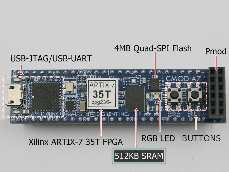
- Digilent Cmod A7
- Papilio DUO
In my case, I chose Digilent Cmod A7-35T (just because I found a good offer in eBay).
Understanding a SRAM datasheetCmod A7 uses the ISSI IS61WV5128BLL-10BLI. It is an asynchronous SRAM, fully documented in ISSI's datasheet [2].
If we take a deep look at the datasheet, we can summarize its main characteristics. See also Figure 3.
- Size: 512 KB.
- 19 address signals.
- 8 bi-directional data signals.
- 3 control signals.
- Access time: 10 ns.
The 3 control signals are: CE, OE and WE. They are all active low.
ce_n(chip enable): disables or enables the chip.we_n(write enable): disables or enables the write operation.oe_n(output enable): disables or enables the output.
If we take a look at Figure 4 we can understand how they have to be asserted.
Note: This SRAM is a little bit simpler than others because its data bus width is only 8 bits. There are others which data bus is 16 bits width. In that case, we will find 2 additional signals: lb_n and ub_n. They are, respectively: lower and upper byte enable.
Another very important part of the datasheet is the one according to the timing parameters. The values of the timing parameters are different for read and write cycles. See Figures 5 and 8.
Read Cycle
As it can be seen on Figure 5, there are 11 timing parameters related to the read cycle. We are going to focus on 6 of them, which are relevant to our design [3]:
- trc: read cycle time, the minimal elapsed time between two read operations. It is about the same as tAA for SRAM.
- tAA: address access time, the time required to obtain stable output data after an address change.
- tOHA: output hold time, the time that the output data remains valid after the address changes. This should not be confused with the hold time of an edge-triggered FF, which is a constraint for the d input.
- tDOE: output enable access time, the time required to obtain valid data after oen is activated.
- tHZOE: output enable to high-Z time, the time for the tri-state buffer to enter the high-impedance state after
oe_nis deactivated. - tLZOE: output enable to low-Z time, the time for the tri-state buffer to leave the high-impedance state after
oe_nis activated. Note that even when the output is no longer in the high-impedance state, the data is still invalid.
The timing diagrams for two types of read operations are shown Figures 6 and 7.
Write Cycle
In case of the write operation, the relevant timing parameters are [3]:
- twc: write cycle time, the minimal elapsed time between two write operations.
- tSA: address setup time, the minimal time that the address must be stable before
we_nis activated. - tHA: address hold time, the minimal time that the address must be stable after
we_nis deactivated. - tPWE1:
we_npulse width, the minimal time thatwe_nmust be asserted. - tso: data setup time, the minimal time that data must be stable before the latching edge (the edge in which
we_nmoves from 0 to 1). - tHD: data hold time, the minimal time that data must be stable after the latching edge.
The timing diagrams for the write operation can be found in [2].
ControllerTo successfully execute a read or write operation, it is important to assert all these signals (address, data and control signals) in a specific order, and make sure they are stable for a certain amount of time.
To achieve that and to interface with the SRAM, we use a memory controller.
Here there are 2 options: you can either write your own controller or use an IP core like Xilinx External Memory Controller (EMC).
Along this article, we will explore the first way.
As previously said, we have an asynchronous SRAM, that means there is no synchronous clock. All reads and writes to this memory occur with asynchronous control signals. Therefore, we need to create a synchronous memory controller that allows us to safely use the memory with our synchronous system. You can think in the controller as a "synchronous wrap" around the SRAM.
Controller using Verilog
In Figure 9, we can see a diagram of how our controller should look like.
The FSM follows the timing diagrams and specifications mentioned above to generate a proper control sequence.
The first thing should be to write a controller as simple as possible to test the functionality. After that, more time can be dedicated to make a more aggressive design.
A very simple and basic SRAM controller could be the following code (Full module code, can be found in the code section):
 assign ce_n = 1'b0;
 assign oe_n = 1'b0;
 assign we_n = rw;
 assign ad = addr;
 assign dio = (rw == 1'b1)? 8'hZZ : data_f2s;
 always @(posedge clk) begin
   if (rw == 1'b1)
     data_s2f_r <= dio;
 end
This design provides large timing margins and does not impose any stringent timing constraints. It has been tested in a Cmod A7 FPGA board, which has 12 MHz clock input, i.e. a period of 83.333 nanoseconds.
As we can see, ce_n (chip enable signal) and oe_n (output enable signal) are activated all the time.
We use a ternary operator for the tri-state buffer. Notice that dio is a bi-directional bus.
Once we already have a controller module, it's time to test it by simulation.
The vendor (ISSI) does not provide an HDL model to test it. Nevertheless, it is not a real problem. We can create it.
This model simulates how we expect the external SRAM to respond.
A very simple model can be the following one (Note the timing checks and delay.
Full code (comented) can be found in my Github):
 specify
   specparam
   Twp = 8,
   Tdw = 6,
   Tdh = 0;
   $width (negedge we_n, Twp);
   $setup (data, posedge we_n, Tdw);
   $hold (posedge we_n, data, Tdh);
 endspecify
 reg [7:0] sram [0:1024];
 always@(posedge we_n)
   if (ce_n == 1'b0)
     sram[addr] <= data;
assign #10 data = (~ce_n & ~oe_n) ? sram[addr] :  8'bz;
Having the controller and the model, we can run a simulation.
Now we have checked that the controller works fine, it is time to build a synthesizable design to test the SRAM.
For the HDL design to test the SRAM, we have to be able to write and read any data in any specific address. Therefore, it is important to have a terminal to select which operation we want to make, and enter any desired data.
For doing that, the design will need the following modules:
- UART: For sending/receiving data to/from FPGA/PC;
- Debouncer: To debounce the reset button;
- FSM: For controlling all the signals and steps in my design;
- SRAM controller.
Once those modules have been written, we will have a circuit like this:
Note: Figure 12 has been created using Xilinx ISE. However, XC7A35T is not supported by ISE. You will have to use Vivado if you want to synthesize this design in Cmod A7's FPGA.
Here is a demonstration on how this design works.
First, we see a menu and I write 8 bits in a random address, and then I read back that same address and check the value written and read from the SRAM is exactly the same.
If this is the first time you work with memories, you will notice something weird. If you power on the FPGA board and then read any random memory address from the SRAM, you'll always find the same data there.
Maybe you were expecting to find rubbish (i.e. different data every time I plug in the board). But that does not happen.
Every SRAM cell has a built in bias that makes it probabilistically tilt towards a particular value at power up.
This value is unique for each SRAM, and there are technologies which use this as a way to create a unique chip identifier to be used for cryptography and other things (Please google “SRAM PUF”).
ConclusionThe controller presented in this article is a very basic and simple controller for educational purposes only. It is not intended to be a controller for any serious design.
In the next article, I will design a much more precise and aggressive controller, and we'll mention clock cycles and exhaustive verification.
It continues in the second article: https://www.hackster.io/salvador-canas/a-practical-introduction-to-sram-memories-using-an-fpga-ii-a18801
You can find the files associated with this project here:
https://github.com/salcanmor/SRAM-tester-for-Cmod-A7-35T/tree/master/basic%20controller
References
[1] Wikipedia. Types of SRAM: https://en.wikipedia.org/wiki/Static_random-access_memory#Types_of_SRAM
[2] Datasheet of ISSI IS61WV5128BLL-10BLI: http://www.issi.com/WW/pdf/61-64WV5128Axx-Bxx.pdf
[3] Chu, Pong P., 1959-. FPGA Prototyping by Verilog Examples Xilinx Spartan -3 Version. Hoboken, N.J. :J. Wiley & Sons, 2008. Print.


Comments