Whitney Knitter
Published © GPL3+

AXI4-Lite Interface Wrapper for Custom RTL in Vivado 2021.2

This project demonstrates how to take a custom RTL module and add an AXI4-Lite interface wrapper to it for use in the Vivado block design.

IntermediateFull instructions provided2 hours6,423
AXI4-Lite Interface Wrapper for Custom RTL in Vivado 2021.2

Things used in this project

Hardware components

Arty Z7-20
Digilent Arty Z7-20
×1
USB-A to Micro-USB Cable
×1
NPN BJT Transistor, 2N3904
×5
Through Hole Resistor, 680 ohm
×8
Through Hole Resistor, 6.8 kohm
×5
Solderless Breadboard Full Size
×1
HP QDSP-6061 Bubble Display (vintage)
×1

Software apps and online services
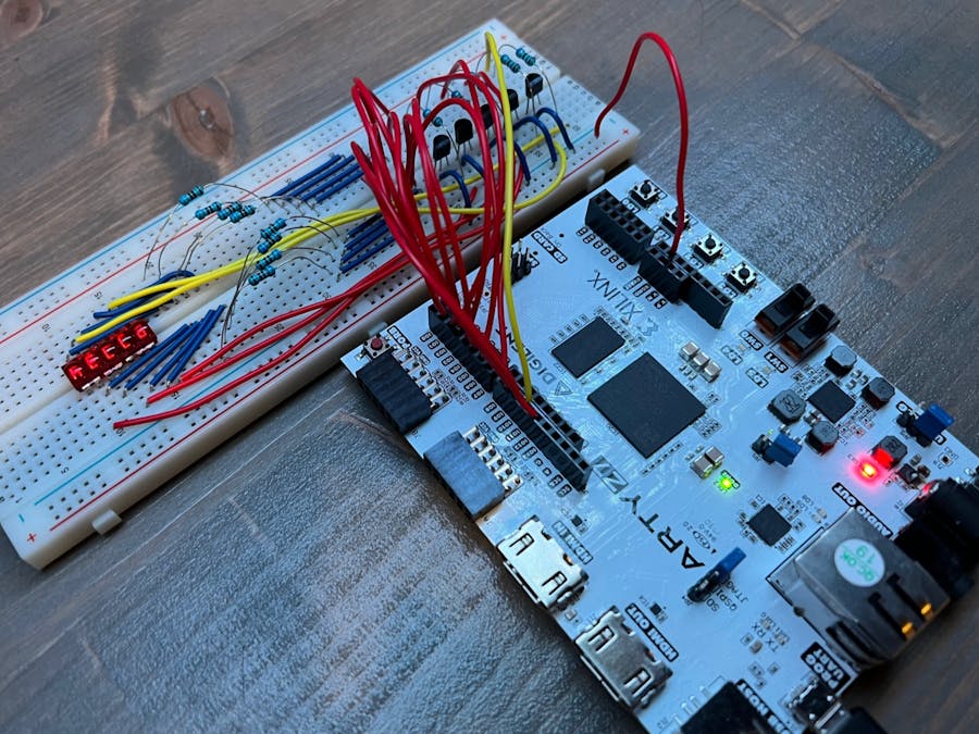
Vivado Design Suite
AMD Vivado Design Suite
Vitis Unified Software Platform
AMD Vitis Unified Software Platform

Story

Read more

Code

axi_qdsp_6061_controller_v1_0.v

Verilog
`timescale 1 ns / 1 ps

	module axi_qdsp_6061_controller_v1_0 #
	(
		// Users to add parameters here

		// User parameters ends
		// Do not modify the parameters beyond this line


		// Parameters of Axi Slave Bus Interface S00_AXI
		parameter integer C_S00_AXI_DATA_WIDTH	= 32,
		parameter integer C_S00_AXI_ADDR_WIDTH	= 4
	)
	(
		// Users to add ports here
		input wire logic_clk,
		input wire reset,
        output reg [7:0] anodeReg,
        output reg [4:0] cathodeReg,
		// User ports ends
		// Do not modify the ports beyond this line


		// Ports of Axi Slave Bus Interface S00_AXI
		input wire  s00_axi_aclk,
		input wire  s00_axi_aresetn,
		input wire [C_S00_AXI_ADDR_WIDTH-1 : 0] s00_axi_awaddr,
		input wire [2 : 0] s00_axi_awprot,
		input wire  s00_axi_awvalid,
		output wire  s00_axi_awready,
		input wire [C_S00_AXI_DATA_WIDTH-1 : 0] s00_axi_wdata,
		input wire [(C_S00_AXI_DATA_WIDTH/8)-1 : 0] s00_axi_wstrb,
		input wire  s00_axi_wvalid,
		output wire  s00_axi_wready,
		output wire [1 : 0] s00_axi_bresp,
		output wire  s00_axi_bvalid,
		input wire  s00_axi_bready,
		input wire [C_S00_AXI_ADDR_WIDTH-1 : 0] s00_axi_araddr,
		input wire [2 : 0] s00_axi_arprot,
		input wire  s00_axi_arvalid,
		output wire  s00_axi_arready,
		output wire [C_S00_AXI_DATA_WIDTH-1 : 0] s00_axi_rdata,
		output wire [1 : 0] s00_axi_rresp,
		output wire  s00_axi_rvalid,
		input wire  s00_axi_rready
	);
// Instantiation of Axi Bus Interface S00_AXI
    wire enable;

	axi_qdsp_6061_controller_v1_0_S00_AXI # ( 
		.C_S_AXI_DATA_WIDTH(C_S00_AXI_DATA_WIDTH),
		.C_S_AXI_ADDR_WIDTH(C_S00_AXI_ADDR_WIDTH)
	) axi_qdsp_6061_controller_v1_0_S00_AXI_inst (
		.logic_enable(enable),
		.S_AXI_ACLK(s00_axi_aclk),
		.S_AXI_ARESETN(s00_axi_aresetn),
		.S_AXI_AWADDR(s00_axi_awaddr),
		.S_AXI_AWPROT(s00_axi_awprot),
		.S_AXI_AWVALID(s00_axi_awvalid),
		.S_AXI_AWREADY(s00_axi_awready),
		.S_AXI_WDATA(s00_axi_wdata),
		.S_AXI_WSTRB(s00_axi_wstrb),
		.S_AXI_WVALID(s00_axi_wvalid),
		.S_AXI_WREADY(s00_axi_wready),
		.S_AXI_BRESP(s00_axi_bresp),
		.S_AXI_BVALID(s00_axi_bvalid),
		.S_AXI_BREADY(s00_axi_bready),
		.S_AXI_ARADDR(s00_axi_araddr),
		.S_AXI_ARPROT(s00_axi_arprot),
		.S_AXI_ARVALID(s00_axi_arvalid),
		.S_AXI_ARREADY(s00_axi_arready),
		.S_AXI_RDATA(s00_axi_rdata),
		.S_AXI_RRESP(s00_axi_rresp),
		.S_AXI_RVALID(s00_axi_rvalid),
		.S_AXI_RREADY(s00_axi_rready)
	);

	// Add user logic here
    parameter zero  = 8'b11111100;
    parameter one   = 8'b01100000;
    parameter two   = 8'b11011010;
    parameter three = 8'b11110010;
    parameter four  = 8'b01100110;
    parameter five  = 8'b10110110;
    parameter six   = 8'b10111110;
    parameter seven = 8'b11100000;
    parameter eight = 8'b11111110;
    parameter nine  = 8'b11110110;     
    parameter k     = 8'b10101110;
    parameter n     = 8'b00101010;
    parameter i     = 8'b00001000;
    parameter t     = 8'b00011110;
    parameter r     = 8'b00001010;
    parameter o     = 8'b00111010;
    parameter c     = 8'b00011010;
    parameter s     = 8'b10110110;
    parameter h     = 8'b00101110;
    parameter e     = 8'b10011110;
    parameter l     = 8'b00011100;
    parameter space = 8'b00000000;
    
    parameter cathodeC1 = 5'b00001;
    parameter cathodeC2 = 5'b00010;
    parameter cathodeC3 = 5'b00100;
    parameter cathodeC4 = 5'b01000;
    parameter cathodeC5 = 5'b10000;
    
    parameter msec_1 = 16'd100000; // 10ns/clk -> 0.001s/0.000000010s = 100000
    
    reg loop_incr_flag;  
    reg [15:0] wait_cnt;
    reg [4:0]  loop_cnt;
    reg [7:0]  incr_flag_cntr;
    reg [7:0]  anodeReg1, anodeReg2, anodeReg3, anodeReg4, anodeReg5;
    
    always @ (posedge logic_clk)
        begin
            if (reset == 1'b0 || enable == 1'b0)
                begin
                    wait_cnt <= 16'd0;	
                    loop_incr_flag <= 1'b0;		
                    cathodeReg <= cathodeC1;
                end
            else
                begin
                    if (wait_cnt < msec_1)
                        begin						
                            loop_incr_flag <= 1'b0;	
                            wait_cnt <= wait_cnt + 1;
                        end
                    else
                        begin					
                            wait_cnt <= 16'd0;
    
                            if (cathodeReg == cathodeC5)
                                begin
                                    loop_incr_flag <= 1'b1;
                                    cathodeReg <= cathodeC1;
                                end
                            else
                                begin
                                    cathodeReg <= cathodeReg << 1;
                                end
                        end
                end
        end 
        
    always @ (posedge logic_clk)
        begin
            if (reset == 1'b0 || enable == 1'b0)
                begin
                    loop_cnt <= 5'd0;
                    incr_flag_cntr <= 8'd0;
                end
            else
                begin
                    if (loop_incr_flag == 1'b1)
                        begin
                            if (incr_flag_cntr == 8'd255)
                                begin
                                    if (loop_cnt == 5'd15)
                                        begin
                                            loop_cnt <= 5'd0;
                                        end
                                    else
                                        begin
                                            loop_cnt <= loop_cnt + 1;
                                        end
                                end
                            else
                                begin
                                    loop_cnt <= loop_cnt;
                                end
                                
                            incr_flag_cntr <= incr_flag_cntr + 1;
                        end
                    else
                        begin
                            loop_cnt <= loop_cnt;
                        end 
                end
        end
    
    always @ (posedge logic_clk)
        begin
            case (cathodeReg)
                cathodeC1 : anodeReg[7:0] <= anodeReg1[7:0];
                cathodeC2 : anodeReg[7:0] <= anodeReg2[7:0];
                cathodeC3 : anodeReg[7:0] <= anodeReg3[7:0];
                cathodeC4 : anodeReg[7:0] <= anodeReg4[7:0];
                cathodeC5 : anodeReg[7:0] <= anodeReg5[7:0];
                default   : anodeReg[7:0] <= anodeReg1[7:0];
            endcase
        end
    
    always @ (posedge logic_clk)
        begin
            case (loop_cnt)
                0 :
                    begin
                        anodeReg1[7:0] <= space;
                        anodeReg2[7:0] <= space;
                        anodeReg3[7:0] <= space;
                        anodeReg4[7:0] <= space;
                        anodeReg5[7:0] <= space;
                    end
                1 :
                    begin
                        anodeReg1[7:0] <= space;
                        anodeReg2[7:0] <= space;
                        anodeReg3[7:0] <= space;
                        anodeReg4[7:0] <= space;
                        anodeReg5[7:0] <= h;
                    end
                2 :
                    begin
                        anodeReg1[7:0] <= space;
                        anodeReg2[7:0] <= space;
                        anodeReg3[7:0] <= space;
                        anodeReg4[7:0] <= h;
                        anodeReg5[7:0] <= e;
                    end
                3 :
                    begin
                        anodeReg1[7:0] <= space;
                        anodeReg2[7:0] <= space;
                        anodeReg3[7:0] <= h;
                        anodeReg4[7:0] <= e;
                        anodeReg5[7:0] <= l;
                    end
                4 :
                    begin
                        anodeReg1[7:0] <= space;
                        anodeReg2[7:0] <= h;
                        anodeReg3[7:0] <= e;
                        anodeReg4[7:0] <= l;
                        anodeReg5[7:0] <= l;
                    end
                5 :
                    begin
                        anodeReg1[7:0] <= h;
                        anodeReg2[7:0] <= e;
                        anodeReg3[7:0] <= l;
                        anodeReg4[7:0] <= l;
                        anodeReg5[7:0] <= o;
                    end
                6 :
                    begin
                        anodeReg1[7:0] <= e;
                        anodeReg2[7:0] <= l;
                        anodeReg3[7:0] <= l;
                        anodeReg4[7:0] <= o;
                        anodeReg5[7:0] <= space;
                    end
                7 :
                    begin
                        anodeReg1[7:0] <= l;
                        anodeReg2[7:0] <= l;
                        anodeReg3[7:0] <= o;
                        anodeReg4[7:0] <= space;
                        anodeReg5[7:0] <= two;
                    end
                8 :
                    begin
                        anodeReg1[7:0] <= l;
                        anodeReg2[7:0] <= o;
                        anodeReg3[7:0] <= space;
                        anodeReg4[7:0] <= two;
                        anodeReg5[7:0] <= zero;
                    end
                9 :
                    begin
                        anodeReg1[7:0] <= o;
                        anodeReg2[7:0] <= space;
                        anodeReg3[7:0] <= two;
                        anodeReg4[7:0] <= zero;
                        anodeReg5[7:0] <= two;
                    end
                10 :
                    begin
                        anodeReg1[7:0] <= space;
                        anodeReg2[7:0] <= two;
                        anodeReg3[7:0] <= zero;
                        anodeReg4[7:0] <= two;
                        anodeReg5[7:0] <= two;
                    end
                11 :
                    begin
                        anodeReg1[7:0] <= two;
                        anodeReg2[7:0] <= zero;
                        anodeReg3[7:0] <= two;
                        anodeReg4[7:0] <= two;
                        anodeReg5[7:0] <= space;
                    end
                12 :
                    begin
                        anodeReg1[7:0] <= zero;
                        anodeReg2[7:0] <= two;
                        anodeReg3[7:0] <= two;
                        anodeReg4[7:0] <= space;
                        anodeReg5[7:0] <= space;
                    end
                13 :
                    begin
                        anodeReg1[7:0] <= two;
                        anodeReg2[7:0] <= two;
                        anodeReg3[7:0] <= space;
                        anodeReg4[7:0] <= space;
                        anodeReg5[7:0] <= space;
                    end
                14 :
                    begin
                        anodeReg1[7:0] <= two;
                        anodeReg2[7:0] <= space;
                        anodeReg3[7:0] <= space;
                        anodeReg4[7:0] <= space;
                        anodeReg5[7:0] <= space;
                    end
                15 :
                    begin
                        anodeReg1[7:0] <= space;
                        anodeReg2[7:0] <= space;
                        anodeReg3[7:0] <= space;
                        anodeReg4[7:0] <= space;
                        anodeReg5[7:0] <= space;
                    end
                default :
                    begin
                        anodeReg1[7:0] <= h;
                        anodeReg2[7:0] <= e;
                        anodeReg3[7:0] <= l;
                        anodeReg4[7:0] <= l;
                        anodeReg5[7:0] <= o;
                    end
            endcase
        end

	// User logic ends 

	endmodule

axi_qdsp_6061_controller_v1_0_S00_AXI.v

Verilog
`timescale 1 ns / 1 ps

	module axi_qdsp_6061_controller_v1_0_S00_AXI #
	(
		// Users to add parameters here

		// User parameters ends
		// Do not modify the parameters beyond this line

		// Width of S_AXI data bus
		parameter integer C_S_AXI_DATA_WIDTH	= 32,
		// Width of S_AXI address bus
		parameter integer C_S_AXI_ADDR_WIDTH	= 4
	)
	(
		// Users to add ports here
		output reg logic_enable,

		// User ports ends
		// Do not modify the ports beyond this line

		// Global Clock Signal
		input wire  S_AXI_ACLK,
		// Global Reset Signal. This Signal is Active LOW
		input wire  S_AXI_ARESETN,
		// Write address (issued by master, acceped by Slave)
		input wire [C_S_AXI_ADDR_WIDTH-1 : 0] S_AXI_AWADDR,
		// Write channel Protection type. This signal indicates the
    		// privilege and security level of the transaction, and whether
    		// the transaction is a data access or an instruction access.
		input wire [2 : 0] S_AXI_AWPROT,
		// Write address valid. This signal indicates that the master signaling
    		// valid write address and control information.
		input wire  S_AXI_AWVALID,
		// Write address ready. This signal indicates that the slave is ready
    		// to accept an address and associated control signals.
		output wire  S_AXI_AWREADY,
		// Write data (issued by master, acceped by Slave) 
		input wire [C_S_AXI_DATA_WIDTH-1 : 0] S_AXI_WDATA,
		// Write strobes. This signal indicates which byte lanes hold
    		// valid data. There is one write strobe bit for each eight
    		// bits of the write data bus.    
		input wire [(C_S_AXI_DATA_WIDTH/8)-1 : 0] S_AXI_WSTRB,
		// Write valid. This signal indicates that valid write
    		// data and strobes are available.
		input wire  S_AXI_WVALID,
		// Write ready. This signal indicates that the slave
    		// can accept the write data.
		output wire  S_AXI_WREADY,
		// Write response. This signal indicates the status
    		// of the write transaction.
		output wire [1 : 0] S_AXI_BRESP,
		// Write response valid. This signal indicates that the channel
    		// is signaling a valid write response.
		output wire  S_AXI_BVALID,
		// Response ready. This signal indicates that the master
    		// can accept a write response.
		input wire  S_AXI_BREADY,
		// Read address (issued by master, acceped by Slave)
		input wire [C_S_AXI_ADDR_WIDTH-1 : 0] S_AXI_ARADDR,
		// Protection type. This signal indicates the privilege
    		// and security level of the transaction, and whether the
    		// transaction is a data access or an instruction access.
		input wire [2 : 0] S_AXI_ARPROT,
		// Read address valid. This signal indicates that the channel
    		// is signaling valid read address and control information.
		input wire  S_AXI_ARVALID,
		// Read address ready. This signal indicates that the slave is
    		// ready to accept an address and associated control signals.
		output wire  S_AXI_ARREADY,
		// Read data (issued by slave)
		output wire [C_S_AXI_DATA_WIDTH-1 : 0] S_AXI_RDATA,
		// Read response. This signal indicates the status of the
    		// read transfer.
		output wire [1 : 0] S_AXI_RRESP,
		// Read valid. This signal indicates that the channel is
    		// signaling the required read data.
		output wire  S_AXI_RVALID,
		// Read ready. This signal indicates that the master can
    		// accept the read data and response information.
		input wire  S_AXI_RREADY
	);

	// AXI4LITE signals
	reg [C_S_AXI_ADDR_WIDTH-1 : 0] 	axi_awaddr;
	reg  	axi_awready;
	reg  	axi_wready;
	reg [1 : 0] 	axi_bresp;
	reg  	axi_bvalid;
	reg [C_S_AXI_ADDR_WIDTH-1 : 0] 	axi_araddr;
	reg  	axi_arready;
	reg [C_S_AXI_DATA_WIDTH-1 : 0] 	axi_rdata;
	reg [1 : 0] 	axi_rresp;
	reg  	axi_rvalid;

	// Example-specific design signals
	// local parameter for addressing 32 bit / 64 bit C_S_AXI_DATA_WIDTH
	// ADDR_LSB is used for addressing 32/64 bit registers/memories
	// ADDR_LSB = 2 for 32 bits (n downto 2)
	// ADDR_LSB = 3 for 64 bits (n downto 3)
	localparam integer ADDR_LSB = (C_S_AXI_DATA_WIDTH/32) + 1;
	localparam integer OPT_MEM_ADDR_BITS = 1;
	//----------------------------------------------
	//-- Signals for user logic register space example
	//------------------------------------------------
	//-- Number of Slave Registers 4
	reg [C_S_AXI_DATA_WIDTH-1:0]	slv_reg0;
	reg [C_S_AXI_DATA_WIDTH-1:0]	slv_reg1;
	reg [C_S_AXI_DATA_WIDTH-1:0]	slv_reg2;
	reg [C_S_AXI_DATA_WIDTH-1:0]	slv_reg3;
	wire	 slv_reg_rden;
	wire	 slv_reg_wren;
	reg [C_S_AXI_DATA_WIDTH-1:0]	 reg_data_out;
	integer	 byte_index;
	reg	 aw_en;

	// I/O Connections assignments

	assign S_AXI_AWREADY	= axi_awready;
	assign S_AXI_WREADY	= axi_wready;
	assign S_AXI_BRESP	= axi_bresp;
	assign S_AXI_BVALID	= axi_bvalid;
	assign S_AXI_ARREADY	= axi_arready;
	assign S_AXI_RDATA	= axi_rdata;
	assign S_AXI_RRESP	= axi_rresp;
	assign S_AXI_RVALID	= axi_rvalid;
	// Implement axi_awready generation
	// axi_awready is asserted for one S_AXI_ACLK clock cycle when both
	// S_AXI_AWVALID and S_AXI_WVALID are asserted. axi_awready is
	// de-asserted when reset is low.

	always @( posedge S_AXI_ACLK )
	begin
	  if ( S_AXI_ARESETN == 1'b0 )
	    begin
	      axi_awready <= 1'b0;
	      aw_en <= 1'b1;
	    end 
	  else
	    begin    
	      if (~axi_awready && S_AXI_AWVALID && S_AXI_WVALID && aw_en)
	        begin
	          // slave is ready to accept write address when 
	          // there is a valid write address and write data
	          // on the write address and data bus. This design 
	          // expects no outstanding transactions. 
	          axi_awready <= 1'b1;
	          aw_en <= 1'b0;
	        end
	        else if (S_AXI_BREADY && axi_bvalid)
	            begin
	              aw_en <= 1'b1;
	              axi_awready <= 1'b0;
	            end
	      else           
	        begin
	          axi_awready <= 1'b0;
	        end
	    end 
	end       

	// Implement axi_awaddr latching
	// This process is used to latch the address when both 
	// S_AXI_AWVALID and S_AXI_WVALID are valid. 

	always @( posedge S_AXI_ACLK )
	begin
	  if ( S_AXI_ARESETN == 1'b0 )
	    begin
	      axi_awaddr <= 0;
	    end 
	  else
	    begin    
	      if (~axi_awready && S_AXI_AWVALID && S_AXI_WVALID && aw_en)
	        begin
	          // Write Address latching 
	          axi_awaddr <= S_AXI_AWADDR;
	        end
	    end 
	end       

	// Implement axi_wready generation
	// axi_wready is asserted for one S_AXI_ACLK clock cycle when both
	// S_AXI_AWVALID and S_AXI_WVALID are asserted. axi_wready is 
	// de-asserted when reset is low. 

	always @( posedge S_AXI_ACLK )
	begin
	  if ( S_AXI_ARESETN == 1'b0 )
	    begin
	      axi_wready <= 1'b0;
	    end 
	  else
	    begin    
	      if (~axi_wready && S_AXI_WVALID && S_AXI_AWVALID && aw_en )
	        begin
	          // slave is ready to accept write data when 
	          // there is a valid write address and write data
	          // on the write address and data bus. This design 
	          // expects no outstanding transactions. 
	          axi_wready <= 1'b1;
	        end
	      else
	        begin
	          axi_wready <= 1'b0;
	        end
	    end 
	end       

	// Implement memory mapped register select and write logic generation
	// The write data is accepted and written to memory mapped registers when
	// axi_awready, S_AXI_WVALID, axi_wready and S_AXI_WVALID are asserted. Write strobes are used to
	// select byte enables of slave registers while writing.
	// These registers are cleared when reset (active low) is applied.
	// Slave register write enable is asserted when valid address and data are available
	// and the slave is ready to accept the write address and write data.
	assign slv_reg_wren = axi_wready && S_AXI_WVALID && axi_awready && S_AXI_AWVALID;

	always @( posedge S_AXI_ACLK )
	begin
	  if ( S_AXI_ARESETN == 1'b0 )
	    begin
	      slv_reg0 <= 0;
	      slv_reg1 <= 0;
	      slv_reg2 <= 0;
	      slv_reg3 <= 0;
	    end 
	  else begin
	    if (slv_reg_wren)
	      begin
	        case ( axi_awaddr[ADDR_LSB+OPT_MEM_ADDR_BITS:ADDR_LSB] )
	          2'h0:
	            for ( byte_index = 0; byte_index <= (C_S_AXI_DATA_WIDTH/8)-1; byte_index = byte_index+1 )
	              if ( S_AXI_WSTRB[byte_index] == 1 ) begin
	                // Respective byte enables are asserted as per write strobes 
	                // Slave register 0
	                slv_reg0[(byte_index*8) +: 8] <= S_AXI_WDATA[(byte_index*8) +: 8];
	              end  
	          2'h1:
	            for ( byte_index = 0; byte_index <= (C_S_AXI_DATA_WIDTH/8)-1; byte_index = byte_index+1 )
	              if ( S_AXI_WSTRB[byte_index] == 1 ) begin
	                // Respective byte enables are asserted as per write strobes 
	                // Slave register 1
	                slv_reg1[(byte_index*8) +: 8] <= S_AXI_WDATA[(byte_index*8) +: 8];
	              end  
	          2'h2:
	            for ( byte_index = 0; byte_index <= (C_S_AXI_DATA_WIDTH/8)-1; byte_index = byte_index+1 )
	              if ( S_AXI_WSTRB[byte_index] == 1 ) begin
	                // Respective byte enables are asserted as per write strobes 
	                // Slave register 2
	                slv_reg2[(byte_index*8) +: 8] <= S_AXI_WDATA[(byte_index*8) +: 8];
	              end  
	          2'h3:
	            for ( byte_index = 0; byte_index <= (C_S_AXI_DATA_WIDTH/8)-1; byte_index = byte_index+1 )
	              if ( S_AXI_WSTRB[byte_index] == 1 ) begin
	                // Respective byte enables are asserted as per write strobes 
	                // Slave register 3
	                slv_reg3[(byte_index*8) +: 8] <= S_AXI_WDATA[(byte_index*8) +: 8];
	              end  
	          default : begin
	                      slv_reg0 <= slv_reg0;
	                      slv_reg1 <= slv_reg1;
	                      slv_reg2 <= slv_reg2;
	                      slv_reg3 <= slv_reg3;
	                    end
	        endcase
	      end
	  end
	end    

	// Implement write response logic generation
	// The write response and response valid signals are asserted by the slave 
	// when axi_wready, S_AXI_WVALID, axi_wready and S_AXI_WVALID are asserted.  
	// This marks the acceptance of address and indicates the status of 
	// write transaction.

	always @( posedge S_AXI_ACLK )
	begin
	  if ( S_AXI_ARESETN == 1'b0 )
	    begin
	      axi_bvalid  <= 0;
	      axi_bresp   <= 2'b0;
	    end 
	  else
	    begin    
	      if (axi_awready && S_AXI_AWVALID && ~axi_bvalid && axi_wready && S_AXI_WVALID)
	        begin
	          // indicates a valid write response is available
	          axi_bvalid <= 1'b1;
	          axi_bresp  <= 2'b0; // 'OKAY' response 
	        end                   // work error responses in future
	      else
	        begin
	          if (S_AXI_BREADY && axi_bvalid) 
	            //check if bready is asserted while bvalid is high) 
	            //(there is a possibility that bready is always asserted high)   
	            begin
	              axi_bvalid <= 1'b0; 
	            end  
	        end
	    end
	end   

	// Implement axi_arready generation
	// axi_arready is asserted for one S_AXI_ACLK clock cycle when
	// S_AXI_ARVALID is asserted. axi_awready is 
	// de-asserted when reset (active low) is asserted. 
	// The read address is also latched when S_AXI_ARVALID is 
	// asserted. axi_araddr is reset to zero on reset assertion.

	always @( posedge S_AXI_ACLK )
	begin
	  if ( S_AXI_ARESETN == 1'b0 )
	    begin
	      axi_arready <= 1'b0;
	      axi_araddr  <= 32'b0;
	    end 
	  else
	    begin    
	      if (~axi_arready && S_AXI_ARVALID)
	        begin
	          // indicates that the slave has acceped the valid read address
	          axi_arready <= 1'b1;
	          // Read address latching
	          axi_araddr  <= S_AXI_ARADDR;
	        end
	      else
	        begin
	          axi_arready <= 1'b0;
	        end
	    end 
	end       

	// Implement axi_arvalid generation
	// axi_rvalid is asserted for one S_AXI_ACLK clock cycle when both 
	// S_AXI_ARVALID and axi_arready are asserted. The slave registers 
	// data are available on the axi_rdata bus at this instance. The 
	// assertion of axi_rvalid marks the validity of read data on the 
	// bus and axi_rresp indicates the status of read transaction.axi_rvalid 
	// is deasserted on reset (active low). axi_rresp and axi_rdata are 
	// cleared to zero on reset (active low).  
	always @( posedge S_AXI_ACLK )
	begin
	  if ( S_AXI_ARESETN == 1'b0 )
	    begin
	      axi_rvalid <= 0;
	      axi_rresp  <= 0;
	    end 
	  else
	    begin    
	      if (axi_arready && S_AXI_ARVALID && ~axi_rvalid)
	        begin
	          // Valid read data is available at the read data bus
	          axi_rvalid <= 1'b1;
	          axi_rresp  <= 2'b0; // 'OKAY' response
	        end   
	      else if (axi_rvalid && S_AXI_RREADY)
	        begin
	          // Read data is accepted by the master
	          axi_rvalid <= 1'b0;
	        end                
	    end
	end    

	// Implement memory mapped register select and read logic generation
	// Slave register read enable is asserted when valid address is available
	// and the slave is ready to accept the read address.
	assign slv_reg_rden = axi_arready & S_AXI_ARVALID & ~axi_rvalid;
	always @(*)
	begin
	      // Address decoding for reading registers
	      case ( axi_araddr[ADDR_LSB+OPT_MEM_ADDR_BITS:ADDR_LSB] )
	        2'h0   : reg_data_out <= slv_reg0;
	        2'h1   : reg_data_out <= slv_reg1;
	        2'h2   : reg_data_out <= slv_reg2;
	        2'h3   : reg_data_out <= slv_reg3;
	        default : reg_data_out <= 0;
	      endcase
	end

	// Output register or memory read data
	always @( posedge S_AXI_ACLK )
	begin
	  if ( S_AXI_ARESETN == 1'b0 )
	    begin
	      axi_rdata  <= 0;
	    end 
	  else
	    begin    
	      // When there is a valid read address (S_AXI_ARVALID) with 
	      // acceptance of read address by the slave (axi_arready), 
	      // output the read dada 
	      if (slv_reg_rden)
	        begin
	          axi_rdata <= reg_data_out;     // register read data
	        end   
	    end
	end    

	// Add user logic here
    always @ (posedge S_AXI_ACLK)
	   begin
	       if (S_AXI_ARESETN == 1'b0)
	           begin
	               logic_enable <= 1'b0;
	           end
	       else
	           begin
	               if (slv_reg0 == 32'hffffffff)
	                   begin
	                       logic_enable <= 1'b1;
	                   end
	               else
	                   begin
	                       logic_enable <= logic_enable;
	                   end
	           end
        end   

	// User logic ends  

	endmodule 

axi_qdsp_6061_controller.c

C/C++
/***************************** Include Files *******************************/
#include "axi_qdsp_6061_controller.h"
#include "xparameters.h"
#include "stdio.h"
#include "xil_io.h"

#define slave_reg0    AXI_QDSP_6061_CONTROLLER_S00_AXI_SLV_REG0_OFFSET
#define slave_reg1    AXI_QDSP_6061_CONTROLLER_S00_AXI_SLV_REG1_OFFSET
#define slave_reg2    AXI_QDSP_6061_CONTROLLER_S00_AXI_SLV_REG2_OFFSET
#define slave_reg3    AXI_QDSP_6061_CONTROLLER_S00_AXI_SLV_REG3_OFFSET
/************************** Function Definitions ***************************/
XStatus QDSP6061_WriteReg(int baseaddr_p, u32 write_data){

	u32 baseaddr = (u32)baseaddr_p;

	AXI_QDSP_6061_CONTROLLER_mWriteReg (baseaddr, slave_reg0, write_data);

	return XST_SUCCESS;

}

u32 QDSP6061_ReadReg(int baseaddr_p){

	u32 data[4];
	int read_loop_index;

	u32 baseaddr = (u32)baseaddr_p;

	for (read_loop_index = 0 ; read_loop_index < 4; read_loop_index++){
		data[read_loop_index] = AXI_QDSP_6061_CONTROLLER_mReadReg (baseaddr, read_loop_index*4);
	}

	return *data;

}

axi_qdsp_6061_controller.h

C Header File
#ifndef AXI_QDSP_6061_CONTROLLER_H
#define AXI_QDSP_6061_CONTROLLER_H


/****************** Include Files ********************/
#include "xil_types.h"
#include "xstatus.h"

#define AXI_QDSP_6061_CONTROLLER_S00_AXI_SLV_REG0_OFFSET 0
#define AXI_QDSP_6061_CONTROLLER_S00_AXI_SLV_REG1_OFFSET 4
#define AXI_QDSP_6061_CONTROLLER_S00_AXI_SLV_REG2_OFFSET 8
#define AXI_QDSP_6061_CONTROLLER_S00_AXI_SLV_REG3_OFFSET 12


/**************************** Type Definitions *****************************/
/**
 *
 * Write a value to a AXI_QDSP_6061_CONTROLLER register. A 32 bit write is performed.
 * If the component is implemented in a smaller width, only the least
 * significant data is written.
 *
 * @param   BaseAddress is the base address of the AXI_QDSP_6061_CONTROLLERdevice.
 * @param   RegOffset is the register offset from the base to write to.
 * @param   Data is the data written to the register.
 *
 * @return  None.
 *
 * @note
 * C-style signature:
 * 	void AXI_QDSP_6061_CONTROLLER_mWriteReg(u32 BaseAddress, unsigned RegOffset, u32 Data)
 *
 */
#define AXI_QDSP_6061_CONTROLLER_mWriteReg(BaseAddress, RegOffset, Data) \
  	Xil_Out32((BaseAddress) + (RegOffset), (u32)(Data))

/**
 *
 * Read a value from a AXI_QDSP_6061_CONTROLLER register. A 32 bit read is performed.
 * If the component is implemented in a smaller width, only the least
 * significant data is read from the register. The most significant data
 * will be read as 0.
 *
 * @param   BaseAddress is the base address of the AXI_QDSP_6061_CONTROLLER device.
 * @param   RegOffset is the register offset from the base to write to.
 *
 * @return  Data is the data from the register.
 *
 * @note
 * C-style signature:
 * 	u32 AXI_QDSP_6061_CONTROLLER_mReadReg(u32 BaseAddress, unsigned RegOffset)
 *
 */
#define AXI_QDSP_6061_CONTROLLER_mReadReg(BaseAddress, RegOffset) \
    Xil_In32((BaseAddress) + (RegOffset))

/************************** Function Prototypes ****************************/
/**
 *
 * Run a self-test on the driver/device. Note this may be a destructive test if
 * resets of the device are performed.
 *
 * If the hardware system is not built correctly, this function may never
 * return to the caller.
 *
 * @param   baseaddr_p is the base address of the AXI_QDSP_6061_CONTROLLER instance to be worked on.
 *
 * @return
 *
 *    - XST_SUCCESS   if all self-test code passed
 *    - XST_FAILURE   if any self-test code failed
 *
 * @note    Caching must be turned off for this function to work.
 * @note    Self test may fail if data memory and device are not on the same bus.
 *
 */
XStatus AXI_QDSP_6061_CONTROLLER_Reg_SelfTest(int baseaddr_p);

XStatus QDSP6061_WriteReg(int baseaddr_p, u32 write_data);
u32 QDSP6061_ReadReg(int baseaddr_p);

#endif // AXI_QDSP_6061_CONTROLLER_H

main.c

C/C++
/******************************************************************************
*
* Copyright (C) 2009 - 2014 Xilinx, Inc.  All rights reserved.
*
* Permission is hereby granted, free of charge, to any person obtaining a copy
* of this software and associated documentation files (the "Software"), to deal
* in the Software without restriction, including without limitation the rights
* to use, copy, modify, merge, publish, distribute, sublicense, and/or sell
* copies of the Software, and to permit persons to whom the Software is
* furnished to do so, subject to the following conditions:
*
* The above copyright notice and this permission notice shall be included in
* all copies or substantial portions of the Software.
*
* Use of the Software is limited solely to applications:
* (a) running on a Xilinx device, or
* (b) that interact with a Xilinx device through a bus or interconnect.
*
* THE SOFTWARE IS PROVIDED "AS IS", WITHOUT WARRANTY OF ANY KIND, EXPRESS OR
* IMPLIED, INCLUDING BUT NOT LIMITED TO THE WARRANTIES OF MERCHANTABILITY,
* FITNESS FOR A PARTICULAR PURPOSE AND NONINFRINGEMENT. IN NO EVENT SHALL
* XILINX  BE LIABLE FOR ANY CLAIM, DAMAGES OR OTHER LIABILITY,
* WHETHER IN AN ACTION OF CONTRACT, TORT OR OTHERWISE, ARISING FROM, OUT OF
* OR IN CONNECTION WITH THE SOFTWARE OR THE USE OR OTHER DEALINGS IN THE
* SOFTWARE.
*
* Except as contained in this notice, the name of the Xilinx shall not be used
* in advertising or otherwise to promote the sale, use or other dealings in
* this Software without prior written authorization from Xilinx.
*
******************************************************************************/

/*
 * helloworld.c: simple test application
 *
 * This application configures UART 16550 to baud rate 9600.
 * PS7 UART (Zynq) is not initialized by this application, since
 * bootrom/bsp configures it to baud rate 115200
 *
 * ------------------------------------------------
 * | UART TYPE   BAUD RATE                        |
 * ------------------------------------------------
 *   uartns550   9600
 *   uartlite    Configurable only in HW design
 *   ps7_uart    115200 (configured by bootrom/bsp)
 */

#include <stdio.h>
#include <string.h>
#include <stdlib.h>
#include <unistd.h>

#include "stdio.h"
#include "xgpio.h"
#include "xil_io.h"
#include "xstatus.h"
#include "platform.h"
#include "xil_types.h"
#include "xil_printf.h"
#include "xil_assert.h"
#include "xparameters.h"
#include "xil_exception.h"
#include "axi_qdsp_6061_controller.h"

#define LEDs_DeviceID           XPAR_AXI_GPIO_LEDS_DEVICE_ID
#define QDSP6061_DeviceID       XPAR_AXI_QDSP_6061_CONTRO_0_DEVICE_ID
#define QDSP6061_BaseAddr       XPAR_AXI_QDSP_6061_CONTRO_0_S00_AXI_BASEADDR
#define QDSP6061_Enable_Mask    0xffffffff

int status;

int main()
{
    init_platform();

	print("Hello World!\n\r");

    int BaseAddr = QDSP6061_BaseAddr;
	u32 write_data = QDSP6061_Enable_Mask;

	status = QDSP6061_WriteReg(BaseAddr, write_data);

	if(status != XST_SUCCESS)
	{
		xil_printf("Failed to write to registers of QDSP-6061 Interface.\n\r");
		return XST_FAILURE;
	}

    print("Successfully ran Hello World application");
    cleanup_platform();
    return 0;
}

Credits

Whitney Knitter

Whitney Knitter

155 projects • 1552 followers
All thoughts/opinions are my own and do not reflect those of any company/entity I currently/previously associate with.

Comments