

Hardware components | ||||||
 |
| × | 1 | |||
| × | 1 | ||||
 |
| × | 1 | |||
| × | 1 | ||||
| × | 1 | ||||
| × | 1 | ||||
| × | 1 | ||||
| × | 1 | ||||
Software apps and online services | ||||||
| ||||||
| ||||||
Newtonian physics describe the behavior or very large bodies/particles within our universe. With certain assumptions, the laws can be applied to bodies/particles ranging from astronomical size to a golf ball (and even smaller), The interactions between different particle are governed by the following equation of gravity.
In an N-particle system, each particle experiences a force by other (N-1) particle. The result of the combined sum of forces result in acceleration of the said particle. Similarly, all other (N-1) particle experience force from other particles in the system simultaneously. The resulting acceleration of all the particles, combined with initial position in space, initial velocity and time-step derive new position of all the N-particles respectively. For the sake of simplicity in implementation, the following assumptions are made:
1. All particles are point masses
2. G=1
3. Introduce a fudge factor in gravity calculations toavoid errors when two point masses are at exactly same co-ordinates.
The design has been implemented to enable user to load initial co-ordinates, mass, a "softening factor" and simulation time-step in 16b signed integer format through python software. Although floating point add, subtract and multiply is provided by Vivado environment, an effort was put to design these for custom floating point format.
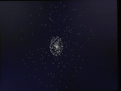
Design: Proof of ConceptThe algorithm was implemented and simulated using python software, The following is the main algorithm and screen capture of the particle simulation performed on PC before the hardware implementation was carried out.
This algorithm has a computational complexity of N**2 due to iterative process. This is a great opportunity for implementing an accelerator in hardware. You can try nbody_x86.py to see how slow the particle simulation is running in just software. The particle simulation will run much faster with accelerators implemented in hardware.
This algorithm can be vectorized, hence reducing the complexity to O(N) if a vector processor is used. The below example is to identify the critical portions of algorithm that are compute intensive and provide accelerator for them in fabric/PL.
Let’s say at time t0, all the particles’ information of position and velocity are known.
Consider 2 particle system. The acceleration on 1st particle due to 2nd particle is calculated as follows:
a =(G * m2)/r**2
To preserve the directional information of acceleration: a = (G * m2*|r|)/r**3
NBody problem:
1. The above concept can be extended to N body system.
2. In GRAPE-6 [x], a softening factor“ε” was used to study detailed effects of size. For this project, is was set to 0.
3. Another softening factor was used to prevent different particles from coming extremely close to each other, i.e. to prevent “r~=0”, as shown by the variable "sf" in above python software.
Hardware DesignThe design incorporates 8 parallel accelerator engines that can completely support up to 4000 bodies!
Implementation with 8 Parallel Accelerators
The original design had 1 accelerator running at 75 MHz. Addition of 7 more accelerators in parallel and more than doubling the operating frequency increased power consumption by about 1 W. Data for 1 accelerator is shown in a later section. Data for 8 parallel accelerators is given in this table here.
Performance
Design meets timing at 200 MHz for 4000 particles! Floating point add and multiply have been modified by adding pipelines.
Implementation with Just 1 Accelerator at 200MHz - Data for Comparison
In spite of the complex logic, The implementation consumes the following resources on XCZU3EG with a single gravity compute engine. One gravity engine can compute interactions between 1024 particles (dictated by the depth of input and output BRAMs). The timing was successfully closed at 200 MHz. Pipelining was implemented in the gravity engine. Reset pipelining was implemented in each local module to optimize global reset propagation routing. Entire design runs on a single clock source.
Floating Point Arithmetic
As the numbers in scientific computations range from small extremes to astronomically large values, IEEE754 FP32 was the initial choice of floating point arithmetic. In IEEE754 FP32, numbers are represented by 1 sign bit, 8 exponent bits and 23 mantissa bits as shown in the figure:
However, DSP48E2 can perform only 27bx18b multiplications. Thus, a choice was made to use a custom floating point representation with only 18 mantissa bits. Thus, the floating point arithmetic in this design uses 27b floating point representation.
Smallest number that can be represented in this format: +/- 1.000000000000000001 x 2**(-126)
Largest number that can be represented in this format: +/- 1.111111111111111111 x 2**(127)
Bias of the exponent is 127
The IEEE 754 conditions of NaN, Overflow, and Underflow have not been implemented to the fullest extent.
Implemented FP Arithmetic
IPI based Floating point arithmetic was implemented. Floating point add, multiply were customized to 27 bits for efficient use of DSP48 while floating point inverse square root was fixed to single precision floating point notation due to customization limits. Int16 to floating point, floating point to int16 was also done using Xilinx IPs.
Flow Diagram
The following figure shows a top level view of RAMs, compute engine, pipelined gravity engine, etc.
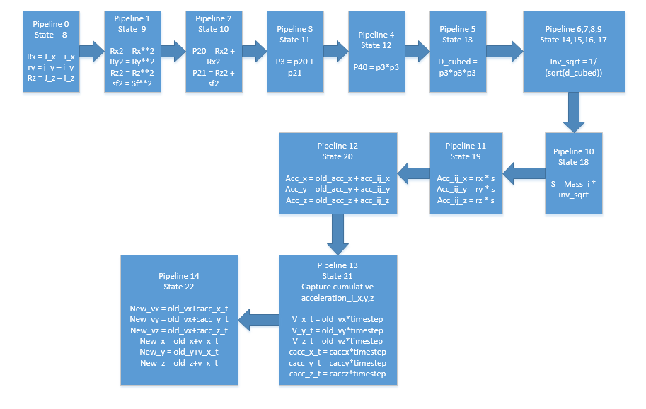
Gravity Engine
The gravity engine is the core of the design. It is implemented as per the algorithm shown in above diagram. The following diagram shows the implementation details of the gravity engine and all the 15 pipelines.
Control and Status Registers; Address Spaces
All BRAMs are controlled using a BRAM controller developed in RTL based on APB3 bus. AXI -APB3 bridge was instantiated in block design. Similarly, an additional APB control and status register bank was implemented in order to control the compute engine. The following are address segments and register spaces:
Design Hierarchy
i_design_1 is the PS system and i_compute_engine is hardware design implemented in the PL part.
Software Flow
Python software was written on PYNQ framework to perform the following actions in sequence:
1. Calculate initial conditions of x, y, z, m of N particles in system, softening factor and simulation time step.
2. Configure the compute engine by loading the int16 x, y, z, m values into BRAMs
3. Start compute engine
4. Wait for compute engine to finish one time step
5. Retrieve the new x, y, z from TXRAMs
6. Create a DisplayPort frame using DisplayPort module. Zero the frame, load the frame with new data and write the frame to monitor.
7. Repeat!
DisplayPort was configured to 1280 x 720 pixels
The new positions of particles can be well beyond monitor size.They are just not shown.
Step 1: Build the FPGA Bitstream from Provided Source FilesThis step may take 45 min to a couple hours, depending on how fast your computer is when running Vivado. The compute time for building is because we are going for high performance with 8 parallel accelerators at 200 MHz.
If you would like to skip this build step, you can use the provided nbodypynq.bit and nbodypynq.tcl from the attachments section.
1. Create a directory on your machine, which we will refer to as <workspace>.
2. Create directory "src" in <workspace>.
3. Download all source files and place them in "src" directory.
4. Open Vivado 2018.3.
5. In the Vivado TCL console
a. cd <workspace>
b. source./src/nbody.tcl
6. Wait for the bitstream to be generated. This may take 45 min to a few hours, depending on your machine. The Vivado project will be in <workspace>/nbody
7. The necessary files to be loaded onto the Ultra96 will be in
<workspace>/nbody/pynq_overlay_files/ and<workspace>/src/nbody.ipynb
Step 2: Set Up the Ultra96 Board1. Download the PYNQ image for Ultra96 from www.pynq.io/board.html
2. Put that PYNQ image on your micro SD card by following the instructions at https://pynq.readthedocs.io/en/latest/appendix.html#writing-the-sd-card and put the micro SD card in the slot on the Ultra96. Make sure it is inserted fully.
3. Plug in your Display Port monitor into the Ultra96 board using the mini Display Port connector. Make sure the monitor is at least 1280 x 720 resolution.
4. (Optional) Plug in a USB mouse and USB keyboard into the USB ports of the Ultra96 board.
5. Follow the USB cable (preferred) or WiFi connection methods in this video for setting up PYNQ on the Ultra96:
6. With the board turned on and connected to your computer, refer to https://ultra96-pynq.readthedocs.io/en/latest/getting_started.html#accessing-files-on-the-board for how to access the files on the Ultra96.
a. If you are connecting the board to your computer via the micro USB cable (USB Ethernet, preferred method), \\PYNQ refers to \\192.168.3.1
b. If you are connecting the board to your computer via WiFi, \\PYNQ refers to \\192.168.2.1
7. Create directories named "nbody-single" and“nbody-parallel” in \\PYNQ\xilinx\pynq\overlays\
8. Copy the files (nbodypynq.bit, nbodyoverlay.tcl) from <workspace>/nbody/pynq_overlay_files/ to \\PYNQ\xilinx\pynq\overlays\nbody-single\ or nbody-parallel, depending on if you have defined PARALLEL in vars.vh. The provided vars.vh is the nbody-parallel configuration.
9. Create a directory named "nbody" in \\PYNQ\xilinx\jupyter_notebooks\
10. Copy Jupyter notebook <workspace>/src/nbody.ipynb to \\PYNQ\xilinx\jupyter_notebooks\nbody\
Step 3: Use the Jupyter Notebook to Run the Particle SimulationA PYNQ Desktop should be displayed on the Display Port monitor attached to the Ultra96, with a “Welcome to PYNQ” getting started page open in the Chromium browser. You have the option to interact with the Ultra96 board using the mouse and keyboard (if you plugged those into the Ultra96) in the Chromium browser to use the Jupyter notebooks. You may find it easier to use the Jupyter notebooks from your computer that is connected to the Ultra96 over the microUSB cable.
1. In a web browser, navigate to the nbody Jupyter notebook by going to the IP address for connecting to the board (e.g.192.168.3.1). When connecting from another computer, you may be asked for a password. It’s “xilinx", all lowercase with no quotation marks.
For more information on connecting to the Pynq Jupyter notebooks please refer to https://ultra96-pynq.readthedocs.io/en/latest/getting_started.html#connecting-to-jupyter-notebooks
2. Update the line:
overlay =Overlay("…")
to point to the desired overlay (e.g. /home/xilinx/pynq/overlays/nbody-parallel/nbodypynq.bit if vars.vh had PARALLEL defined)
3. Click on the step with all the code and click the Run button to run it.
Wait a about 10 seconds. Then, you will see the monitor go dark for about 5 seconds and the particle simulation will run for about 45 seconds. (During this time, the mouse & keyboard attached to the Ultra96 will not work) All bodies with mass < average of all masses are colored in white and others in red.(You can ignore the HWH file warning that appears in the Jupyter notebook window)
4. Try setting initial_condition to 1, 2, and 3 and running again in the Jupyter notebook to see different particle simulations displayed
5. When you are done, be sure to shut down theUltra96 properly, to avoid corrupting the root file system. One way to do this is to open a terminal fromthe browser in the Jupyter Notebooks area, or refer to https://ultra96-pynq.readthedocs.io/en/latest/getting_started.html#opening-a-usb-serial-terminal
Enter the command “shutdown -h now” and let theboard do a clean shutdown.
Modifications to Hardware Design That You Can Try
A. If `define PARALLEL is commented out in <workspace>/src/vars.vh, a single compute engine is implemented. Otherwise, 8 parallel compute engines are implemented in hardware, utilizing more PL resources. You could compare parallel vs. single implementations.
B. Max. number of particles could be changed in <workspace>/src/vars.vh. However, the device meets timing with max. particles of up to 4000, at 200 MHz clock frequency. If more particles are required, the clock frequency must be reduced and timing closure becomes difficult as utilization skyrockets. You would need to widen the address bus to increase the number of particles to 8000 or 16000
C. If execute units number is changed, final stages of the pipelines in parallel_gravity_accelerator needs to be manually modified.
Verilog Simulation for Hardware Development
1. Two testbenches are provided
(a) testbench.v
(b) testbench_fp_arithmetic.v
2. These can be added to the Vivado project and to do circuit simulation of any hardware design modifications you make
3. To save time, modify nbody.tcl to build the project only and not generate bitstream.
- nbody_x86.py Python implementation of N-body particle simulation
- nbodypynq.bit Pre-built bitstream for Pynq overlay
- nbodypynq.tcl Pre-built TCL script for Pynq overlay
- apb3_bram_cntrl.v
- apb3_regbank.v
- compute_engine.v
- design_1.tcl
- Apache 2.0 license
- design_fixed_to_float.tcl
- design_float_to_fixed.tcl
- design_fp_add.tcl
- design_fp_invsqrt.tcl
- design_fp_mult.tcl
- gravity_accelerator.v
- nbody.ipynb Jupyter Notebook
- nbody.tcl
- nbody.xdc
- parallel_gravity_accelerator.v
- reset_pipe.v
- testbench.v
- testbench_fp_arithmetic.v
- top.v
- vars.vh
- xilinx_simple_dual_port_1_clock_ram.v
- xlnx_tdpram_macro.v
- design_1_wrapper.v
nbody_x86.py Python implementation of N-body particle simulation
Python##########################################################################
# Copyright 2019 Xilinx
#
# Licensed under the Apache License, Version 2.0 (the "License");
# you may not use this file except in compliance with the License.
# You may obtain a copy of the License at
#
# http://www.apache.org/licenses/LICENSE-2.0
#
# Unless required by applicable law or agreed to in writing, software
# distributed under the License is distributed on an "AS IS" BASIS,
# WITHOUT WARRANTIES OR CONDITIONS OF ANY KIND, either express or implied.
# See the License for the specific language governing permissions and
# limitations under the License.
#
##########################################################################
#
# 4/4/2019 - Rajeev Patwari
#
# N-Body simulations
# Software to simulate N-body interactions based on Newtonian Gravity
# calculations. The system is confined to point mass bodies with some
# limitations
# This simulation is inspiration to design FPGA accelerator
# Testcase#1 shows why FPGA parallel acceleration is required!
#
# References:
# 1. http://cc.doc.ic.ac.uk/projects/prj_axel/nbody.html
#
# SW installations: Anaconda with Python 3.7 from here
# https://www.anaconda.com/distribution/
#
##########################################################################
import numpy as np
import matplotlib.pyplot as plt
import matplotlib.animation as animation
import mpl_toolkits.mplot3d.axes3d as p3
import random
import math
# ----------- configure before run - begin
# select a test case between 1 and 10
# uncomment one of the following
#testcase = 1 # n=500; very slow on pc - this is why we need accelerator!
testcase = 2 # n=2
#testcase = 3 # n=12
#testcase = 4 # n=3
#testcase = 5 # n=500; very slow on PC
#testcase = 6 # n=500; very slow on PC
#testcase = 7 # n=500; very slow on PC
# ----------- configure before run - end
# Fixing random state for reproducibility
random.seed(19680801)
# initialize particle positions, mass and initial velocity
graphlim = 4000
numparticles = 500
timestep = np.float(100)
if testcase==1:
x = list(np.random.uniform(-3000,3000,numparticles))
y = list(np.random.uniform(-3000,3000,numparticles))
z = list(np.random.uniform(-3000,3000,numparticles))
mass = list(np.random.uniform(100,110,numparticles))
vx = list(np.random.uniform(0,0,numparticles ))
vy = list(np.random.uniform(0,0,numparticles ))
vz = list(np.random.uniform(0,0,numparticles ))
mass[0] = 100
sf = 4000.0
elif testcase==2:
x = [300, -300]
y = [0,0]
z = [0,0]
mass = [295, 300]
vx = [-0.1,0]
vy = [0.1,0]
vz = [0,0]
sf = 600.0
numparticles = 2
elif testcase==3:
numparticles = 12
x = [100, 100, -100,-100, 100, 100, -100,-100, 100, 100, -100,-100]
y = [100, -100, 100, -100,100, -100, 100, -100, 100, -100, 100, -100]
z = [0, 0, 0, 0, 100, 100, 100, 100, -100,-100, -100, -100]
mass = [0.5 for i in range(0,numparticles,1)]
vx = [0.0 for i in range(0,numparticles,1)]
vy = [0.0 for i in range(0,numparticles,1)]
vz = [0.0 for i in range(0,numparticles,1)]
sf = 200.0
elif testcase==4: # 2 planets trying to orbit a star
numparticles = 3
x = [0, 0, 10]
y = [0, 25, 10]
z = [0, 0, 0 ]
mass = [10, 10, 5]
vx = [0.0, 0.0, 0.0]
vy = [0.0, 0.0, 0.0 ]
vz = [0.0, 0.0, 0.0]
sf = 2
graphlim = 800
timestep = np.float(1)
elif testcase==5:
lim = 3000.0/2
x = list(lim*np.random.random_sample((numparticles,)))
y = list(lim*np.random.random_sample((numparticles,)))
z = list(lim*np.random.random_sample((numparticles,)))
mass = list(3000*np.random.random_sample((numparticles,)))
vx = list(np.random.uniform(-1,1,numparticles ))
vy = list(np.random.uniform(-1,1,numparticles ))
vz = list(np.random.uniform(-1,1,numparticles ))
mass[0] = 100
sf = 4000.0
graphlim = 8000
elif testcase==6:
radius, h_max, v_max = 1000, 1280, 720
theta = np.linspace(0, 2*np.pi, numparticles)
a, b = 1 * np.cos(theta), 1 * np.sin(theta)
r = np.random.rand((numparticles))
x, y = radius*r * np.cos(theta), radius*r * np.sin(theta)
x = [int(i+640) for i in x]
y = [int(i+360) for i in y]
mass = [random.randint(10, 110) for i in range(0, numparticles)]
z = [0 for i in range(0, numparticles)]
#x[0], y[0], mass[0] = 640, 360, 10000
vx = [0 for i in range(0, numparticles)]
vy = [0 for i in range(0, numparticles)]
vz = [0 for i in range(0, numparticles)]
sf = 300.0
timestep = np.float(5)
graphlim = 1500
else:
print ("Chose between 1 to 6 and re-run")
# Create new Figure with black background
fig = plt.figure()
ax = p3.Axes3D(fig)
# Add a subplot with no frame, set limits
ax.set_xlim3d(-graphlim, graphlim)
ax.set_ylim3d(-graphlim, graphlim)
ax.set_zlim3d(-graphlim, graphlim)
ax.set_xlabel('X Label')
ax.set_ylabel('Y Label')
ax.set_zlabel('Z Label')
print(len(x), len(y), len(z), len(vx), len(vy), len(vz), len(mass))
def update(*args):
""" can be parameerized if needed """
global x,y,vx,vy,mass,numparticles, sf
accx = [0.0 for i in range(0, numparticles)]
accy = [0.0 for i in range(0, numparticles)]
accz = [0.0 for i in range(0, numparticles)]
for i in range(0, numparticles, 1):
for j in range(0, numparticles, 1):
if (j!=i):
rx = x[j] - x[i]
ry = y[j] - y[i]
rz = z[j] - z[i]
dd = np.power(rx,2) + np.power(ry,2) + np.power(rz,2) + sf*sf
#print(np.power(dd,3))
d = 1/np.sqrt(np.power(dd,3))
s = mass[j]*d
accx[i] += rx*s
accy[i] += ry*s
accz[i] += rz*s
#print(accx[0], x[0])
x[i] += vx[i]*timestep
y[i] += vy[i]*timestep
z[i] += vz[i]*timestep
vx[i] += accx[i]*timestep
vy[i] += accy[i]*timestep
vz[i] += accz[i]*timestep
ax.clear()
ax.scatter(x,y,z,'.')
ax.set_xlim3d(-graphlim, graphlim)
ax.set_ylim3d(-graphlim, graphlim)
ax.set_zlim3d(-graphlim, graphlim)
ax.set_xlabel('X Label')
ax.set_ylabel('Y Label')
ax.set_zlabel('Z Label')
return
# Construct the animation, using the update function as the animation director.
anim = animation.FuncAnimation(fig, update, interval=10)
plt.show()
anim.save('nbody_pc_sim1.html')
#with np.errstate(over='ignore'):
nbodypynq.bit Pre-built bitstream for Pynq overlay
Plain textNo preview (download only).
nbodypynq.tcl Pre-built TCL script for Pynq overlay
Tcl##########################################################################
#
# Copyright 2019 Xilinx
#
# Licensed under the Apache License, Version 2.0 (the "License");
# you may not use this file except in compliance with the License.
# You may obtain a copy of the License at
#
# http://www.apache.org/licenses/LICENSE-2.0
#
# Unless required by applicable law or agreed to in writing, software
# distributed under the License is distributed on an "AS IS" BASIS,
# WITHOUT WARRANTIES OR CONDITIONS OF ANY KIND, either express or implied.
# See the License for the specific language governing permissions and
# limitations under the License.
#
##########################################################################
################################################################
# This is a generated script based on design: design_1
#
# Though there are limitations about the generated script,
# the main purpose of this utility is to make learning
# IP Integrator Tcl commands easier.
################################################################
namespace eval _tcl {
proc get_script_folder {} {
set script_path [file normalize [info script]]
set script_folder [file dirname $script_path]
return $script_folder
}
}
variable script_folder
set script_folder [_tcl::get_script_folder]
################################################################
# Check if script is running in correct Vivado version.
################################################################
set scripts_vivado_version 2018.3
set current_vivado_version [version -short]
if { [string first $scripts_vivado_version $current_vivado_version] == -1 } {
puts ""
catch {common::send_msg_id "BD_TCL-109" "ERROR" "This script was generated using Vivado <$scripts_vivado_version> and is being run in <$current_vivado_version> of Vivado. Please run the script in Vivado <$scripts_vivado_version> then open the design in Vivado <$current_vivado_version>. Upgrade the design by running \"Tools => Report => Report IP Status...\", then run write_bd_tcl to create an updated script."}
return 1
}
################################################################
# START
################################################################
# To test this script, run the following commands from Vivado Tcl console:
# source design_1_script.tcl
# If there is no project opened, this script will create a
# project, but make sure you do not have an existing project
# <./nbody/nbodyproj.xpr> in the current working folder.
set list_projs [get_projects -quiet]
if { $list_projs eq "" } {
create_project nbodyproj nbody -part xczu3eg-sbva484-1-i
}
# CHANGE DESIGN NAME HERE
variable design_name
set design_name design_1
# If you do not already have an existing IP Integrator design open,
# you can create a design using the following command:
# create_bd_design $design_name
# Creating design if needed
set errMsg ""
set nRet 0
set cur_design [current_bd_design -quiet]
set list_cells [get_bd_cells -quiet]
if { ${design_name} eq "" } {
# USE CASES:
# 1) Design_name not set
set errMsg "Please set the variable <design_name> to a non-empty value."
set nRet 1
} elseif { ${cur_design} ne "" && ${list_cells} eq "" } {
# USE CASES:
# 2): Current design opened AND is empty AND names same.
# 3): Current design opened AND is empty AND names diff; design_name NOT in project.
# 4): Current design opened AND is empty AND names diff; design_name exists in project.
if { $cur_design ne $design_name } {
common::send_msg_id "BD_TCL-001" "INFO" "Changing value of <design_name> from <$design_name> to <$cur_design> since current design is empty."
set design_name [get_property NAME $cur_design]
}
common::send_msg_id "BD_TCL-002" "INFO" "Constructing design in IPI design <$cur_design>..."
} elseif { ${cur_design} ne "" && $list_cells ne "" && $cur_design eq $design_name } {
# USE CASES:
# 5) Current design opened AND has components AND same names.
set errMsg "Design <$design_name> already exists in your project, please set the variable <design_name> to another value."
set nRet 1
} elseif { [get_files -quiet ${design_name}.bd] ne "" } {
# USE CASES:
# 6) Current opened design, has components, but diff names, design_name exists in project.
# 7) No opened design, design_name exists in project.
set errMsg "Design <$design_name> already exists in your project, please set the variable <design_name> to another value."
set nRet 2
} else {
# USE CASES:
# 8) No opened design, design_name not in project.
# 9) Current opened design, has components, but diff names, design_name not in project.
common::send_msg_id "BD_TCL-003" "INFO" "Currently there is no design <$design_name> in project, so creating one..."
create_bd_design $design_name
common::send_msg_id "BD_TCL-004" "INFO" "Making design <$design_name> as current_bd_design."
current_bd_design $design_name
}
common::send_msg_id "BD_TCL-005" "INFO" "Currently the variable <design_name> is equal to \"$design_name\"."
if { $nRet != 0 } {
catch {common::send_msg_id "BD_TCL-114" "ERROR" $errMsg}
return $nRet
}
set bCheckIPsPassed 1
##################################################################
# CHECK IPs
##################################################################
set bCheckIPs 1
if { $bCheckIPs == 1 } {
set list_check_ips "\
xilinx.com:ip:axi_apb_bridge:3.0\
xilinx.com:ip:axi_uart16550:2.0\
xilinx.com:ip:clk_wiz:6.0\
xilinx.com:ip:proc_sys_reset:5.0\
xilinx.com:ip:zynq_ultra_ps_e:3.2\
"
set list_ips_missing ""
common::send_msg_id "BD_TCL-006" "INFO" "Checking if the following IPs exist in the project's IP catalog: $list_check_ips ."
foreach ip_vlnv $list_check_ips {
set ip_obj [get_ipdefs -all $ip_vlnv]
if { $ip_obj eq "" } {
lappend list_ips_missing $ip_vlnv
}
}
if { $list_ips_missing ne "" } {
catch {common::send_msg_id "BD_TCL-115" "ERROR" "The following IPs are not found in the IP Catalog:\n $list_ips_missing\n\nResolution: Please add the repository containing the IP(s) to the project." }
set bCheckIPsPassed 0
}
}
if { $bCheckIPsPassed != 1 } {
common::send_msg_id "BD_TCL-1003" "WARNING" "Will not continue with creation of design due to the error(s) above."
return 3
}
##################################################################
# DESIGN PROCs
##################################################################
# Procedure to create entire design; Provide argument to make
# procedure reusable. If parentCell is "", will use root.
proc create_root_design { parentCell } {
variable script_folder
variable design_name
if { $parentCell eq "" } {
set parentCell [get_bd_cells /]
}
# Get object for parentCell
set parentObj [get_bd_cells $parentCell]
if { $parentObj == "" } {
catch {common::send_msg_id "BD_TCL-100" "ERROR" "Unable to find parent cell <$parentCell>!"}
return
}
# Make sure parentObj is hier blk
set parentType [get_property TYPE $parentObj]
if { $parentType ne "hier" } {
catch {common::send_msg_id "BD_TCL-101" "ERROR" "Parent <$parentObj> has TYPE = <$parentType>. Expected to be <hier>."}
return
}
# Save current instance; Restore later
set oldCurInst [current_bd_instance .]
# Set parent object as current
current_bd_instance $parentObj
# Create interface ports
set APB_M [ create_bd_intf_port -mode Master -vlnv xilinx.com:interface:apb_rtl:1.0 APB_M ]
set APB_M2 [ create_bd_intf_port -mode Master -vlnv xilinx.com:interface:apb_rtl:1.0 APB_M2 ]
set APB_M3 [ create_bd_intf_port -mode Master -vlnv xilinx.com:interface:apb_rtl:1.0 APB_M3 ]
set gpio_sensors [ create_bd_intf_port -mode Master -vlnv xilinx.com:interface:gpio_rtl:1.0 gpio_sensors ]
set uart1 [ create_bd_intf_port -mode Master -vlnv xilinx.com:interface:uart_rtl:1.0 uart1 ]
# Create ports
set bt_ctsn [ create_bd_port -dir I bt_ctsn ]
set bt_rtsn [ create_bd_port -dir O bt_rtsn ]
set peripheral_reset [ create_bd_port -dir O -from 0 -to 0 -type rst peripheral_reset ]
set pl_clk1 [ create_bd_port -dir O -type clk pl_clk1 ]
set pl_clk2_300MHz [ create_bd_port -dir O -type clk pl_clk2_300MHz ]
set pl_clk3_374MHz [ create_bd_port -dir O -type clk pl_clk3_374MHz ]
set pll_locked [ create_bd_port -dir O pll_locked ]
set uart0_ctsn [ create_bd_port -dir I -type data uart0_ctsn ]
set uart0_rtsn [ create_bd_port -dir O -type data uart0_rtsn ]
set uart0_rxd [ create_bd_port -dir I uart0_rxd ]
set uart0_txd [ create_bd_port -dir O uart0_txd ]
# Create instance: axi_apb_bridge_0, and set properties
set axi_apb_bridge_0 [ create_bd_cell -type ip -vlnv xilinx.com:ip:axi_apb_bridge:3.0 axi_apb_bridge_0 ]
set_property -dict [ list \
CONFIG.C_APB_NUM_SLAVES {3} \
] $axi_apb_bridge_0
# Create instance: axi_uart16550_0, and set properties
set axi_uart16550_0 [ create_bd_cell -type ip -vlnv xilinx.com:ip:axi_uart16550:2.0 axi_uart16550_0 ]
set_property -dict [ list \
CONFIG.C_S_AXI_ACLK_FREQ_HZ {99999901} \
] $axi_uart16550_0
# Create instance: clk_wiz_0, and set properties
set clk_wiz_0 [ create_bd_cell -type ip -vlnv xilinx.com:ip:clk_wiz:6.0 clk_wiz_0 ]
set_property -dict [ list \
CONFIG.CLKIN1_JITTER_PS {400.0} \
CONFIG.CLKOUT1_DRIVES {BUFGCE} \
CONFIG.CLKOUT1_JITTER {175.029} \
CONFIG.CLKOUT1_PHASE_ERROR {222.305} \
CONFIG.CLKOUT1_REQUESTED_OUT_FREQ {200.000} \
CONFIG.CLKOUT2_DRIVES {BUFGCE} \
CONFIG.CLKOUT3_DRIVES {BUFGCE} \
CONFIG.CLKOUT4_DRIVES {BUFGCE} \
CONFIG.CLKOUT5_DRIVES {BUFGCE} \
CONFIG.CLKOUT6_DRIVES {BUFGCE} \
CONFIG.CLKOUT7_DRIVES {BUFGCE} \
CONFIG.FEEDBACK_SOURCE {FDBK_AUTO} \
CONFIG.MMCM_CLKFBOUT_MULT_F {48.000} \
CONFIG.MMCM_CLKIN1_PERIOD {40.000} \
CONFIG.MMCM_CLKIN2_PERIOD {10.0} \
CONFIG.MMCM_CLKOUT0_DIVIDE_F {6.000} \
CONFIG.MMCM_DIVCLK_DIVIDE {1} \
CONFIG.SECONDARY_SOURCE {Single_ended_clock_capable_pin} \
CONFIG.USE_PHASE_ALIGNMENT {true} \
CONFIG.USE_SAFE_CLOCK_STARTUP {true} \
] $clk_wiz_0
# Create instance: proc_sys_reset_0, and set properties
set proc_sys_reset_0 [ create_bd_cell -type ip -vlnv xilinx.com:ip:proc_sys_reset:5.0 proc_sys_reset_0 ]
# Create instance: proc_sys_reset_1, and set properties
set proc_sys_reset_1 [ create_bd_cell -type ip -vlnv xilinx.com:ip:proc_sys_reset:5.0 proc_sys_reset_1 ]
# Create instance: ps8_0_axi_periph, and set properties
set ps8_0_axi_periph [ create_bd_cell -type ip -vlnv xilinx.com:ip:axi_interconnect:2.1 ps8_0_axi_periph ]
set_property -dict [ list \
CONFIG.NUM_MI {2} \
] $ps8_0_axi_periph
# Create instance: zynq_ultra_ps_e_0, and set properties
set zynq_ultra_ps_e_0 [ create_bd_cell -type ip -vlnv xilinx.com:ip:zynq_ultra_ps_e:3.2 zynq_ultra_ps_e_0 ]
set_property -dict [ list \
CONFIG.CAN0_BOARD_INTERFACE {custom} \
CONFIG.CAN1_BOARD_INTERFACE {custom} \
CONFIG.CSU_BOARD_INTERFACE {custom} \
CONFIG.DP_BOARD_INTERFACE {custom} \
CONFIG.GEM0_BOARD_INTERFACE {custom} \
CONFIG.GEM1_BOARD_INTERFACE {custom} \
CONFIG.GEM2_BOARD_INTERFACE {custom} \
CONFIG.GEM3_BOARD_INTERFACE {custom} \
CONFIG.GPIO_BOARD_INTERFACE {custom} \
CONFIG.IIC0_BOARD_INTERFACE {custom} \
CONFIG.IIC1_BOARD_INTERFACE {custom} \
CONFIG.NAND_BOARD_INTERFACE {custom} \
CONFIG.PCIE_BOARD_INTERFACE {custom} \
CONFIG.PJTAG_BOARD_INTERFACE {custom} \
CONFIG.PMU_BOARD_INTERFACE {custom} \
CONFIG.PSU_BANK_0_IO_STANDARD {LVCMOS18} \
CONFIG.PSU_BANK_1_IO_STANDARD {LVCMOS18} \
CONFIG.PSU_BANK_2_IO_STANDARD {LVCMOS18} \
CONFIG.PSU_BANK_3_IO_STANDARD {LVCMOS18} \
CONFIG.PSU_DDR_RAM_HIGHADDR {0x7FFFFFFF} \
CONFIG.PSU_DDR_RAM_HIGHADDR_OFFSET {0x00000002} \
CONFIG.PSU_DDR_RAM_LOWADDR_OFFSET {0x80000000} \
CONFIG.PSU_IMPORT_BOARD_PRESET {} \
CONFIG.PSU_MIO_0_DIRECTION {inout} \
CONFIG.PSU_MIO_0_DRIVE_STRENGTH {12} \
CONFIG.PSU_MIO_0_INPUT_TYPE {schmitt} \
CONFIG.PSU_MIO_0_PULLUPDOWN {pullup} \
CONFIG.PSU_MIO_0_SLEW {slow} \
CONFIG.PSU_MIO_10_DIRECTION {inout} \
CONFIG.PSU_MIO_10_DRIVE_STRENGTH {12} \
CONFIG.PSU_MIO_10_INPUT_TYPE {schmitt} \
CONFIG.PSU_MIO_10_PULLUPDOWN {pullup} \
CONFIG.PSU_MIO_10_SLEW {slow} \
CONFIG.PSU_MIO_11_DIRECTION {inout} \
CONFIG.PSU_MIO_11_DRIVE_STRENGTH {12} \
CONFIG.PSU_MIO_11_INPUT_TYPE {schmitt} \
CONFIG.PSU_MIO_11_PULLUPDOWN {pullup} \
CONFIG.PSU_MIO_11_SLEW {slow} \
CONFIG.PSU_MIO_12_DIRECTION {inout} \
CONFIG.PSU_MIO_12_DRIVE_STRENGTH {12} \
CONFIG.PSU_MIO_12_INPUT_TYPE {schmitt} \
CONFIG.PSU_MIO_12_PULLUPDOWN {pullup} \
CONFIG.PSU_MIO_12_SLEW {slow} \
CONFIG.PSU_MIO_13_DIRECTION {inout} \
CONFIG.PSU_MIO_13_DRIVE_STRENGTH {4} \
CONFIG.PSU_MIO_13_INPUT_TYPE {schmitt} \
CONFIG.PSU_MIO_13_PULLUPDOWN {pullup} \
CONFIG.PSU_MIO_13_SLEW {slow} \
CONFIG.PSU_MIO_14_DIRECTION {inout} \
CONFIG.PSU_MIO_14_DRIVE_STRENGTH {4} \
CONFIG.PSU_MIO_14_INPUT_TYPE {schmitt} \
CONFIG.PSU_MIO_14_PULLUPDOWN {pullup} \
CONFIG.PSU_MIO_14_SLEW {slow} \
CONFIG.PSU_MIO_15_DIRECTION {inout} \
CONFIG.PSU_MIO_15_DRIVE_STRENGTH {4} \
CONFIG.PSU_MIO_15_INPUT_TYPE {schmitt} \
CONFIG.PSU_MIO_15_PULLUPDOWN {pullup} \
CONFIG.PSU_MIO_15_SLEW {slow} \
CONFIG.PSU_MIO_16_DIRECTION {inout} \
CONFIG.PSU_MIO_16_DRIVE_STRENGTH {4} \
CONFIG.PSU_MIO_16_INPUT_TYPE {schmitt} \
CONFIG.PSU_MIO_16_PULLUPDOWN {pullup} \
CONFIG.PSU_MIO_16_SLEW {slow} \
CONFIG.PSU_MIO_17_DIRECTION {inout} \
CONFIG.PSU_MIO_17_DRIVE_STRENGTH {12} \
CONFIG.PSU_MIO_17_INPUT_TYPE {schmitt} \
CONFIG.PSU_MIO_17_PULLUPDOWN {pullup} \
CONFIG.PSU_MIO_17_SLEW {slow} \
CONFIG.PSU_MIO_18_DIRECTION {inout} \
CONFIG.PSU_MIO_18_DRIVE_STRENGTH {12} \
CONFIG.PSU_MIO_18_INPUT_TYPE {schmitt} \
CONFIG.PSU_MIO_18_PULLUPDOWN {pullup} \
CONFIG.PSU_MIO_18_SLEW {slow} \
CONFIG.PSU_MIO_19_DIRECTION {inout} \
CONFIG.PSU_MIO_19_DRIVE_STRENGTH {12} \
CONFIG.PSU_MIO_19_INPUT_TYPE {schmitt} \
CONFIG.PSU_MIO_19_PULLUPDOWN {pullup} \
CONFIG.PSU_MIO_19_SLEW {slow} \
CONFIG.PSU_MIO_1_DIRECTION {inout} \
CONFIG.PSU_MIO_1_DRIVE_STRENGTH {12} \
CONFIG.PSU_MIO_1_INPUT_TYPE {schmitt} \
CONFIG.PSU_MIO_1_PULLUPDOWN {pullup} \
CONFIG.PSU_MIO_1_SLEW {slow} \
CONFIG.PSU_MIO_20_DIRECTION {inout} \
CONFIG.PSU_MIO_20_DRIVE_STRENGTH {12} \
CONFIG.PSU_MIO_20_INPUT_TYPE {schmitt} \
CONFIG.PSU_MIO_20_PULLUPDOWN {pullup} \
CONFIG.PSU_MIO_20_SLEW {slow} \
CONFIG.PSU_MIO_21_DIRECTION {inout} \
CONFIG.PSU_MIO_21_DRIVE_STRENGTH {4} \
CONFIG.PSU_MIO_21_INPUT_TYPE {schmitt} \
CONFIG.PSU_MIO_21_PULLUPDOWN {pullup} \
CONFIG.PSU_MIO_21_SLEW {slow} \
CONFIG.PSU_MIO_22_DIRECTION {out} \
CONFIG.PSU_MIO_22_DRIVE_STRENGTH {4} \
CONFIG.PSU_MIO_22_INPUT_TYPE {schmitt} \
CONFIG.PSU_MIO_22_PULLUPDOWN {pullup} \
CONFIG.PSU_MIO_22_SLEW {slow} \
CONFIG.PSU_MIO_23_DIRECTION {inout} \
CONFIG.PSU_MIO_23_DRIVE_STRENGTH {12} \
CONFIG.PSU_MIO_23_INPUT_TYPE {schmitt} \
CONFIG.PSU_MIO_23_PULLUPDOWN {pullup} \
CONFIG.PSU_MIO_23_SLEW {slow} \
CONFIG.PSU_MIO_24_DIRECTION {in} \
CONFIG.PSU_MIO_24_DRIVE_STRENGTH {12} \
CONFIG.PSU_MIO_24_INPUT_TYPE {schmitt} \
CONFIG.PSU_MIO_24_PULLUPDOWN {pullup} \
CONFIG.PSU_MIO_24_SLEW {slow} \
CONFIG.PSU_MIO_25_DIRECTION {inout} \
CONFIG.PSU_MIO_25_DRIVE_STRENGTH {12} \
CONFIG.PSU_MIO_25_INPUT_TYPE {schmitt} \
CONFIG.PSU_MIO_25_PULLUPDOWN {pullup} \
CONFIG.PSU_MIO_25_SLEW {slow} \
CONFIG.PSU_MIO_26_DIRECTION {inout} \
CONFIG.PSU_MIO_26_DRIVE_STRENGTH {12} \
CONFIG.PSU_MIO_26_INPUT_TYPE {schmitt} \
CONFIG.PSU_MIO_26_PULLUPDOWN {pullup} \
CONFIG.PSU_MIO_26_SLEW {slow} \
CONFIG.PSU_MIO_27_DIRECTION {out} \
CONFIG.PSU_MIO_27_DRIVE_STRENGTH {12} \
CONFIG.PSU_MIO_27_INPUT_TYPE {schmitt} \
CONFIG.PSU_MIO_27_PULLUPDOWN {pullup} \
CONFIG.PSU_MIO_27_SLEW {slow} \
CONFIG.PSU_MIO_28_DIRECTION {in} \
CONFIG.PSU_MIO_28_DRIVE_STRENGTH {12} \
CONFIG.PSU_MIO_28_INPUT_TYPE {schmitt} \
CONFIG.PSU_MIO_28_PULLUPDOWN {pullup} \
CONFIG.PSU_MIO_28_SLEW {slow} \
CONFIG.PSU_MIO_29_DIRECTION {out} \
CONFIG.PSU_MIO_29_DRIVE_STRENGTH {12} \
CONFIG.PSU_MIO_29_INPUT_TYPE {schmitt} \
CONFIG.PSU_MIO_29_PULLUPDOWN {pullup} \
CONFIG.PSU_MIO_29_SLEW {slow} \
CONFIG.PSU_MIO_2_DIRECTION {in} \
CONFIG.PSU_MIO_2_DRIVE_STRENGTH {12} \
CONFIG.PSU_MIO_2_INPUT_TYPE {schmitt} \
CONFIG.PSU_MIO_2_PULLUPDOWN {pullup} \
CONFIG.PSU_MIO_2_SLEW {slow} \
CONFIG.PSU_MIO_30_DIRECTION {in} \
CONFIG.PSU_MIO_30_DRIVE_STRENGTH {12} \
CONFIG.PSU_MIO_30_INPUT_TYPE {schmitt} \
CONFIG.PSU_MIO_30_PULLUPDOWN {pullup} \
CONFIG.PSU_MIO_30_SLEW {slow} \
CONFIG.PSU_MIO_31_DIRECTION {inout} \
CONFIG.PSU_MIO_31_DRIVE_STRENGTH {12} \
CONFIG.PSU_MIO_31_INPUT_TYPE {schmitt} \
CONFIG.PSU_MIO_31_PULLUPDOWN {pullup} \
CONFIG.PSU_MIO_31_SLEW {slow} \
CONFIG.PSU_MIO_32_DIRECTION {out} \
CONFIG.PSU_MIO_32_DRIVE_STRENGTH {12} \
CONFIG.PSU_MIO_32_INPUT_TYPE {schmitt} \
CONFIG.PSU_MIO_32_PULLUPDOWN {pullup} \
CONFIG.PSU_MIO_32_SLEW {slow} \
CONFIG.PSU_MIO_33_DIRECTION {out} \
CONFIG.PSU_MIO_33_DRIVE_STRENGTH {12} \
CONFIG.PSU_MIO_33_INPUT_TYPE {schmitt} \
CONFIG.PSU_MIO_33_PULLUPDOWN {pullup} \
CONFIG.PSU_MIO_33_SLEW {slow} \
CONFIG.PSU_MIO_34_DIRECTION {inout} \
CONFIG.PSU_MIO_34_DRIVE_STRENGTH {12} \
CONFIG.PSU_MIO_34_INPUT_TYPE {schmitt} \
CONFIG.PSU_MIO_34_PULLUPDOWN {pullup} \
CONFIG.PSU_MIO_34_SLEW {slow} \
CONFIG.PSU_MIO_35_DIRECTION {inout} \
CONFIG.PSU_MIO_35_DRIVE_STRENGTH {12} \
CONFIG.PSU_MIO_35_INPUT_TYPE {schmitt} \
CONFIG.PSU_MIO_35_PULLUPDOWN {pullup} \
CONFIG.PSU_MIO_35_SLEW {slow} \
CONFIG.PSU_MIO_36_DIRECTION {inout} \
CONFIG.PSU_MIO_36_DRIVE_STRENGTH {12} \
CONFIG.PSU_MIO_36_INPUT_TYPE {schmitt} \
CONFIG.PSU_MIO_36_PULLUPDOWN {pullup} \
CONFIG.PSU_MIO_36_SLEW {slow} \
CONFIG.PSU_MIO_37_DIRECTION {inout} \
CONFIG.PSU_MIO_37_DRIVE_STRENGTH {12} \
CONFIG.PSU_MIO_37_INPUT_TYPE {schmitt} \
CONFIG.PSU_MIO_37_PULLUPDOWN {pullup} \
CONFIG.PSU_MIO_37_SLEW {slow} \
CONFIG.PSU_MIO_38_DIRECTION {inout} \
CONFIG.PSU_MIO_38_DRIVE_STRENGTH {12} \
CONFIG.PSU_MIO_38_INPUT_TYPE {schmitt} \
CONFIG.PSU_MIO_38_PULLUPDOWN {pullup} \
CONFIG.PSU_MIO_38_SLEW {slow} \
CONFIG.PSU_MIO_39_DIRECTION {inout} \
CONFIG.PSU_MIO_39_DRIVE_STRENGTH {12} \
CONFIG.PSU_MIO_39_INPUT_TYPE {schmitt} \
CONFIG.PSU_MIO_39_PULLUPDOWN {pullup} \
CONFIG.PSU_MIO_39_SLEW {slow} \
CONFIG.PSU_MIO_3_DIRECTION {out} \
CONFIG.PSU_MIO_3_DRIVE_STRENGTH {12} \
CONFIG.PSU_MIO_3_INPUT_TYPE {schmitt} \
CONFIG.PSU_MIO_3_PULLUPDOWN {pullup} \
CONFIG.PSU_MIO_3_SLEW {slow} \
CONFIG.PSU_MIO_40_DIRECTION {inout} \
CONFIG.PSU_MIO_40_DRIVE_STRENGTH {12} \
CONFIG.PSU_MIO_40_INPUT_TYPE {schmitt} \
CONFIG.PSU_MIO_40_PULLUPDOWN {pullup} \
CONFIG.PSU_MIO_40_SLEW {slow} \
CONFIG.PSU_MIO_41_DIRECTION {inout} \
CONFIG.PSU_MIO_41_DRIVE_STRENGTH {12} \
CONFIG.PSU_MIO_41_INPUT_TYPE {schmitt} \
CONFIG.PSU_MIO_41_PULLUPDOWN {pullup} \
CONFIG.PSU_MIO_41_SLEW {slow} \
CONFIG.PSU_MIO_42_DIRECTION {inout} \
CONFIG.PSU_MIO_42_DRIVE_STRENGTH {12} \
CONFIG.PSU_MIO_42_INPUT_TYPE {schmitt} \
CONFIG.PSU_MIO_42_PULLUPDOWN {pullup} \
CONFIG.PSU_MIO_42_SLEW {slow} \
CONFIG.PSU_MIO_43_DIRECTION {inout} \
CONFIG.PSU_MIO_43_DRIVE_STRENGTH {12} \
CONFIG.PSU_MIO_43_INPUT_TYPE {schmitt} \
CONFIG.PSU_MIO_43_PULLUPDOWN {pullup} \
CONFIG.PSU_MIO_43_SLEW {slow} \
CONFIG.PSU_MIO_44_DIRECTION {inout} \
CONFIG.PSU_MIO_44_DRIVE_STRENGTH {12} \
CONFIG.PSU_MIO_44_INPUT_TYPE {schmitt} \
CONFIG.PSU_MIO_44_PULLUPDOWN {pullup} \
CONFIG.PSU_MIO_44_SLEW {slow} \
CONFIG.PSU_MIO_45_DIRECTION {inout} \
CONFIG.PSU_MIO_45_DRIVE_STRENGTH {12} \
CONFIG.PSU_MIO_45_INPUT_TYPE {schmitt} \
CONFIG.PSU_MIO_45_PULLUPDOWN {pullup} \
CONFIG.PSU_MIO_45_SLEW {slow} \
CONFIG.PSU_MIO_46_DIRECTION {inout} \
CONFIG.PSU_MIO_46_DRIVE_STRENGTH {12} \
CONFIG.PSU_MIO_46_INPUT_TYPE {schmitt} \
CONFIG.PSU_MIO_46_PULLUPDOWN {pullup} \
CONFIG.PSU_MIO_46_SLEW {slow} \
CONFIG.PSU_MIO_47_DIRECTION {inout} \
CONFIG.PSU_MIO_47_DRIVE_STRENGTH {12} \
CONFIG.PSU_MIO_47_INPUT_TYPE {schmitt} \
CONFIG.PSU_MIO_47_PULLUPDOWN {pullup} \
CONFIG.PSU_MIO_47_SLEW {slow} \
CONFIG.PSU_MIO_48_DIRECTION {inout} \
CONFIG.PSU_MIO_48_DRIVE_STRENGTH {12} \
CONFIG.PSU_MIO_48_INPUT_TYPE {schmitt} \
CONFIG.PSU_MIO_48_PULLUPDOWN {pullup} \
CONFIG.PSU_MIO_48_SLEW {slow} \
CONFIG.PSU_MIO_49_DIRECTION {inout} \
CONFIG.PSU_MIO_49_DRIVE_STRENGTH {12} \
CONFIG.PSU_MIO_49_INPUT_TYPE {schmitt} \
CONFIG.PSU_MIO_49_PULLUPDOWN {pullup} \
CONFIG.PSU_MIO_49_SLEW {slow} \
CONFIG.PSU_MIO_4_DIRECTION {inout} \
CONFIG.PSU_MIO_4_DRIVE_STRENGTH {12} \
CONFIG.PSU_MIO_4_INPUT_TYPE {schmitt} \
CONFIG.PSU_MIO_4_PULLUPDOWN {pullup} \
CONFIG.PSU_MIO_4_SLEW {slow} \
CONFIG.PSU_MIO_50_DIRECTION {inout} \
CONFIG.PSU_MIO_50_DRIVE_STRENGTH {12} \
CONFIG.PSU_MIO_50_INPUT_TYPE {schmitt} \
CONFIG.PSU_MIO_50_PULLUPDOWN {pullup} \
CONFIG.PSU_MIO_50_SLEW {slow} \
CONFIG.PSU_MIO_51_DIRECTION {out} \
CONFIG.PSU_MIO_51_DRIVE_STRENGTH {12} \
CONFIG.PSU_MIO_51_INPUT_TYPE {schmitt} \
CONFIG.PSU_MIO_51_PULLUPDOWN {pullup} \
CONFIG.PSU_MIO_51_SLEW {slow} \
CONFIG.PSU_MIO_52_DIRECTION {in} \
CONFIG.PSU_MIO_52_DRIVE_STRENGTH {12} \
CONFIG.PSU_MIO_52_INPUT_TYPE {schmitt} \
CONFIG.PSU_MIO_52_PULLUPDOWN {pullup} \
CONFIG.PSU_MIO_52_SLEW {slow} \
CONFIG.PSU_MIO_53_DIRECTION {in} \
CONFIG.PSU_MIO_53_DRIVE_STRENGTH {12} \
CONFIG.PSU_MIO_53_INPUT_TYPE {schmitt} \
CONFIG.PSU_MIO_53_PULLUPDOWN {pullup} \
CONFIG.PSU_MIO_53_SLEW {slow} \
CONFIG.PSU_MIO_54_DIRECTION {inout} \
CONFIG.PSU_MIO_54_DRIVE_STRENGTH {12} \
CONFIG.PSU_MIO_54_INPUT_TYPE {schmitt} \
CONFIG.PSU_MIO_54_PULLUPDOWN {pullup} \
CONFIG.PSU_MIO_54_SLEW {slow} \
CONFIG.PSU_MIO_55_DIRECTION {in} \
CONFIG.PSU_MIO_55_DRIVE_STRENGTH {12} \
CONFIG.PSU_MIO_55_INPUT_TYPE {schmitt} \
CONFIG.PSU_MIO_55_PULLUPDOWN {pullup} \
CONFIG.PSU_MIO_55_SLEW {slow} \
CONFIG.PSU_MIO_56_DIRECTION {inout} \
CONFIG.PSU_MIO_56_DRIVE_STRENGTH {12} \
CONFIG.PSU_MIO_56_INPUT_TYPE {schmitt} \
CONFIG.PSU_MIO_56_PULLUPDOWN {pullup} \
CONFIG.PSU_MIO_56_SLEW {slow} \
CONFIG.PSU_MIO_57_DIRECTION {inout} \
CONFIG.PSU_MIO_57_DRIVE_STRENGTH {12} \
CONFIG.PSU_MIO_57_INPUT_TYPE {schmitt} \
CONFIG.PSU_MIO_57_PULLUPDOWN {pullup} \
CONFIG.PSU_MIO_57_SLEW {slow} \
CONFIG.PSU_MIO_58_DIRECTION {out} \
CONFIG.PSU_MIO_58_DRIVE_STRENGTH {12} \
CONFIG.PSU_MIO_58_INPUT_TYPE {schmitt} \
CONFIG.PSU_MIO_58_PULLUPDOWN {pullup} \
CONFIG.PSU_MIO_58_SLEW {slow} \
CONFIG.PSU_MIO_59_DIRECTION {inout} \
CONFIG.PSU_MIO_59_DRIVE_STRENGTH {12} \
CONFIG.PSU_MIO_59_INPUT_TYPE {schmitt} \
CONFIG.PSU_MIO_59_PULLUPDOWN {pullup} \
CONFIG.PSU_MIO_59_SLEW {slow} \
CONFIG.PSU_MIO_5_DIRECTION {inout} \
CONFIG.PSU_MIO_5_DRIVE_STRENGTH {12} \
CONFIG.PSU_MIO_5_INPUT_TYPE {schmitt} \
CONFIG.PSU_MIO_5_PULLUPDOWN {pullup} \
CONFIG.PSU_MIO_5_SLEW {slow} \
CONFIG.PSU_MIO_60_DIRECTION {inout} \
CONFIG.PSU_MIO_60_DRIVE_STRENGTH {12} \
CONFIG.PSU_MIO_60_INPUT_TYPE {schmitt} \
CONFIG.PSU_MIO_60_PULLUPDOWN {pullup} \
CONFIG.PSU_MIO_60_SLEW {slow} \
CONFIG.PSU_MIO_61_DIRECTION {inout} \
CONFIG.PSU_MIO_61_DRIVE_STRENGTH {12} \
CONFIG.PSU_MIO_61_INPUT_TYPE {schmitt} \
CONFIG.PSU_MIO_61_PULLUPDOWN {pullup} \
CONFIG.PSU_MIO_61_SLEW {slow} \
CONFIG.PSU_MIO_62_DIRECTION {inout} \
CONFIG.PSU_MIO_62_DRIVE_STRENGTH {12} \
CONFIG.PSU_MIO_62_INPUT_TYPE {schmitt} \
CONFIG.PSU_MIO_62_PULLUPDOWN {pullup} \
CONFIG.PSU_MIO_62_SLEW {slow} \
CONFIG.PSU_MIO_63_DIRECTION {inout} \
CONFIG.PSU_MIO_63_DRIVE_STRENGTH {12} \
CONFIG.PSU_MIO_63_INPUT_TYPE {schmitt} \
CONFIG.PSU_MIO_63_PULLUPDOWN {pullup} \
CONFIG.PSU_MIO_63_SLEW {slow} \
CONFIG.PSU_MIO_64_DIRECTION {in} \
CONFIG.PSU_MIO_64_DRIVE_STRENGTH {12} \
CONFIG.PSU_MIO_64_INPUT_TYPE {schmitt} \
CONFIG.PSU_MIO_64_PULLUPDOWN {pullup} \
CONFIG.PSU_MIO_64_SLEW {slow} \
CONFIG.PSU_MIO_65_DIRECTION {in} \
CONFIG.PSU_MIO_65_DRIVE_STRENGTH {12} \
CONFIG.PSU_MIO_65_INPUT_TYPE {schmitt} \
CONFIG.PSU_MIO_65_PULLUPDOWN {pullup} \
CONFIG.PSU_MIO_65_SLEW {slow} \
CONFIG.PSU_MIO_66_DIRECTION {inout} \
CONFIG.PSU_MIO_66_DRIVE_STRENGTH {12} \
CONFIG.PSU_MIO_66_INPUT_TYPE {schmitt} \
CONFIG.PSU_MIO_66_PULLUPDOWN {pullup} \
CONFIG.PSU_MIO_66_SLEW {slow} \
CONFIG.PSU_MIO_67_DIRECTION {in} \
CONFIG.PSU_MIO_67_DRIVE_STRENGTH {12} \
CONFIG.PSU_MIO_67_INPUT_TYPE {schmitt} \
CONFIG.PSU_MIO_67_PULLUPDOWN {pullup} \
CONFIG.PSU_MIO_67_SLEW {slow} \
CONFIG.PSU_MIO_68_DIRECTION {inout} \
CONFIG.PSU_MIO_68_DRIVE_STRENGTH {12} \
CONFIG.PSU_MIO_68_INPUT_TYPE {schmitt} \
CONFIG.PSU_MIO_68_PULLUPDOWN {pullup} \
CONFIG.PSU_MIO_68_SLEW {slow} \
CONFIG.PSU_MIO_69_DIRECTION {inout} \
CONFIG.PSU_MIO_69_DRIVE_STRENGTH {12} \
CONFIG.PSU_MIO_69_INPUT_TYPE {schmitt} \
CONFIG.PSU_MIO_69_PULLUPDOWN {pullup} \
CONFIG.PSU_MIO_69_SLEW {slow} \
CONFIG.PSU_MIO_6_DIRECTION {inout} \
CONFIG.PSU_MIO_6_DRIVE_STRENGTH {12} \
CONFIG.PSU_MIO_6_INPUT_TYPE {schmitt} \
CONFIG.PSU_MIO_6_PULLUPDOWN {pullup} \
CONFIG.PSU_MIO_6_SLEW {slow} \
CONFIG.PSU_MIO_70_DIRECTION {out} \
CONFIG.PSU_MIO_70_DRIVE_STRENGTH {12} \
CONFIG.PSU_MIO_70_INPUT_TYPE {schmitt} \
CONFIG.PSU_MIO_70_PULLUPDOWN {pullup} \
CONFIG.PSU_MIO_70_SLEW {slow} \
CONFIG.PSU_MIO_71_DIRECTION {inout} \
CONFIG.PSU_MIO_71_DRIVE_STRENGTH {12} \
CONFIG.PSU_MIO_71_INPUT_TYPE {schmitt} \
CONFIG.PSU_MIO_71_PULLUPDOWN {pullup} \
CONFIG.PSU_MIO_71_SLEW {slow} \
CONFIG.PSU_MIO_72_DIRECTION {inout} \
CONFIG.PSU_MIO_72_DRIVE_STRENGTH {12} \
CONFIG.PSU_MIO_72_INPUT_TYPE {schmitt} \
CONFIG.PSU_MIO_72_PULLUPDOWN {pullup} \
CONFIG.PSU_MIO_72_SLEW {slow} \
CONFIG.PSU_MIO_73_DIRECTION {inout} \
CONFIG.PSU_MIO_73_DRIVE_STRENGTH {12} \
CONFIG.PSU_MIO_73_INPUT_TYPE {schmitt} \
CONFIG.PSU_MIO_73_PULLUPDOWN {pullup} \
CONFIG.PSU_MIO_73_SLEW {slow} \
CONFIG.PSU_MIO_74_DIRECTION {inout} \
CONFIG.PSU_MIO_74_DRIVE_STRENGTH {12} \
CONFIG.PSU_MIO_74_INPUT_TYPE {schmitt} \
CONFIG.PSU_MIO_74_PULLUPDOWN {pullup} \
CONFIG.PSU_MIO_74_SLEW {slow} \
CONFIG.PSU_MIO_75_DIRECTION {inout} \
CONFIG.PSU_MIO_75_DRIVE_STRENGTH {12} \
CONFIG.PSU_MIO_75_INPUT_TYPE {schmitt} \
CONFIG.PSU_MIO_75_PULLUPDOWN {pullup} \
CONFIG.PSU_MIO_75_SLEW {slow} \
CONFIG.PSU_MIO_76_DIRECTION {inout} \
CONFIG.PSU_MIO_76_DRIVE_STRENGTH {12} \
CONFIG.PSU_MIO_76_INPUT_TYPE {schmitt} \
CONFIG.PSU_MIO_76_PULLUPDOWN {pullup} \
CONFIG.PSU_MIO_76_SLEW {slow} \
CONFIG.PSU_MIO_77_DIRECTION {inout} \
CONFIG.PSU_MIO_77_DRIVE_STRENGTH {12} \
CONFIG.PSU_MIO_77_INPUT_TYPE {schmitt} \
CONFIG.PSU_MIO_77_PULLUPDOWN {pullup} \
CONFIG.PSU_MIO_77_SLEW {slow} \
CONFIG.PSU_MIO_7_DIRECTION {inout} \
CONFIG.PSU_MIO_7_DRIVE_STRENGTH {12} \
CONFIG.PSU_MIO_7_INPUT_TYPE {schmitt} \
CONFIG.PSU_MIO_7_PULLUPDOWN {pullup} \
CONFIG.PSU_MIO_7_SLEW {slow} \
CONFIG.PSU_MIO_8_DIRECTION {inout} \
CONFIG.PSU_MIO_8_DRIVE_STRENGTH {12} \
CONFIG.PSU_MIO_8_INPUT_TYPE {schmitt} \
CONFIG.PSU_MIO_8_PULLUPDOWN {pullup} \
CONFIG.PSU_MIO_8_SLEW {slow} \
CONFIG.PSU_MIO_9_DIRECTION {inout} \
CONFIG.PSU_MIO_9_DRIVE_STRENGTH {12} \
CONFIG.PSU_MIO_9_INPUT_TYPE {schmitt} \
CONFIG.PSU_MIO_9_PULLUPDOWN {pullup} \
CONFIG.PSU_MIO_9_SLEW {slow} \
CONFIG.PSU_MIO_TREE_PERIPHERALS {GPIO0 MIO#GPIO0 MIO#UART 0#UART 0#I2C 1#I2C 1#SPI 1#GPIO0 MIO#GPIO0 MIO#SPI 1#SPI 1#SPI 1#GPIO0 MIO#SD 0#SD 0#SD 0#SD 0#GPIO0 MIO#GPIO0 MIO#GPIO0 MIO#GPIO0 MIO#SD 0#SD 0#GPIO0 MIO#SD 0#GPIO0 MIO#GPIO1 MIO#DPAUX#DPAUX#DPAUX#DPAUX#GPIO1 MIO#PMU GPO 0#PMU GPO 1#GPIO1 MIO#GPIO1 MIO#GPIO1 MIO#GPIO1 MIO#SPI 0#GPIO1 MIO#GPIO1 MIO#SPI 0#SPI 0#SPI 0#GPIO1 MIO#GPIO1 MIO#SD 1#SD 1#SD 1#SD 1#SD 1#SD 1#USB 0#USB 0#USB 0#USB 0#USB 0#USB 0#USB 0#USB 0#USB 0#USB 0#USB 0#USB 0#USB 1#USB 1#USB 1#USB 1#USB 1#USB 1#USB 1#USB 1#USB 1#USB 1#USB 1#USB 1#GPIO2 MIO#GPIO2 MIO} \
CONFIG.PSU_MIO_TREE_SIGNALS {gpio0[0]#gpio0[1]#rxd#txd#scl_out#sda_out#sclk_out#gpio0[7]#gpio0[8]#n_ss_out[0]#miso#mosi#gpio0[12]#sdio0_data_out[0]#sdio0_data_out[1]#sdio0_data_out[2]#sdio0_data_out[3]#gpio0[17]#gpio0[18]#gpio0[19]#gpio0[20]#sdio0_cmd_out#sdio0_clk_out#gpio0[23]#sdio0_cd_n#gpio0[25]#gpio1[26]#dp_aux_data_out#dp_hot_plug_detect#dp_aux_data_oe#dp_aux_data_in#gpio1[31]#gpo[0]#gpo[1]#gpio1[34]#gpio1[35]#gpio1[36]#gpio1[37]#sclk_out#gpio1[39]#gpio1[40]#n_ss_out[0]#miso#mosi#gpio1[44]#gpio1[45]#sdio1_data_out[0]#sdio1_data_out[1]#sdio1_data_out[2]#sdio1_data_out[3]#sdio1_cmd_out#sdio1_clk_out#ulpi_clk_in#ulpi_dir#ulpi_tx_data[2]#ulpi_nxt#ulpi_tx_data[0]#ulpi_tx_data[1]#ulpi_stp#ulpi_tx_data[3]#ulpi_tx_data[4]#ulpi_tx_data[5]#ulpi_tx_data[6]#ulpi_tx_data[7]#ulpi_clk_in#ulpi_dir#ulpi_tx_data[2]#ulpi_nxt#ulpi_tx_data[0]#ulpi_tx_data[1]#ulpi_stp#ulpi_tx_data[3]#ulpi_tx_data[4]#ulpi_tx_data[5]#ulpi_tx_data[6]#ulpi_tx_data[7]#gpio2[76]#gpio2[77]} \
CONFIG.PSU_PERIPHERAL_BOARD_PRESET {} \
CONFIG.PSU_SD0_INTERNAL_BUS_WIDTH {4} \
CONFIG.PSU_SD1_INTERNAL_BUS_WIDTH {4} \
CONFIG.PSU_SMC_CYCLE_T0 {NA} \
CONFIG.PSU_SMC_CYCLE_T1 {NA} \
CONFIG.PSU_SMC_CYCLE_T2 {NA} \
CONFIG.PSU_SMC_CYCLE_T3 {NA} \
CONFIG.PSU_SMC_CYCLE_T4 {NA} \
CONFIG.PSU_SMC_CYCLE_T5 {NA} \
CONFIG.PSU_SMC_CYCLE_T6 {NA} \
CONFIG.PSU_VALUE_SILVERSION {3} \
CONFIG.PSU__ACPU0__POWER__ON {1} \
CONFIG.PSU__ACPU1__POWER__ON {1} \
CONFIG.PSU__ACPU2__POWER__ON {1} \
CONFIG.PSU__ACPU3__POWER__ON {1} \
CONFIG.PSU__ACTUAL__IP {1} \
CONFIG.PSU__ACT_DDR_FREQ_MHZ {533.332825} \
CONFIG.PSU__AFI0_COHERENCY {0} \
CONFIG.PSU__AFI1_COHERENCY {0} \
CONFIG.PSU__AUX_REF_CLK__FREQMHZ {33.333} \
CONFIG.PSU__CAN0_LOOP_CAN1__ENABLE {0} \
CONFIG.PSU__CAN0__GRP_CLK__ENABLE {0} \
CONFIG.PSU__CAN0__PERIPHERAL__ENABLE {0} \
CONFIG.PSU__CAN1__GRP_CLK__ENABLE {0} \
CONFIG.PSU__CAN1__PERIPHERAL__ENABLE {0} \
CONFIG.PSU__CRF_APB__ACPU_CTRL__ACT_FREQMHZ {1199.998901} \
CONFIG.PSU__CRF_APB__ACPU_CTRL__DIVISOR0 {1} \
CONFIG.PSU__CRF_APB__ACPU_CTRL__FREQMHZ {1200} \
CONFIG.PSU__CRF_APB__ACPU_CTRL__SRCSEL {APLL} \
CONFIG.PSU__CRF_APB__ACPU__FRAC_ENABLED {0} \
CONFIG.PSU__CRF_APB__AFI0_REF_CTRL__ACT_FREQMHZ {667} \
CONFIG.PSU__CRF_APB__AFI0_REF_CTRL__DIVISOR0 {2} \
CONFIG.PSU__CRF_APB__AFI0_REF_CTRL__FREQMHZ {667} \
CONFIG.PSU__CRF_APB__AFI0_REF_CTRL__SRCSEL {DPLL} \
CONFIG.PSU__CRF_APB__AFI0_REF__ENABLE {0} \
CONFIG.PSU__CRF_APB__AFI1_REF_CTRL__ACT_FREQMHZ {667} \
CONFIG.PSU__CRF_APB__AFI1_REF_CTRL__DIVISOR0 {2} \
CONFIG.PSU__CRF_APB__AFI1_REF_CTRL__FREQMHZ {667} \
CONFIG.PSU__CRF_APB__AFI1_REF_CTRL__SRCSEL {DPLL} \
CONFIG.PSU__CRF_APB__AFI1_REF__ENABLE {0} \
CONFIG.PSU__CRF_APB__AFI2_REF_CTRL__ACT_FREQMHZ {667} \
CONFIG.PSU__CRF_APB__AFI2_REF_CTRL__DIVISOR0 {2} \
CONFIG.PSU__CRF_APB__AFI2_REF_CTRL__FREQMHZ {667} \
CONFIG.PSU__CRF_APB__AFI2_REF_CTRL__SRCSEL {DPLL} \
CONFIG.PSU__CRF_APB__AFI2_REF__ENABLE {0} \
CONFIG.PSU__CRF_APB__AFI3_REF_CTRL__ACT_FREQMHZ {667} \
CONFIG.PSU__CRF_APB__AFI3_REF_CTRL__DIVISOR0 {2} \
CONFIG.PSU__CRF_APB__AFI3_REF_CTRL__FREQMHZ {667} \
CONFIG.PSU__CRF_APB__AFI3_REF_CTRL__SRCSEL {DPLL} \
CONFIG.PSU__CRF_APB__AFI3_REF__ENABLE {0} \
CONFIG.PSU__CRF_APB__AFI4_REF_CTRL__ACT_FREQMHZ {667} \
CONFIG.PSU__CRF_APB__AFI4_REF_CTRL__DIVISOR0 {2} \
CONFIG.PSU__CRF_APB__AFI4_REF_CTRL__FREQMHZ {667} \
CONFIG.PSU__CRF_APB__AFI4_REF_CTRL__SRCSEL {DPLL} \
CONFIG.PSU__CRF_APB__AFI4_REF__ENABLE {0} \
CONFIG.PSU__CRF_APB__AFI5_REF_CTRL__ACT_FREQMHZ {667} \
CONFIG.PSU__CRF_APB__AFI5_REF_CTRL__DIVISOR0 {2} \
CONFIG.PSU__CRF_APB__AFI5_REF_CTRL__FREQMHZ {667} \
CONFIG.PSU__CRF_APB__AFI5_REF_CTRL__SRCSEL {DPLL} \
CONFIG.PSU__CRF_APB__AFI5_REF__ENABLE {0} \
CONFIG.PSU__CRF_APB__APLL_CTRL__DIV2 {1} \
CONFIG.PSU__CRF_APB__APLL_CTRL__FBDIV {72} \
CONFIG.PSU__CRF_APB__APLL_CTRL__FRACDATA {0} \
CONFIG.PSU__CRF_APB__APLL_CTRL__FRACFREQ {27.138} \
CONFIG.PSU__CRF_APB__APLL_CTRL__SRCSEL {PSS_REF_CLK} \
CONFIG.PSU__CRF_APB__APLL_FRAC_CFG__ENABLED {0} \
CONFIG.PSU__CRF_APB__APLL_TO_LPD_CTRL__DIVISOR0 {3} \
CONFIG.PSU__CRF_APB__APM_CTRL__ACT_FREQMHZ {1} \
CONFIG.PSU__CRF_APB__APM_CTRL__DIVISOR0 {1} \
CONFIG.PSU__CRF_APB__APM_CTRL__FREQMHZ {1} \
CONFIG.PSU__CRF_APB__DBG_FPD_CTRL__ACT_FREQMHZ {249.999756} \
CONFIG.PSU__CRF_APB__DBG_FPD_CTRL__DIVISOR0 {2} \
CONFIG.PSU__CRF_APB__DBG_FPD_CTRL__FREQMHZ {250} \
CONFIG.PSU__CRF_APB__DBG_FPD_CTRL__SRCSEL {IOPLL} \
CONFIG.PSU__CRF_APB__DBG_TRACE_CTRL__ACT_FREQMHZ {250} \
CONFIG.PSU__CRF_APB__DBG_TRACE_CTRL__DIVISOR0 {2} \
CONFIG.PSU__CRF_APB__DBG_TRACE_CTRL__FREQMHZ {250} \
CONFIG.PSU__CRF_APB__DBG_TRACE_CTRL__SRCSEL {IOPLL} \
CONFIG.PSU__CRF_APB__DBG_TSTMP_CTRL__ACT_FREQMHZ {249.999756} \
CONFIG.PSU__CRF_APB__DBG_TSTMP_CTRL__DIVISOR0 {2} \
CONFIG.PSU__CRF_APB__DBG_TSTMP_CTRL__FREQMHZ {250} \
CONFIG.PSU__CRF_APB__DBG_TSTMP_CTRL__SRCSEL {IOPLL} \
CONFIG.PSU__CRF_APB__DDR_CTRL__ACT_FREQMHZ {266.666412} \
CONFIG.PSU__CRF_APB__DDR_CTRL__DIVISOR0 {4} \
CONFIG.PSU__CRF_APB__DDR_CTRL__FREQMHZ {533} \
CONFIG.PSU__CRF_APB__DDR_CTRL__SRCSEL {DPLL} \
CONFIG.PSU__CRF_APB__DPDMA_REF_CTRL__ACT_FREQMHZ {599.999451} \
CONFIG.PSU__CRF_APB__DPDMA_REF_CTRL__DIVISOR0 {2} \
CONFIG.PSU__CRF_APB__DPDMA_REF_CTRL__FREQMHZ {600} \
CONFIG.PSU__CRF_APB__DPDMA_REF_CTRL__SRCSEL {APLL} \
CONFIG.PSU__CRF_APB__DPLL_CTRL__DIV2 {1} \
CONFIG.PSU__CRF_APB__DPLL_CTRL__FBDIV {64} \
CONFIG.PSU__CRF_APB__DPLL_CTRL__FRACDATA {0} \
CONFIG.PSU__CRF_APB__DPLL_CTRL__FRACFREQ {27.138} \
CONFIG.PSU__CRF_APB__DPLL_CTRL__SRCSEL {PSS_REF_CLK} \
CONFIG.PSU__CRF_APB__DPLL_FRAC_CFG__ENABLED {0} \
CONFIG.PSU__CRF_APB__DPLL_TO_LPD_CTRL__DIVISOR0 {3} \
CONFIG.PSU__CRF_APB__DP_AUDIO_REF_CTRL__ACT_FREQMHZ {24.576017} \
CONFIG.PSU__CRF_APB__DP_AUDIO_REF_CTRL__DIVISOR0 {16} \
CONFIG.PSU__CRF_APB__DP_AUDIO_REF_CTRL__DIVISOR1 {1} \
CONFIG.PSU__CRF_APB__DP_AUDIO_REF_CTRL__FREQMHZ {25} \
CONFIG.PSU__CRF_APB__DP_AUDIO_REF_CTRL__SRCSEL {RPLL} \
CONFIG.PSU__CRF_APB__DP_AUDIO__FRAC_ENABLED {1} \
CONFIG.PSU__CRF_APB__DP_STC_REF_CTRL__ACT_FREQMHZ {26.214418} \
CONFIG.PSU__CRF_APB__DP_STC_REF_CTRL__DIVISOR0 {15} \
CONFIG.PSU__CRF_APB__DP_STC_REF_CTRL__DIVISOR1 {1} \
CONFIG.PSU__CRF_APB__DP_STC_REF_CTRL__FREQMHZ {27} \
CONFIG.PSU__CRF_APB__DP_STC_REF_CTRL__SRCSEL {RPLL} \
CONFIG.PSU__CRF_APB__DP_VIDEO_REF_CTRL__ACT_FREQMHZ {297.029297} \
CONFIG.PSU__CRF_APB__DP_VIDEO_REF_CTRL__DIVISOR0 {4} \
CONFIG.PSU__CRF_APB__DP_VIDEO_REF_CTRL__DIVISOR1 {1} \
CONFIG.PSU__CRF_APB__DP_VIDEO_REF_CTRL__FREQMHZ {300} \
CONFIG.PSU__CRF_APB__DP_VIDEO_REF_CTRL__SRCSEL {VPLL} \
CONFIG.PSU__CRF_APB__DP_VIDEO__FRAC_ENABLED {1} \
CONFIG.PSU__CRF_APB__GDMA_REF_CTRL__ACT_FREQMHZ {599.999451} \
CONFIG.PSU__CRF_APB__GDMA_REF_CTRL__DIVISOR0 {2} \
CONFIG.PSU__CRF_APB__GDMA_REF_CTRL__FREQMHZ {600} \
CONFIG.PSU__CRF_APB__GDMA_REF_CTRL__SRCSEL {APLL} \
CONFIG.PSU__CRF_APB__GPU_REF_CTRL__ACT_FREQMHZ {499.999512} \
CONFIG.PSU__CRF_APB__GPU_REF_CTRL__DIVISOR0 {1} \
CONFIG.PSU__CRF_APB__GPU_REF_CTRL__FREQMHZ {600} \
CONFIG.PSU__CRF_APB__GPU_REF_CTRL__SRCSEL {IOPLL} \
CONFIG.PSU__CRF_APB__GTGREF0_REF_CTRL__ACT_FREQMHZ {-1} \
CONFIG.PSU__CRF_APB__GTGREF0_REF_CTRL__DIVISOR0 {-1} \
CONFIG.PSU__CRF_APB__GTGREF0_REF_CTRL__FREQMHZ {-1} \
CONFIG.PSU__CRF_APB__GTGREF0_REF_CTRL__SRCSEL {NA} \
CONFIG.PSU__CRF_APB__GTGREF0__ENABLE {NA} \
CONFIG.PSU__CRF_APB__PCIE_REF_CTRL__ACT_FREQMHZ {250} \
CONFIG.PSU__CRF_APB__PCIE_REF_CTRL__DIVISOR0 {2} \
CONFIG.PSU__CRF_APB__PCIE_REF_CTRL__FREQMHZ {250} \
CONFIG.PSU__CRF_APB__PCIE_REF_CTRL__SRCSEL {IOPLL} \
CONFIG.PSU__CRF_APB__SATA_REF_CTRL__ACT_FREQMHZ {250} \
CONFIG.PSU__CRF_APB__SATA_REF_CTRL__DIVISOR0 {2} \
CONFIG.PSU__CRF_APB__SATA_REF_CTRL__FREQMHZ {250} \
CONFIG.PSU__CRF_APB__SATA_REF_CTRL__SRCSEL {IOPLL} \
CONFIG.PSU__CRF_APB__TOPSW_LSBUS_CTRL__ACT_FREQMHZ {99.999901} \
CONFIG.PSU__CRF_APB__TOPSW_LSBUS_CTRL__DIVISOR0 {5} \
CONFIG.PSU__CRF_APB__TOPSW_LSBUS_CTRL__FREQMHZ {100} \
CONFIG.PSU__CRF_APB__TOPSW_LSBUS_CTRL__SRCSEL {IOPLL} \
CONFIG.PSU__CRF_APB__TOPSW_MAIN_CTRL__ACT_FREQMHZ {533.332825} \
CONFIG.PSU__CRF_APB__TOPSW_MAIN_CTRL__DIVISOR0 {2} \
CONFIG.PSU__CRF_APB__TOPSW_MAIN_CTRL__FREQMHZ {533.333} \
CONFIG.PSU__CRF_APB__TOPSW_MAIN_CTRL__SRCSEL {DPLL} \
CONFIG.PSU__CRF_APB__VPLL_CTRL__DIV2 {1} \
CONFIG.PSU__CRF_APB__VPLL_CTRL__FBDIV {71} \
CONFIG.PSU__CRF_APB__VPLL_CTRL__FRACDATA {0.2871} \
CONFIG.PSU__CRF_APB__VPLL_CTRL__FRACFREQ {300} \
CONFIG.PSU__CRF_APB__VPLL_CTRL__SRCSEL {PSS_REF_CLK} \
CONFIG.PSU__CRF_APB__VPLL_FRAC_CFG__ENABLED {1} \
CONFIG.PSU__CRF_APB__VPLL_TO_LPD_CTRL__DIVISOR0 {3} \
CONFIG.PSU__CRL_APB__ADMA_REF_CTRL__ACT_FREQMHZ {499.999512} \
CONFIG.PSU__CRL_APB__ADMA_REF_CTRL__DIVISOR0 {3} \
CONFIG.PSU__CRL_APB__ADMA_REF_CTRL__FREQMHZ {500} \
CONFIG.PSU__CRL_APB__ADMA_REF_CTRL__SRCSEL {IOPLL} \
CONFIG.PSU__CRL_APB__AFI6_REF_CTRL__ACT_FREQMHZ {500} \
CONFIG.PSU__CRL_APB__AFI6_REF_CTRL__DIVISOR0 {3} \
CONFIG.PSU__CRL_APB__AFI6_REF_CTRL__FREQMHZ {500} \
CONFIG.PSU__CRL_APB__AFI6_REF_CTRL__SRCSEL {IOPLL} \
CONFIG.PSU__CRL_APB__AFI6__ENABLE {0} \
CONFIG.PSU__CRL_APB__AMS_REF_CTRL__ACT_FREQMHZ {51.724087} \
CONFIG.PSU__CRL_APB__AMS_REF_CTRL__DIVISOR0 {29} \
CONFIG.PSU__CRL_APB__AMS_REF_CTRL__DIVISOR1 {1} \
CONFIG.PSU__CRL_APB__AMS_REF_CTRL__FREQMHZ {50} \
CONFIG.PSU__CRL_APB__AMS_REF_CTRL__SRCSEL {IOPLL} \
CONFIG.PSU__CRL_APB__CAN0_REF_CTRL__ACT_FREQMHZ {100} \
CONFIG.PSU__CRL_APB__CAN0_REF_CTRL__DIVISOR0 {15} \
CONFIG.PSU__CRL_APB__CAN0_REF_CTRL__DIVISOR1 {1} \
CONFIG.PSU__CRL_APB__CAN0_REF_CTRL__FREQMHZ {100} \
CONFIG.PSU__CRL_APB__CAN0_REF_CTRL__SRCSEL {IOPLL} \
CONFIG.PSU__CRL_APB__CAN1_REF_CTRL__ACT_FREQMHZ {100} \
CONFIG.PSU__CRL_APB__CAN1_REF_CTRL__DIVISOR0 {15} \
CONFIG.PSU__CRL_APB__CAN1_REF_CTRL__DIVISOR1 {1} \
CONFIG.PSU__CRL_APB__CAN1_REF_CTRL__FREQMHZ {100} \
CONFIG.PSU__CRL_APB__CAN1_REF_CTRL__SRCSEL {IOPLL} \
CONFIG.PSU__CRL_APB__CPU_R5_CTRL__ACT_FREQMHZ {499.999512} \
CONFIG.PSU__CRL_APB__CPU_R5_CTRL__DIVISOR0 {3} \
CONFIG.PSU__CRL_APB__CPU_R5_CTRL__FREQMHZ {500} \
CONFIG.PSU__CRL_APB__CPU_R5_CTRL__SRCSEL {IOPLL} \
CONFIG.PSU__CRL_APB__CSU_PLL_CTRL__ACT_FREQMHZ {500} \
CONFIG.PSU__CRL_APB__CSU_PLL_CTRL__DIVISOR0 {4} \
CONFIG.PSU__CRL_APB__CSU_PLL_CTRL__FREQMHZ {400} \
CONFIG.PSU__CRL_APB__CSU_PLL_CTRL__SRCSEL {IOPLL} \
CONFIG.PSU__CRL_APB__DBG_LPD_CTRL__ACT_FREQMHZ {249.999756} \
CONFIG.PSU__CRL_APB__DBG_LPD_CTRL__DIVISOR0 {6} \
CONFIG.PSU__CRL_APB__DBG_LPD_CTRL__FREQMHZ {250} \
CONFIG.PSU__CRL_APB__DBG_LPD_CTRL__SRCSEL {IOPLL} \
CONFIG.PSU__CRL_APB__DEBUG_R5_ATCLK_CTRL__ACT_FREQMHZ {1000} \
CONFIG.PSU__CRL_APB__DEBUG_R5_ATCLK_CTRL__DIVISOR0 {6} \
CONFIG.PSU__CRL_APB__DEBUG_R5_ATCLK_CTRL__FREQMHZ {1000} \
CONFIG.PSU__CRL_APB__DEBUG_R5_ATCLK_CTRL__SRCSEL {RPLL} \
CONFIG.PSU__CRL_APB__DLL_REF_CTRL__ACT_FREQMHZ {1499.998535} \
CONFIG.PSU__CRL_APB__DLL_REF_CTRL__FREQMHZ {1500} \
CONFIG.PSU__CRL_APB__DLL_REF_CTRL__SRCSEL {IOPLL} \
CONFIG.PSU__CRL_APB__GEM0_REF_CTRL__ACT_FREQMHZ {125} \
CONFIG.PSU__CRL_APB__GEM0_REF_CTRL__DIVISOR0 {12} \
CONFIG.PSU__CRL_APB__GEM0_REF_CTRL__DIVISOR1 {1} \
CONFIG.PSU__CRL_APB__GEM0_REF_CTRL__FREQMHZ {125} \
CONFIG.PSU__CRL_APB__GEM0_REF_CTRL__SRCSEL {IOPLL} \
CONFIG.PSU__CRL_APB__GEM1_REF_CTRL__ACT_FREQMHZ {125} \
CONFIG.PSU__CRL_APB__GEM1_REF_CTRL__DIVISOR0 {12} \
CONFIG.PSU__CRL_APB__GEM1_REF_CTRL__DIVISOR1 {1} \
CONFIG.PSU__CRL_APB__GEM1_REF_CTRL__FREQMHZ {125} \
CONFIG.PSU__CRL_APB__GEM1_REF_CTRL__SRCSEL {IOPLL} \
CONFIG.PSU__CRL_APB__GEM2_REF_CTRL__ACT_FREQMHZ {125} \
CONFIG.PSU__CRL_APB__GEM2_REF_CTRL__DIVISOR0 {12} \
CONFIG.PSU__CRL_APB__GEM2_REF_CTRL__DIVISOR1 {1} \
CONFIG.PSU__CRL_APB__GEM2_REF_CTRL__FREQMHZ {125} \
CONFIG.PSU__CRL_APB__GEM2_REF_CTRL__SRCSEL {IOPLL} \
CONFIG.PSU__CRL_APB__GEM3_REF_CTRL__ACT_FREQMHZ {125} \
CONFIG.PSU__CRL_APB__GEM3_REF_CTRL__DIVISOR0 {12} \
CONFIG.PSU__CRL_APB__GEM3_REF_CTRL__DIVISOR1 {1} \
CONFIG.PSU__CRL_APB__GEM3_REF_CTRL__FREQMHZ {125} \
CONFIG.PSU__CRL_APB__GEM3_REF_CTRL__SRCSEL {IOPLL} \
CONFIG.PSU__CRL_APB__GEM_TSU_REF_CTRL__ACT_FREQMHZ {250} \
CONFIG.PSU__CRL_APB__GEM_TSU_REF_CTRL__DIVISOR0 {6} \
CONFIG.PSU__CRL_APB__GEM_TSU_REF_CTRL__DIVISOR1 {1} \
CONFIG.PSU__CRL_APB__GEM_TSU_REF_CTRL__FREQMHZ {250} \
CONFIG.PSU__CRL_APB__GEM_TSU_REF_CTRL__SRCSEL {IOPLL} \
CONFIG.PSU__CRL_APB__I2C0_REF_CTRL__ACT_FREQMHZ {100} \
CONFIG.PSU__CRL_APB__I2C0_REF_CTRL__DIVISOR0 {15} \
CONFIG.PSU__CRL_APB__I2C0_REF_CTRL__DIVISOR1 {1} \
CONFIG.PSU__CRL_APB__I2C0_REF_CTRL__FREQMHZ {100} \
CONFIG.PSU__CRL_APB__I2C0_REF_CTRL__SRCSEL {IOPLL} \
CONFIG.PSU__CRL_APB__I2C1_REF_CTRL__ACT_FREQMHZ {99.999901} \
CONFIG.PSU__CRL_APB__I2C1_REF_CTRL__DIVISOR0 {15} \
CONFIG.PSU__CRL_APB__I2C1_REF_CTRL__DIVISOR1 {1} \
CONFIG.PSU__CRL_APB__I2C1_REF_CTRL__FREQMHZ {100} \
CONFIG.PSU__CRL_APB__I2C1_REF_CTRL__SRCSEL {IOPLL} \
CONFIG.PSU__CRL_APB__IOPLL_CTRL__DIV2 {0} \
CONFIG.PSU__CRL_APB__IOPLL_CTRL__FBDIV {45} \
CONFIG.PSU__CRL_APB__IOPLL_CTRL__FRACDATA {0} \
CONFIG.PSU__CRL_APB__IOPLL_CTRL__FRACFREQ {27.138} \
CONFIG.PSU__CRL_APB__IOPLL_CTRL__SRCSEL {PSS_REF_CLK} \
CONFIG.PSU__CRL_APB__IOPLL_FRAC_CFG__ENABLED {0} \
CONFIG.PSU__CRL_APB__IOPLL_TO_FPD_CTRL__DIVISOR0 {3} \
CONFIG.PSU__CRL_APB__IOU_SWITCH_CTRL__ACT_FREQMHZ {249.999756} \
CONFIG.PSU__CRL_APB__IOU_SWITCH_CTRL__DIVISOR0 {6} \
CONFIG.PSU__CRL_APB__IOU_SWITCH_CTRL__FREQMHZ {267} \
CONFIG.PSU__CRL_APB__IOU_SWITCH_CTRL__SRCSEL {IOPLL} \
CONFIG.PSU__CRL_APB__LPD_LSBUS_CTRL__ACT_FREQMHZ {99.999901} \
CONFIG.PSU__CRL_APB__LPD_LSBUS_CTRL__DIVISOR0 {15} \
CONFIG.PSU__CRL_APB__LPD_LSBUS_CTRL__FREQMHZ {100} \
CONFIG.PSU__CRL_APB__LPD_LSBUS_CTRL__SRCSEL {IOPLL} \
CONFIG.PSU__CRL_APB__LPD_SWITCH_CTRL__ACT_FREQMHZ {499.999512} \
CONFIG.PSU__CRL_APB__LPD_SWITCH_CTRL__DIVISOR0 {3} \
CONFIG.PSU__CRL_APB__LPD_SWITCH_CTRL__FREQMHZ {500} \
CONFIG.PSU__CRL_APB__LPD_SWITCH_CTRL__SRCSEL {IOPLL} \
CONFIG.PSU__CRL_APB__NAND_REF_CTRL__ACT_FREQMHZ {100} \
CONFIG.PSU__CRL_APB__NAND_REF_CTRL__DIVISOR0 {15} \
CONFIG.PSU__CRL_APB__NAND_REF_CTRL__DIVISOR1 {1} \
CONFIG.PSU__CRL_APB__NAND_REF_CTRL__FREQMHZ {100} \
CONFIG.PSU__CRL_APB__NAND_REF_CTRL__SRCSEL {IOPLL} \
CONFIG.PSU__CRL_APB__OCM_MAIN_CTRL__ACT_FREQMHZ {500} \
CONFIG.PSU__CRL_APB__OCM_MAIN_CTRL__DIVISOR0 {3} \
CONFIG.PSU__CRL_APB__OCM_MAIN_CTRL__FREQMHZ {500} \
CONFIG.PSU__CRL_APB__OCM_MAIN_CTRL__SRCSEL {IOPLL} \
CONFIG.PSU__CRL_APB__PCAP_CTRL__ACT_FREQMHZ {187.499817} \
CONFIG.PSU__CRL_APB__PCAP_CTRL__DIVISOR0 {8} \
CONFIG.PSU__CRL_APB__PCAP_CTRL__FREQMHZ {200} \
CONFIG.PSU__CRL_APB__PCAP_CTRL__SRCSEL {IOPLL} \
CONFIG.PSU__CRL_APB__PL0_REF_CTRL__ACT_FREQMHZ {99.999901} \
CONFIG.PSU__CRL_APB__PL0_REF_CTRL__DIVISOR0 {15} \
CONFIG.PSU__CRL_APB__PL0_REF_CTRL__DIVISOR1 {1} \
CONFIG.PSU__CRL_APB__PL0_REF_CTRL__FREQMHZ {100} \
CONFIG.PSU__CRL_APB__PL0_REF_CTRL__SRCSEL {IOPLL} \
CONFIG.PSU__CRL_APB__PL1_REF_CTRL__ACT_FREQMHZ {24.999975} \
CONFIG.PSU__CRL_APB__PL1_REF_CTRL__DIVISOR0 {15} \
CONFIG.PSU__CRL_APB__PL1_REF_CTRL__DIVISOR1 {4} \
CONFIG.PSU__CRL_APB__PL1_REF_CTRL__FREQMHZ {100} \
CONFIG.PSU__CRL_APB__PL1_REF_CTRL__SRCSEL {IOPLL} \
CONFIG.PSU__CRL_APB__PL2_REF_CTRL__ACT_FREQMHZ {299.999695} \
CONFIG.PSU__CRL_APB__PL2_REF_CTRL__DIVISOR0 {5} \
CONFIG.PSU__CRL_APB__PL2_REF_CTRL__DIVISOR1 {1} \
CONFIG.PSU__CRL_APB__PL2_REF_CTRL__FREQMHZ {100} \
CONFIG.PSU__CRL_APB__PL2_REF_CTRL__SRCSEL {IOPLL} \
CONFIG.PSU__CRL_APB__PL3_REF_CTRL__ACT_FREQMHZ {374.999634} \
CONFIG.PSU__CRL_APB__PL3_REF_CTRL__DIVISOR0 {4} \
CONFIG.PSU__CRL_APB__PL3_REF_CTRL__DIVISOR1 {1} \
CONFIG.PSU__CRL_APB__PL3_REF_CTRL__FREQMHZ {100} \
CONFIG.PSU__CRL_APB__PL3_REF_CTRL__SRCSEL {IOPLL} \
CONFIG.PSU__CRL_APB__QSPI_REF_CTRL__ACT_FREQMHZ {300} \
CONFIG.PSU__CRL_APB__QSPI_REF_CTRL__DIVISOR0 {12} \
CONFIG.PSU__CRL_APB__QSPI_REF_CTRL__DIVISOR1 {1} \
CONFIG.PSU__CRL_APB__QSPI_REF_CTRL__FREQMHZ {300} \
CONFIG.PSU__CRL_APB__QSPI_REF_CTRL__SRCSEL {IOPLL} \
CONFIG.PSU__CRL_APB__RPLL_CTRL__DIV2 {1} \
CONFIG.PSU__CRL_APB__RPLL_CTRL__FBDIV {70} \
CONFIG.PSU__CRL_APB__RPLL_CTRL__FRACDATA {0.779} \
CONFIG.PSU__CRL_APB__RPLL_CTRL__FRACFREQ {25} \
CONFIG.PSU__CRL_APB__RPLL_CTRL__SRCSEL {PSS_REF_CLK} \
CONFIG.PSU__CRL_APB__RPLL_FRAC_CFG__ENABLED {1} \
CONFIG.PSU__CRL_APB__RPLL_TO_FPD_CTRL__DIVISOR0 {3} \
CONFIG.PSU__CRL_APB__SDIO0_REF_CTRL__ACT_FREQMHZ {187.499817} \
CONFIG.PSU__CRL_APB__SDIO0_REF_CTRL__DIVISOR0 {8} \
CONFIG.PSU__CRL_APB__SDIO0_REF_CTRL__DIVISOR1 {1} \
CONFIG.PSU__CRL_APB__SDIO0_REF_CTRL__FREQMHZ {200} \
CONFIG.PSU__CRL_APB__SDIO0_REF_CTRL__SRCSEL {IOPLL} \
CONFIG.PSU__CRL_APB__SDIO1_REF_CTRL__ACT_FREQMHZ {187.499817} \
CONFIG.PSU__CRL_APB__SDIO1_REF_CTRL__DIVISOR0 {8} \
CONFIG.PSU__CRL_APB__SDIO1_REF_CTRL__DIVISOR1 {1} \
CONFIG.PSU__CRL_APB__SDIO1_REF_CTRL__FREQMHZ {200} \
CONFIG.PSU__CRL_APB__SDIO1_REF_CTRL__SRCSEL {IOPLL} \
CONFIG.PSU__CRL_APB__SPI0_REF_CTRL__ACT_FREQMHZ {187.499817} \
...
This file has been truncated, please download it to see its full contents.
apb3_bram_cntrl.v
VerilogCustom APB3 based memory controller to interface TX and RX RAMs that store int16 values
`timescale 1ns / 1ps
//////////////////////////////////////////////////////////////////////////////////
//
// Copyright 2019 Xilinx
//
// Licensed under the Apache License, Version 2.0 (the "License");
// you may not use this file except in compliance with the License.
// You may obtain a copy of the License at
//
// http://www.apache.org/licenses/LICENSE-2.0
//
// Unless required by applicable law or agreed to in writing, software
// distributed under the License is distributed on an "AS IS" BASIS,
// WITHOUT WARRANTIES OR CONDITIONS OF ANY KIND, either express or implied.
// See the License for the specific language governing permissions and
// limitations under the License.
//
//////////////////////////////////////////////////////////////////////////////////
// Company: Xilinx
// Engineer: Rajeev Patwari
//
// Create Date: 05/23/2018 07:05:44 PM
// Design Name:
// Module Name: apb3_bram_cntrr
// Project Name: ZZSoC Proj 2 Nbody sim
// Target Devices: XCZU3EG
// Tool Versions: 2018.3
// Description:
// Custom APB3 based memory controller to interface TX and RX RAMs that
// store int16 values
//
// Dependencies:
//
// Revision:
// Revision 0.02 - Edited filename, changed addr with to 15 bits and added comments
// Additional Comments:
// 1. All code was designed and developed by me.
// 2. This engine receives commands from APB3 bus (through AXI to APB bridge)
// and decides where the WRITES/READS should be diverted to.
// 3. In sort, this acts like a mini memory controller
//////////////////////////////////////////////////////////////////////////////////
`define RAM_DEPTH 512
module apb3_bram_cntrl(
clk,
rst_in,
APB_M_paddr, // rx
APB_M_penable,
APB_M_psel,
APB_M_pwdata,
APB_M_pwrite,
APB_M_pready,
APB_M_prdata,
APB_M_pslverr,
APB_M2_paddr, // tx
APB_M2_penable,
APB_M2_psel,
APB_M2_pwdata,
APB_M2_pwrite,
APB_M2_pready,
APB_M2_prdata,
APB_M2_pslverr,
// rx ram - write to this ram through sw
// the following signals are generated from apb3 bram controller to write to rxram
addra_rxram0,
dina_rxram0,
wea_rxram0,
ena_rxram0,
douta_rxram0,
addra_rxram1,
dina_rxram1,
wea_rxram1,
ena_rxram1,
douta_rxram1,
// tx bram - read from this ram through sw
// the following signals are generated from apb3 bram controller to read from txram
addrb_txram0,
enb_txram0,
doutb_txram0,
addrb_txram1,
enb_txram1,
doutb_txram1
);
input clk;
input rst_in;
input wire [31:0] APB_M_paddr;
input wire APB_M_penable;
input wire [0:0] APB_M_psel;
input wire [31:0] APB_M_pwdata;
input wire APB_M_pwrite;
output wire [0:0] APB_M_pready;
output wire [31:0] APB_M_prdata;
output wire APB_M_pslverr;
input wire [31:0] APB_M2_paddr;
input wire APB_M2_penable;
input wire [0:0] APB_M2_psel;
input wire [31:0] APB_M2_pwdata;
input wire APB_M2_pwrite;
output wire [0:0] APB_M2_pready;
output wire [31:0] APB_M2_prdata;
output wire APB_M2_pslverr;
output wire [15:0] addra_rxram0;
output wire [31:0] dina_rxram0;
output wire wea_rxram0;
output wire ena_rxram0;
input wire [31:0] douta_rxram0;
output wire [15:0] addra_rxram1;
output wire [31:0] dina_rxram1;
output wire wea_rxram1;
output wire ena_rxram1;
input wire [31:0] douta_rxram1;
output wire [15:0] addrb_txram0;
output wire enb_txram0;
input wire [31:0] doutb_txram0;
output wire [15:0] addrb_txram1;
output wire enb_txram1;
input wire [31:0] doutb_txram1;
wire [15:0] rxaddr, txaddr;
wire [15:0] rxram_row_num, txram_row_num;
wire is_rxram1, is_txram1;
wire rxram_wr_en, txram_wr_en;
// local reset synchronizer
wire rst;
reset_pipe rst_pipe_apb3_bram_cntrl (.clk(clk), .rst_in(rst_in), .rst_out(rst));
//assign rst = rst_in;
//---------
// APB_M_addr is 16b address
// 0x0, 0x4, 0x8..
// apb - m - rxram0 - 0x0000 to 0x7FFF
// apb - m - rxram1 - 0x8000 to 0xFFFF
// apb - m2 - txram - 0x0000 to 0x7FFF
// rxram and txram addresses are just row nums (APB_M_addr>>2)
// rx brams : control - rxram0 has x,y & rxram1 has z,mass
assign rxaddr = APB_M_paddr[15:0]>>2;
assign rxram_row_num = {1'b0,rxaddr[14:0]};
assign is_rxram1 = APB_M_paddr[15];
assign APB_M_pready = 1'b1;
assign rxram_wr_en = APB_M_penable && APB_M_psel && APB_M_pwrite;
assign addra_rxram0 = rxram_row_num;
assign dina_rxram0 = (rxram_wr_en && ~is_rxram1) ? APB_M_pwdata : 32'd0;
assign wea_rxram0 = (rxram_wr_en && ~is_rxram1) ? 1'b1 : 1'd0;
assign ena_rxram0 = (~is_rxram1) ? 1'b1 : 1'd0;
assign addra_rxram1 = rxram_row_num;
assign dina_rxram1 = (rxram_wr_en && is_rxram1) ? APB_M_pwdata : 32'd0;
assign wea_rxram1 = (rxram_wr_en && is_rxram1) ? 1'b1 : 1'd0;
assign ena_rxram1 = (is_rxram1) ? 1'b1 : 1'd0;
assign APB_M_prdata = (is_rxram1) ? douta_rxram1 : douta_rxram0;
assign APB_M_pslverr = 1'b0;
// tx brams : control -
assign txaddr = APB_M2_paddr[15:0]>>2;
assign txram_row_num = {1'b0,txaddr[14:0]};
assign is_txram1 = APB_M2_paddr[15];
assign APB_M2_pready = 1'b1;
assign addrb_txram0 = txram_row_num;
assign addrb_txram1 = txram_row_num;
assign enb_txram0 = 1'b1;
assign enb_txram1 = 1'b1;
assign txram_wr_en = 1'b0;
assign APB_M2_pslverr = 1'b0;
assign APB_M2_prdata = (is_txram1) ? doutb_txram1 : doutb_txram0;
endmodule
apb3_regbank.v
VerilogCustom APB based control and status register space.
User can trigger accelerator and collect status signals from PL
`timescale 1ns / 1ps
//////////////////////////////////////////////////////////////////////////////////
//
// Copyright 2019 Xilinx
//
// Licensed under the Apache License, Version 2.0 (the "License");
// you may not use this file except in compliance with the License.
// You may obtain a copy of the License at
//
// http://www.apache.org/licenses/LICENSE-2.0
//
// Unless required by applicable law or agreed to in writing, software
// distributed under the License is distributed on an "AS IS" BASIS,
// WITHOUT WARRANTIES OR CONDITIONS OF ANY KIND, either express or implied.
// See the License for the specific language governing permissions and
// limitations under the License.
//
//////////////////////////////////////////////////////////////////////////////////
// Company: Xilinx
// Engineer: Rajeev Patwari
//
// Create Date: 04/18/2018 08:30:50 PM
// Design Name:
// Module Name: apb3_regbank
// Project Name: ZZSoC Proj 2 Nbody sim
// Target Devices: XCZU3EG
// Tool Versions: 2018.3
// Description:
// Custome APB based control and status register space.
// User can trigger accelerator and collect status signals from PL
// Dependencies:
//
// Revision:
// Revision 0.01 - File Created
// Additional Comments:
// All code designed, developed by me.
//////////////////////////////////////////////////////////////////////////////////
module apb3_regbank(
clk,
rst_in,
APB_M_paddr,
APB_M_penable,
APB_M_psel,
APB_M_pwdata,
APB_M_pwrite,
APB_M_pready,
APB_M_prdata,
APB_M_pslverr,
reg0,
reg1,
reg2,
reg3,
outreg0,
outreg1,
outreg2,
outreg3,
outreg4,
outreg5,
outreg6,
outreg7
);
input clk;
input rst_in;
input wire [31:0] APB_M_paddr;
input wire APB_M_penable;
input wire [0:0] APB_M_psel;
input wire [31:0] APB_M_pwdata;
input wire APB_M_pwrite;
output wire [0:0] APB_M_pready;
output reg [31:0] APB_M_prdata;
output wire APB_M_pslverr;
output reg [31:0] reg0;
output reg [31:0] reg1;
output reg [31:0] reg2;
output reg [31:0] reg3;
input wire [31:0] outreg0;
input wire [31:0] outreg1;
input wire [31:0] outreg2;
input wire [31:0] outreg3;
input wire [31:0] outreg4;
input wire [31:0] outreg5;
input wire [31:0] outreg6;
input wire [31:0] outreg7;
wire rdb_wr_a;
wire [15:0] addr;
// local reset synchronizer
wire rst;
reset_pipe rst_pipe0 (.clk(clk), .rst_in(rst_in), .rst_out(rst));
//assign rst = rst_in;
//---------
assign addr = APB_M_paddr[15:0];
assign APB_M_pready = 1'b1;
assign APB_M_pslverr = 1'b0;
assign rdb_wr_a = APB_M_penable && APB_M_psel && APB_M_pwrite;
always@(posedge clk)
begin
if (rst) begin
reg0 <= 32'd0;
reg1 <= 32'd0;
reg2 <= 32'd0;
reg3 <= 32'd0;
end
else
begin
if (rdb_wr_a)
begin
case (addr)
'h0: begin
reg0 <= APB_M_pwdata;
end
'h4: begin
reg1 <= APB_M_pwdata;
end
'h8: begin
reg2 <= APB_M_pwdata;
end
'hc: begin
reg3 <= APB_M_pwdata;
end
default: begin
reg0 <= reg0;
reg1 <= reg1;
reg2 <= reg2;
reg3 <= reg3;
end
endcase
end
end
end
always@(*)
begin
case (addr)
'h0: APB_M_prdata = reg0;
'h4: APB_M_prdata = reg1;
'h8: APB_M_prdata = reg2;
'hc: APB_M_prdata = reg3;
'h80: APB_M_prdata = outreg0;
'h84: APB_M_prdata = outreg1;
'h88: APB_M_prdata = outreg2;
'h8c: APB_M_prdata = outreg3;
'h90: APB_M_prdata = outreg4;
'h94: APB_M_prdata = outreg5;
'h98: APB_M_prdata = outreg6;
'h9c: APB_M_prdata = outreg7;
default: begin
APB_M_prdata = 32'd0;
end
endcase
end
endmodule
compute_engine.v
VerilogMain compute engine. This decides whether to instantiate single gravity engine or parallel engines
`timescale 1ns / 1ps
//////////////////////////////////////////////////////////////////////////////////
//
// Copyright 2019 Xilinx
//
// Licensed under the Apache License, Version 2.0 (the "License");
// you may not use this file except in compliance with the License.
// You may obtain a copy of the License at
//
// http://www.apache.org/licenses/LICENSE-2.0
//
// Unless required by applicable law or agreed to in writing, software
// distributed under the License is distributed on an "AS IS" BASIS,
// WITHOUT WARRANTIES OR CONDITIONS OF ANY KIND, either express or implied.
// See the License for the specific language governing permissions and
// limitations under the License.
//
//////////////////////////////////////////////////////////////////////////////////
// Company: Xilinx
// Engineer: Rajeev Patwari
//
// Create Date: 04/18/2018 08:11:36 PM
// Design Name: compute engine
// Module Name: compute_engine
// Project Name: ZZSoC Proj 2
// Target Devices: XCZu3EG
// Tool Versions: 2018.3
// Description:
// Main compute engine. This decides whether to instantiate single gravity engine or
// parallel engines
// Dependencies:
//
// Revision:
// Revision 0.01 - File Created
// Additional Comments:
// All code designed and developed by me
//////////////////////////////////////////////////////////////////////////////////
module compute_engine(
rst,
APB_M_paddr,
APB_M_penable,
APB_M_prdata,
APB_M_pready,
APB_M_psel,
APB_M_pslverr,
APB_M_pwdata,
APB_M_pwrite,
APB_M2_paddr,
APB_M2_penable,
APB_M2_prdata,
APB_M2_pready,
APB_M2_psel,
APB_M2_pslverr,
APB_M2_pwdata,
APB_M2_pwrite,
APB_M3_paddr,
APB_M3_penable,
APB_M3_prdata,
APB_M3_pready,
APB_M3_psel,
APB_M3_pslverr,
APB_M3_pwdata,
APB_M3_pwrite,
pll_locked,
pl_clk1,
pl_clk2_300MHz,
pl_clk3_374MHz
);
input wire [31:0] APB_M_paddr;
input wire APB_M_penable;
output wire [31:0] APB_M_prdata;
output wire [0:0] APB_M_pready;
input wire [0:0] APB_M_psel;
output wire [0:0] APB_M_pslverr;
input wire [31:0] APB_M_pwdata;
input wire APB_M_pwrite;
input wire [31:0] APB_M2_paddr;
input wire APB_M2_penable;
output wire [31:0] APB_M2_prdata;
output wire [0:0] APB_M2_pready;
input wire [0:0] APB_M2_psel;
output wire [0:0] APB_M2_pslverr;
input wire [31:0] APB_M2_pwdata;
input wire APB_M2_pwrite;
input wire [31:0] APB_M3_paddr;
input wire APB_M3_penable;
output wire [31:0] APB_M3_prdata;
output wire [0:0] APB_M3_pready;
input wire [0:0] APB_M3_psel;
output wire [0:0] APB_M3_pslverr;
input wire [31:0] APB_M3_pwdata;
input wire APB_M3_pwrite;
input wire pl_clk1;
input wire pll_locked;
input wire pl_clk2_300MHz;
input wire pl_clk3_374MHz;
input wire rst;
wire [31:0] reg0;
wire [31:0] reg1;
wire [31:0] reg2;
wire [31:0] reg3;
wire [31:0] outreg0;
wire [31:0] outreg1;
wire [31:0] outreg2;
wire [31:0] outreg3;
wire [31:0] outreg4;
wire [31:0] outreg5;
wire [31:0] outreg6;
wire [31:0] outreg7;
wire clk;
//assign clk = pl_clk1_25MHz;
assign clk = pl_clk1;
assign outreg0 = 32'hab0de;
assign outreg2 = reg0;//{16'b0, out_fixed_invsqrt};
assign outreg3 = 32'hffff_ffff;
assign outreg4 = 32'hffff_ffff;
assign outreg5 = 32'hffff_ffff;
assign outreg6 = 32'hffff_ffff;
assign outreg7 = 32'hffff_ffff;
`include "vars.vh"
apb3_regbank i_apb3_regbank (
.clk(clk),
.rst_in(rst),
.APB_M_paddr(APB_M_paddr),
.APB_M_penable(APB_M_penable),
.APB_M_psel(APB_M_psel),
.APB_M_pwdata(APB_M_pwdata),
.APB_M_pwrite(APB_M_pwrite),
.APB_M_pready(APB_M_pready),
.APB_M_prdata(APB_M_prdata),
.APB_M_pslverr(APB_M_pslverr),
.reg0(reg0),
.reg1(reg1),
.reg2(reg2),
.reg3(reg3),
.outreg0(outreg0),
.outreg1(outreg1),
.outreg2(outreg2),
.outreg3(outreg3),
.outreg4(outreg4),
.outreg5(outreg5),
.outreg6(outreg6),
.outreg7(outreg7)
);
wire [15:0] addra_rxram0;
wire [31:0] dina_rxram0;
wire [31:0] douta_rxram0;
wire wea_rxram0;
wire ena_rxram0;
wire [15:0] addrb_rxram0;
wire [31:0] dinb_rxram0;
wire [31:0] doutb_rxram0;
wire web_rxram0;
wire enb_rxram0;
wire [15:0] addra_rxram1;
wire [31:0] dina_rxram1;
wire [31:0] douta_rxram1;
wire wea_rxram1;
wire ena_rxram1;
wire [15:0] addrb_rxram1;
wire [31:0] dinb_rxram1;
wire [31:0] doutb_rxram1;
wire web_rxram1;
wire enb_rxram1;
wire [15:0] addra_txram0;
wire [31:0] dina_txram0;
wire [31:0] douta_txram0;
wire wea_txram0;
wire ena_txram0;
wire [15:0] addrb_txram0;
wire [31:0] dinb_txram0;
wire [31:0] doutb_txram0;
wire web_txram0;
wire enb_txram0;
wire [15:0] addra_txram1;
wire [31:0] dina_txram1;
wire [31:0] douta_txram1;
wire wea_txram1;
wire ena_txram1;
wire [15:0] addrb_txram1;
wire [31:0] dinb_txram1;
wire [31:0] doutb_txram1;
wire web_txram1;
wire enb_txram1;
// just fix to this - port a for write and port b for read
xilinx_true_dual_port_write_first_2_clock_ram #( .RAM_DEPTH(`MAX_PARTICLES )) i_rxram_0 (
.addra(addra_rxram0), // Port A address bus, width determined from RAM_DEPTH
.addrb(addrb_rxram0), // Port B address bus, width determined from RAM_DEPTH
.dina(dina_rxram0), // Port A RAM input data, width determined from RAM_WIDTH
.dinb(dinb_rxram0), // Port B RAM input data, width determined from RAM_WIDTH
.clka(clk), // Port A clock
.clkb(clk), // Port B clock
.wea(wea_rxram0), // Port A write enable
.web(web_rxram0), // Port B write enable
.ena(ena_rxram0), // Port A RAM Enable, for additional power savings, disable port when not in use
.enb(enb_rxram0), // Port B RAM Enable, for additional power savings, disable port when not in use
.rsta(rst), // Port A output reset (does not affect memory contents)
.rstb(rst), // Port B output reset (does not affect memory contents)
.regcea(1'b1), // Port A output register enable
.regceb(1'b1), // Port B output register enable
.douta(douta_rxram0), // Port A RAM output data, width determined from RAM_WIDTH
.doutb(doutb_rxram0) // Port B RAM output data, width determined from RAM_WIDTH
);
assign web_rxram0 = 1'b0;
xilinx_true_dual_port_write_first_2_clock_ram #( .RAM_DEPTH(`MAX_PARTICLES )) i_rxram_1 (
.addra(addra_rxram1), // Port A address bus, width determined from RAM_DEPTH
.addrb(addrb_rxram1), // Port B address bus, width determined from RAM_DEPTH
.dina(dina_rxram1), // Port A RAM input data, width determined from RAM_WIDTH
.dinb(dinb_rxram1), // Port B RAM input data, width determined from RAM_WIDTH
.clka(clk), // Port A clock
.clkb(clk), // Port B clock
.wea(wea_rxram1), // Port A write enable
.web(web_rxram1), // Port B write enable
.ena(ena_rxram1), // Port A RAM Enable, for additional power savings, disable port when not in use
.enb(enb_rxram1), // Port B RAM Enable, for additional power savings, disable port when not in use
.rsta(rst), // Port A output reset (does not affect memory contents)
.rstb(rst), // Port B output reset (does not affect memory contents)
.regcea(1'b1), // Port A output register enable
.regceb(1'b1), // Port B output register enable
.douta(douta_rxram1), // Port A RAM output data, width determined from RAM_WIDTH
.doutb(doutb_rxram1) // Port B RAM output data, width determined from RAM_WIDTH
);
assign web_rxram1 = 1'b0;
xilinx_true_dual_port_write_first_2_clock_ram #( .RAM_DEPTH(`MAX_PARTICLES )) i_txram_0 (
.addra(addra_txram0), // Port A address bus, width determined from RAM_DEPTH
.addrb(addrb_txram0), // Port B address bus, width determined from RAM_DEPTH
.dina(dina_txram0), // Port A RAM input data, width determined from RAM_WIDTH
.dinb(dinb_txram0), // Port B RAM input data, width determined from RAM_WIDTH
.clka(clk), // Port A clock
.clkb(clk), // Port B clock
.wea(wea_txram0), // Port A write enable
.web(web_txram0), // Port B write enable
.ena(ena_txram0), // Port A RAM Enable, for additional power savings, disable port when not in use
.enb(enb_txram0), // Port B RAM Enable, for additional power savings, disable port when not in use
.rsta(rst), // Port A output reset (does not affect memory contents)
.rstb(rst), // Port B output reset (does not affect memory contents)
.regcea(1'b1), // Port A output register enable
.regceb(1'b1), // Port B output register enable
.douta(douta_txram0), // Port A RAM output data, width determined from RAM_WIDTH
.doutb(doutb_txram0) // Port B RAM output data, width determined from RAM_WIDTH
);
assign web_txram0 = 1'b0;
xilinx_true_dual_port_write_first_2_clock_ram #( .RAM_DEPTH(`MAX_PARTICLES )) i_txram_1 (
.addra(addra_txram1), // Port A address bus, width determined from RAM_DEPTH
.addrb(addrb_txram1), // Port B address bus, width determined from RAM_DEPTH
.dina(dina_txram1), // Port A RAM input data, width determined from RAM_WIDTH
.dinb(dinb_txram1), // Port B RAM input data, width determined from RAM_WIDTH
.clka(clk), // Port A clock
.clkb(clk), // Port B clock
.wea(wea_txram1), // Port A write enable
.web(web_txram1), // Port B write enable
.ena(ena_txram1), // Port A RAM Enable, for additional power savings, disable port when not in use
.enb(enb_txram1), // Port B RAM Enable, for additional power savings, disable port when not in use
.rsta(rst), // Port A output reset (does not affect memory contents)
.rstb(rst), // Port B output reset (does not affect memory contents)
.regcea(1'b1), // Port A output register enable
.regceb(1'b1), // Port B output register enable
.douta(douta_txram1), // Port A RAM output data, width determined from RAM_WIDTH
.doutb(doutb_txram1) // Port B RAM output data, width determined from RAM_WIDTH
);
assign web_txram1 = 1'b0;
apb3_bram_cntrl i_apb3_bram_cntrl(
.clk(clk),
.rst_in(rst),
.APB_M_paddr(APB_M2_paddr),
.APB_M_penable(APB_M2_penable),
.APB_M_psel(APB_M2_psel),
.APB_M_pwdata(APB_M2_pwdata),
.APB_M_pwrite(APB_M2_pwrite),
.APB_M_pready(APB_M2_pready),
.APB_M_prdata(APB_M2_prdata),
.APB_M_pslverr(APB_M2_pslverr),
.APB_M2_paddr(APB_M3_paddr),
.APB_M2_penable(APB_M3_penable),
.APB_M2_psel(APB_M3_psel),
.APB_M2_pwdata(APB_M3_pwdata),
.APB_M2_pwrite(APB_M3_pwrite),
.APB_M2_pready(APB_M3_pready),
.APB_M2_prdata(APB_M3_prdata),
.APB_M2_pslverr(APB_M3_pslverr),
// rx ram - write to this ram through sw
// the following signals are generated from apb3 bram controller to write to rxram
.addra_rxram0(addra_rxram0),
.dina_rxram0(dina_rxram0),
.wea_rxram0(wea_rxram0),
.ena_rxram0(ena_rxram0),
.douta_rxram0(douta_rxram0),
.addra_rxram1(addra_rxram1),
.dina_rxram1(dina_rxram1),
.wea_rxram1(wea_rxram1),
.ena_rxram1(ena_rxram1),
.douta_rxram1(douta_rxram1),
// tx bram - read from this ram through sw
// the following signals are generated from apb3 bram controller to read from txram
.addrb_txram0(addrb_txram0),
.enb_txram0(enb_txram0),
.doutb_txram0(doutb_txram0),
.addrb_txram1(addrb_txram1),
.enb_txram1(enb_txram1),
.doutb_txram1(doutb_txram1)
);
wire [15:0] timestep;
wire [15:0] softening_factor;
wire [15:0] num_of_bodies;
assign timestep = reg2[15:0];
assign softening_factor = reg3[15:0];
assign num_of_bodies = reg3[31:16];
`ifdef PARALLEL
parallel_gravity_accelerator i_parallel_gravity_accelerator(
.clk(clk),
.rst_in(rst),
// read from rxram
.addrb_rxram0(addrb_rxram0),
.enb_rxram0(enb_rxram0),
.doutb_rxram0(doutb_rxram0),
.addrb_rxram1(addrb_rxram1),
.enb_rxram1(enb_rxram1),
.doutb_rxram1(doutb_rxram1),
// write to txram
.addra_txram0(addra_txram0),
.dina_txram0(dina_txram0),
.wea_txram0(wea_txram0),
.ena_txram0(ena_txram0),
.addra_txram1(addra_txram1),
.dina_txram1(dina_txram1),
.wea_txram1(wea_txram1),
.ena_txram1(ena_txram1),
//control in
.pll_locked(pll_locked),
.cntrl_reg0(reg0),
//status out
.status_reg0(outreg1),
.timestep(timestep),
.softening_factor(softening_factor),
.num_of_bodies(num_of_bodies)
);
`else
gravity_accelerator i_gravity_accelerator(
.clk(clk),
.rst_in(rst),
// read from rxram
.addrb_rxram0(addrb_rxram0),
.enb_rxram0(enb_rxram0),
.doutb_rxram0(doutb_rxram0),
.addrb_rxram1(addrb_rxram1),
.enb_rxram1(enb_rxram1),
.doutb_rxram1(doutb_rxram1),
// write to txram
.addra_txram0(addra_txram0),
.dina_txram0(dina_txram0),
.wea_txram0(wea_txram0),
.ena_txram0(ena_txram0),
.addra_txram1(addra_txram1),
.dina_txram1(dina_txram1),
.wea_txram1(wea_txram1),
.ena_txram1(ena_txram1),
//control in
.pll_locked(pll_locked),
.cntrl_reg0(reg0),
//status out
.status_reg0(outreg1),
.timestep(timestep),
.softening_factor(softening_factor),
.num_of_bodies(num_of_bodies)
);
`endif
endmodule
##########################################################################
#
#    Copyright 2019 Xilinx
#
#    Licensed under the Apache License, Version 2.0 (the "License");
#    you may not use this file except in compliance with the License.
#    You may obtain a copy of the License at
#
#      http://www.apache.org/licenses/LICENSE-2.0
#
#    Unless required by applicable law or agreed to in writing, software
#    distributed under the License is distributed on an "AS IS" BASIS,
#    WITHOUT WARRANTIES OR CONDITIONS OF ANY KIND, either express or implied.
#    See the License for the specific language governing permissions and
#    limitations under the License.
#
##########################################################################


################################################################
# This is a generated script based on design: design_1
#
# Though there are limitations about the generated script,
# the main purpose of this utility is to make learning
# IP Integrator Tcl commands easier.
################################################################

namespace eval _tcl {
proc get_script_folder {} {
   set script_path [file normalize [info script]]
   set script_folder [file dirname $script_path]
   return $script_folder
}
}
variable script_folder
set script_folder [_tcl::get_script_folder]

################################################################
# Check if script is running in correct Vivado version.
################################################################
set scripts_vivado_version 2018.3
set current_vivado_version [version -short]

if { [string first $scripts_vivado_version $current_vivado_version] == -1 } {
   puts ""
   catch {common::send_msg_id "BD_TCL-109" "ERROR" "This script was generated using Vivado <$scripts_vivado_version> and is being run in <$current_vivado_version> of Vivado. Please run the script in Vivado <$scripts_vivado_version> then open the design in Vivado <$current_vivado_version>. Upgrade the design by running \"Tools => Report => Report IP Status...\", then run write_bd_tcl to create an updated script."}

   return 1
}

################################################################
# START
################################################################

# To test this script, run the following commands from Vivado Tcl console:
# source design_1_script.tcl

# If there is no project opened, this script will create a
# project, but make sure you do not have an existing project
# <./nbody/nbodyproj.xpr> in the current working folder.

set list_projs [get_projects -quiet]
if { $list_projs eq "" } {
   create_project nbodyproj nbody -part xczu3eg-sbva484-1-i
}


# CHANGE DESIGN NAME HERE
variable design_name
set design_name design_1

# If you do not already have an existing IP Integrator design open,
# you can create a design using the following command:
#    create_bd_design $design_name

# Creating design if needed
set errMsg ""
set nRet 0

set cur_design [current_bd_design -quiet]
set list_cells [get_bd_cells -quiet]

if { ${design_name} eq "" } {
   # USE CASES:
   #    1) Design_name not set

   set errMsg "Please set the variable <design_name> to a non-empty value."
   set nRet 1

} elseif { ${cur_design} ne "" && ${list_cells} eq "" } {
   # USE CASES:
   #    2): Current design opened AND is empty AND names same.
   #    3): Current design opened AND is empty AND names diff; design_name NOT in project.
   #    4): Current design opened AND is empty AND names diff; design_name exists in project.

   if { $cur_design ne $design_name } {
      common::send_msg_id "BD_TCL-001" "INFO" "Changing value of <design_name> from <$design_name> to <$cur_design> since current design is empty."
      set design_name [get_property NAME $cur_design]
   }
   common::send_msg_id "BD_TCL-002" "INFO" "Constructing design in IPI design <$cur_design>..."

} elseif { ${cur_design} ne "" && $list_cells ne "" && $cur_design eq $design_name } {
   # USE CASES:
   #    5) Current design opened AND has components AND same names.

   set errMsg "Design <$design_name> already exists in your project, please set the variable <design_name> to another value."
   set nRet 1
} elseif { [get_files -quiet ${design_name}.bd] ne "" } {
   # USE CASES:
   #    6) Current opened design, has components, but diff names, design_name exists in project.
   #    7) No opened design, design_name exists in project.

   set errMsg "Design <$design_name> already exists in your project, please set the variable <design_name> to another value."
   set nRet 2

} else {
   # USE CASES:
   #    8) No opened design, design_name not in project.
   #    9) Current opened design, has components, but diff names, design_name not in project.

   common::send_msg_id "BD_TCL-003" "INFO" "Currently there is no design <$design_name> in project, so creating one..."

   create_bd_design $design_name

   common::send_msg_id "BD_TCL-004" "INFO" "Making design <$design_name> as current_bd_design."
   current_bd_design $design_name

}

common::send_msg_id "BD_TCL-005" "INFO" "Currently the variable <design_name> is equal to \"$design_name\"."

if { $nRet != 0 } {
   catch {common::send_msg_id "BD_TCL-114" "ERROR" $errMsg}
   return $nRet
}

set bCheckIPsPassed 1
##################################################################
# CHECK IPs
##################################################################
set bCheckIPs 1
if { $bCheckIPs == 1 } {
   set list_check_ips "\
xilinx.com:ip:axi_apb_bridge:3.0\
xilinx.com:ip:axi_uart16550:2.0\
xilinx.com:ip:clk_wiz:6.0\
xilinx.com:ip:proc_sys_reset:5.0\
xilinx.com:ip:zynq_ultra_ps_e:3.2\
"

   set list_ips_missing ""
   common::send_msg_id "BD_TCL-006" "INFO" "Checking if the following IPs exist in the project's IP catalog: $list_check_ips ."

   foreach ip_vlnv $list_check_ips {
      set ip_obj [get_ipdefs -all $ip_vlnv]
      if { $ip_obj eq "" } {
         lappend list_ips_missing $ip_vlnv
      }
   }

   if { $list_ips_missing ne "" } {
      catch {common::send_msg_id "BD_TCL-115" "ERROR" "The following IPs are not found in the IP Catalog:\n  $list_ips_missing\n\nResolution: Please add the repository containing the IP(s) to the project." }
      set bCheckIPsPassed 0
   }

}

if { $bCheckIPsPassed != 1 } {
  common::send_msg_id "BD_TCL-1003" "WARNING" "Will not continue with creation of design due to the error(s) above."
  return 3
}

##################################################################
# DESIGN PROCs
##################################################################


# Procedure to create entire design; Provide argument to make
# procedure reusable. If parentCell is "", will use root.
proc create_root_design { parentCell } {

  variable script_folder
  variable design_name

  if { $parentCell eq "" } {
     set parentCell [get_bd_cells /]
  }

  # Get object for parentCell
  set parentObj [get_bd_cells $parentCell]
  if { $parentObj == "" } {
     catch {common::send_msg_id "BD_TCL-100" "ERROR" "Unable to find parent cell <$parentCell>!"}
     return
  }

  # Make sure parentObj is hier blk
  set parentType [get_property TYPE $parentObj]
  if { $parentType ne "hier" } {
     catch {common::send_msg_id "BD_TCL-101" "ERROR" "Parent <$parentObj> has TYPE = <$parentType>. Expected to be <hier>."}
     return
  }

  # Save current instance; Restore later
  set oldCurInst [current_bd_instance .]

  # Set parent object as current
  current_bd_instance $parentObj


  # Create interface ports
  set APB_M [ create_bd_intf_port -mode Master -vlnv xilinx.com:interface:apb_rtl:1.0 APB_M ]
  set APB_M2 [ create_bd_intf_port -mode Master -vlnv xilinx.com:interface:apb_rtl:1.0 APB_M2 ]
  set APB_M3 [ create_bd_intf_port -mode Master -vlnv xilinx.com:interface:apb_rtl:1.0 APB_M3 ]
  set gpio_sensors [ create_bd_intf_port -mode Master -vlnv xilinx.com:interface:gpio_rtl:1.0 gpio_sensors ]
  set uart1 [ create_bd_intf_port -mode Master -vlnv xilinx.com:interface:uart_rtl:1.0 uart1 ]

  # Create ports
  set bt_ctsn [ create_bd_port -dir I bt_ctsn ]
  set bt_rtsn [ create_bd_port -dir O bt_rtsn ]
  set peripheral_reset [ create_bd_port -dir O -from 0 -to 0 -type rst peripheral_reset ]
  set pl_clk1 [ create_bd_port -dir O -type clk pl_clk1 ]
  set pl_clk2_300MHz [ create_bd_port -dir O -type clk pl_clk2_300MHz ]
  set pl_clk3_374MHz [ create_bd_port -dir O -type clk pl_clk3_374MHz ]
  set pll_locked [ create_bd_port -dir O pll_locked ]
  set uart0_ctsn [ create_bd_port -dir I -type data uart0_ctsn ]
  set uart0_rtsn [ create_bd_port -dir O -type data uart0_rtsn ]
  set uart0_rxd [ create_bd_port -dir I uart0_rxd ]
  set uart0_txd [ create_bd_port -dir O uart0_txd ]

  # Create instance: axi_apb_bridge_0, and set properties
  set axi_apb_bridge_0 [ create_bd_cell -type ip -vlnv xilinx.com:ip:axi_apb_bridge:3.0 axi_apb_bridge_0 ]
  set_property -dict [ list \
   CONFIG.C_APB_NUM_SLAVES {3} \
 ] $axi_apb_bridge_0

  # Create instance: axi_uart16550_0, and set properties
  set axi_uart16550_0 [ create_bd_cell -type ip -vlnv xilinx.com:ip:axi_uart16550:2.0 axi_uart16550_0 ]
  set_property -dict [ list \
   CONFIG.C_S_AXI_ACLK_FREQ_HZ {99999901} \
 ] $axi_uart16550_0

  # Create instance: clk_wiz_0, and set properties
  set clk_wiz_0 [ create_bd_cell -type ip -vlnv xilinx.com:ip:clk_wiz:6.0 clk_wiz_0 ]
  set_property -dict [ list \
   CONFIG.CLKIN1_JITTER_PS {400.0} \
   CONFIG.CLKOUT1_DRIVES {BUFGCE} \
   CONFIG.CLKOUT1_JITTER {175.029} \
   CONFIG.CLKOUT1_PHASE_ERROR {222.305} \
   CONFIG.CLKOUT1_REQUESTED_OUT_FREQ {200.000} \
   CONFIG.CLKOUT2_DRIVES {BUFGCE} \
   CONFIG.CLKOUT3_DRIVES {BUFGCE} \
   CONFIG.CLKOUT4_DRIVES {BUFGCE} \
   CONFIG.CLKOUT5_DRIVES {BUFGCE} \
   CONFIG.CLKOUT6_DRIVES {BUFGCE} \
   CONFIG.CLKOUT7_DRIVES {BUFGCE} \
   CONFIG.FEEDBACK_SOURCE {FDBK_AUTO} \
   CONFIG.MMCM_CLKFBOUT_MULT_F {48.000} \
   CONFIG.MMCM_CLKIN1_PERIOD {40.000} \
   CONFIG.MMCM_CLKIN2_PERIOD {10.0} \
   CONFIG.MMCM_CLKOUT0_DIVIDE_F {6.000} \
   CONFIG.MMCM_DIVCLK_DIVIDE {1} \
   CONFIG.SECONDARY_SOURCE {Single_ended_clock_capable_pin} \
   CONFIG.USE_PHASE_ALIGNMENT {true} \
   CONFIG.USE_SAFE_CLOCK_STARTUP {true} \
 ] $clk_wiz_0

  # Create instance: proc_sys_reset_0, and set properties
  set proc_sys_reset_0 [ create_bd_cell -type ip -vlnv xilinx.com:ip:proc_sys_reset:5.0 proc_sys_reset_0 ]

  # Create instance: proc_sys_reset_1, and set properties
  set proc_sys_reset_1 [ create_bd_cell -type ip -vlnv xilinx.com:ip:proc_sys_reset:5.0 proc_sys_reset_1 ]

  # Create instance: ps8_0_axi_periph, and set properties
  set ps8_0_axi_periph [ create_bd_cell -type ip -vlnv xilinx.com:ip:axi_interconnect:2.1 ps8_0_axi_periph ]
  set_property -dict [ list \
   CONFIG.NUM_MI {2} \
 ] $ps8_0_axi_periph

  # Create instance: zynq_ultra_ps_e_0, and set properties
  set zynq_ultra_ps_e_0 [ create_bd_cell -type ip -vlnv xilinx.com:ip:zynq_ultra_ps_e:3.2 zynq_ultra_ps_e_0 ]
  set_property -dict [ list \
   CONFIG.CAN0_BOARD_INTERFACE {custom} \
   CONFIG.CAN1_BOARD_INTERFACE {custom} \
   CONFIG.CSU_BOARD_INTERFACE {custom} \
   CONFIG.DP_BOARD_INTERFACE {custom} \
   CONFIG.GEM0_BOARD_INTERFACE {custom} \
   CONFIG.GEM1_BOARD_INTERFACE {custom} \
   CONFIG.GEM2_BOARD_INTERFACE {custom} \
   CONFIG.GEM3_BOARD_INTERFACE {custom} \
   CONFIG.GPIO_BOARD_INTERFACE {custom} \
   CONFIG.IIC0_BOARD_INTERFACE {custom} \
   CONFIG.IIC1_BOARD_INTERFACE {custom} \
   CONFIG.NAND_BOARD_INTERFACE {custom} \
   CONFIG.PCIE_BOARD_INTERFACE {custom} \
   CONFIG.PJTAG_BOARD_INTERFACE {custom} \
   CONFIG.PMU_BOARD_INTERFACE {custom} \
   CONFIG.PSU_BANK_0_IO_STANDARD {LVCMOS18} \
   CONFIG.PSU_BANK_1_IO_STANDARD {LVCMOS18} \
   CONFIG.PSU_BANK_2_IO_STANDARD {LVCMOS18} \
   CONFIG.PSU_BANK_3_IO_STANDARD {LVCMOS18} \
   CONFIG.PSU_DDR_RAM_HIGHADDR {0x7FFFFFFF} \
   CONFIG.PSU_DDR_RAM_HIGHADDR_OFFSET {0x00000002} \
   CONFIG.PSU_DDR_RAM_LOWADDR_OFFSET {0x80000000} \
   CONFIG.PSU_IMPORT_BOARD_PRESET {} \
   CONFIG.PSU_MIO_0_DIRECTION {inout} \
   CONFIG.PSU_MIO_0_DRIVE_STRENGTH {12} \
   CONFIG.PSU_MIO_0_INPUT_TYPE {schmitt} \
   CONFIG.PSU_MIO_0_PULLUPDOWN {pullup} \
   CONFIG.PSU_MIO_0_SLEW {slow} \
   CONFIG.PSU_MIO_10_DIRECTION {inout} \
   CONFIG.PSU_MIO_10_DRIVE_STRENGTH {12} \
   CONFIG.PSU_MIO_10_INPUT_TYPE {schmitt} \
   CONFIG.PSU_MIO_10_PULLUPDOWN {pullup} \
   CONFIG.PSU_MIO_10_SLEW {slow} \
   CONFIG.PSU_MIO_11_DIRECTION {inout} \
   CONFIG.PSU_MIO_11_DRIVE_STRENGTH {12} \
   CONFIG.PSU_MIO_11_INPUT_TYPE {schmitt} \
   CONFIG.PSU_MIO_11_PULLUPDOWN {pullup} \
   CONFIG.PSU_MIO_11_SLEW {slow} \
   CONFIG.PSU_MIO_12_DIRECTION {inout} \
   CONFIG.PSU_MIO_12_DRIVE_STRENGTH {12} \
   CONFIG.PSU_MIO_12_INPUT_TYPE {schmitt} \
   CONFIG.PSU_MIO_12_PULLUPDOWN {pullup} \
   CONFIG.PSU_MIO_12_SLEW {slow} \
   CONFIG.PSU_MIO_13_DIRECTION {inout} \
   CONFIG.PSU_MIO_13_DRIVE_STRENGTH {4} \
   CONFIG.PSU_MIO_13_INPUT_TYPE {schmitt} \
   CONFIG.PSU_MIO_13_PULLUPDOWN {pullup} \
   CONFIG.PSU_MIO_13_SLEW {slow} \
   CONFIG.PSU_MIO_14_DIRECTION {inout} \
   CONFIG.PSU_MIO_14_DRIVE_STRENGTH {4} \
   CONFIG.PSU_MIO_14_INPUT_TYPE {schmitt} \
   CONFIG.PSU_MIO_14_PULLUPDOWN {pullup} \
   CONFIG.PSU_MIO_14_SLEW {slow} \
   CONFIG.PSU_MIO_15_DIRECTION {inout} \
   CONFIG.PSU_MIO_15_DRIVE_STRENGTH {4} \
   CONFIG.PSU_MIO_15_INPUT_TYPE {schmitt} \
   CONFIG.PSU_MIO_15_PULLUPDOWN {pullup} \
   CONFIG.PSU_MIO_15_SLEW {slow} \
   CONFIG.PSU_MIO_16_DIRECTION {inout} \
   CONFIG.PSU_MIO_16_DRIVE_STRENGTH {4} \
   CONFIG.PSU_MIO_16_INPUT_TYPE {schmitt} \
   CONFIG.PSU_MIO_16_PULLUPDOWN {pullup} \
   CONFIG.PSU_MIO_16_SLEW {slow} \
   CONFIG.PSU_MIO_17_DIRECTION {inout} \
   CONFIG.PSU_MIO_17_DRIVE_STRENGTH {12} \
   CONFIG.PSU_MIO_17_INPUT_TYPE {schmitt} \
   CONFIG.PSU_MIO_17_PULLUPDOWN {pullup} \
   CONFIG.PSU_MIO_17_SLEW {slow} \
   CONFIG.PSU_MIO_18_DIRECTION {inout} \
   CONFIG.PSU_MIO_18_DRIVE_STRENGTH {12} \
   CONFIG.PSU_MIO_18_INPUT_TYPE {schmitt} \
   CONFIG.PSU_MIO_18_PULLUPDOWN {pullup} \
   CONFIG.PSU_MIO_18_SLEW {slow} \
   CONFIG.PSU_MIO_19_DIRECTION {inout} \
   CONFIG.PSU_MIO_19_DRIVE_STRENGTH {12} \
   CONFIG.PSU_MIO_19_INPUT_TYPE {schmitt} \
   CONFIG.PSU_MIO_19_PULLUPDOWN {pullup} \
   CONFIG.PSU_MIO_19_SLEW {slow} \
   CONFIG.PSU_MIO_1_DIRECTION {inout} \
   CONFIG.PSU_MIO_1_DRIVE_STRENGTH {12} \
   CONFIG.PSU_MIO_1_INPUT_TYPE {schmitt} \
   CONFIG.PSU_MIO_1_PULLUPDOWN {pullup} \
   CONFIG.PSU_MIO_1_SLEW {slow} \
   CONFIG.PSU_MIO_20_DIRECTION {inout} \
   CONFIG.PSU_MIO_20_DRIVE_STRENGTH {12} \
   CONFIG.PSU_MIO_20_INPUT_TYPE {schmitt} \
   CONFIG.PSU_MIO_20_PULLUPDOWN {pullup} \
   CONFIG.PSU_MIO_20_SLEW {slow} \
   CONFIG.PSU_MIO_21_DIRECTION {inout} \
   CONFIG.PSU_MIO_21_DRIVE_STRENGTH {4} \
   CONFIG.PSU_MIO_21_INPUT_TYPE {schmitt} \
   CONFIG.PSU_MIO_21_PULLUPDOWN {pullup} \
   CONFIG.PSU_MIO_21_SLEW {slow} \
   CONFIG.PSU_MIO_22_DIRECTION {out} \
   CONFIG.PSU_MIO_22_DRIVE_STRENGTH {4} \
   CONFIG.PSU_MIO_22_INPUT_TYPE {schmitt} \
   CONFIG.PSU_MIO_22_PULLUPDOWN {pullup} \
   CONFIG.PSU_MIO_22_SLEW {slow} \
   CONFIG.PSU_MIO_23_DIRECTION {inout} \
   CONFIG.PSU_MIO_23_DRIVE_STRENGTH {12} \
   CONFIG.PSU_MIO_23_INPUT_TYPE {schmitt} \
   CONFIG.PSU_MIO_23_PULLUPDOWN {pullup} \
   CONFIG.PSU_MIO_23_SLEW {slow} \
   CONFIG.PSU_MIO_24_DIRECTION {in} \
   CONFIG.PSU_MIO_24_DRIVE_STRENGTH {12} \
   CONFIG.PSU_MIO_24_INPUT_TYPE {schmitt} \
   CONFIG.PSU_MIO_24_PULLUPDOWN {pullup} \
   CONFIG.PSU_MIO_24_SLEW {slow} \
   CONFIG.PSU_MIO_25_DIRECTION {inout} \
   CONFIG.PSU_MIO_25_DRIVE_STRENGTH {12} \
   CONFIG.PSU_MIO_25_INPUT_TYPE {schmitt} \
   CONFIG.PSU_MIO_25_PULLUPDOWN {pullup} \
   CONFIG.PSU_MIO_25_SLEW {slow} \
   CONFIG.PSU_MIO_26_DIRECTION {inout} \
   CONFIG.PSU_MIO_26_DRIVE_STRENGTH {12} \
   CONFIG.PSU_MIO_26_INPUT_TYPE {schmitt} \
   CONFIG.PSU_MIO_26_PULLUPDOWN {pullup} \
   CONFIG.PSU_MIO_26_SLEW {slow} \
   CONFIG.PSU_MIO_27_DIRECTION {out} \
   CONFIG.PSU_MIO_27_DRIVE_STRENGTH {12} \
   CONFIG.PSU_MIO_27_INPUT_TYPE {schmitt} \
   CONFIG.PSU_MIO_27_PULLUPDOWN {pullup} \
   CONFIG.PSU_MIO_27_SLEW {slow} \
   CONFIG.PSU_MIO_28_DIRECTION {in} \
   CONFIG.PSU_MIO_28_DRIVE_STRENGTH {12} \
   CONFIG.PSU_MIO_28_INPUT_TYPE {schmitt} \
   CONFIG.PSU_MIO_28_PULLUPDOWN {pullup} \
   CONFIG.PSU_MIO_28_SLEW {slow} \
   CONFIG.PSU_MIO_29_DIRECTION {out} \
   CONFIG.PSU_MIO_29_DRIVE_STRENGTH {12} \
   CONFIG.PSU_MIO_29_INPUT_TYPE {schmitt} \
   CONFIG.PSU_MIO_29_PULLUPDOWN {pullup} \
   CONFIG.PSU_MIO_29_SLEW {slow} \
   CONFIG.PSU_MIO_2_DIRECTION {in} \
   CONFIG.PSU_MIO_2_DRIVE_STRENGTH {12} \
   CONFIG.PSU_MIO_2_INPUT_TYPE {schmitt} \
   CONFIG.PSU_MIO_2_PULLUPDOWN {pullup} \
   CONFIG.PSU_MIO_2_SLEW {slow} \
   CONFIG.PSU_MIO_30_DIRECTION {in} \
   CONFIG.PSU_MIO_30_DRIVE_STRENGTH {12} \
   CONFIG.PSU_MIO_30_INPUT_TYPE {schmitt} \
   CONFIG.PSU_MIO_30_PULLUPDOWN {pullup} \
   CONFIG.PSU_MIO_30_SLEW {slow} \
   CONFIG.PSU_MIO_31_DIRECTION {inout} \
   CONFIG.PSU_MIO_31_DRIVE_STRENGTH {12} \
   CONFIG.PSU_MIO_31_INPUT_TYPE {schmitt} \
   CONFIG.PSU_MIO_31_PULLUPDOWN {pullup} \
   CONFIG.PSU_MIO_31_SLEW {slow} \
   CONFIG.PSU_MIO_32_DIRECTION {out} \
   CONFIG.PSU_MIO_32_DRIVE_STRENGTH {12} \
   CONFIG.PSU_MIO_32_INPUT_TYPE {schmitt} \
   CONFIG.PSU_MIO_32_PULLUPDOWN {pullup} \
   CONFIG.PSU_MIO_32_SLEW {slow} \
   CONFIG.PSU_MIO_33_DIRECTION {out} \
   CONFIG.PSU_MIO_33_DRIVE_STRENGTH {12} \
   CONFIG.PSU_MIO_33_INPUT_TYPE {schmitt} \
   CONFIG.PSU_MIO_33_PULLUPDOWN {pullup} \
   CONFIG.PSU_MIO_33_SLEW {slow} \
   CONFIG.PSU_MIO_34_DIRECTION {inout} \
   CONFIG.PSU_MIO_34_DRIVE_STRENGTH {12} \
   CONFIG.PSU_MIO_34_INPUT_TYPE {schmitt} \
   CONFIG.PSU_MIO_34_PULLUPDOWN {pullup} \
   CONFIG.PSU_MIO_34_SLEW {slow} \
   CONFIG.PSU_MIO_35_DIRECTION {inout} \
   CONFIG.PSU_MIO_35_DRIVE_STRENGTH {12} \
   CONFIG.PSU_MIO_35_INPUT_TYPE {schmitt} \
   CONFIG.PSU_MIO_35_PULLUPDOWN {pullup} \
   CONFIG.PSU_MIO_35_SLEW {slow} \
   CONFIG.PSU_MIO_36_DIRECTION {inout} \
   CONFIG.PSU_MIO_36_DRIVE_STRENGTH {12} \
   CONFIG.PSU_MIO_36_INPUT_TYPE {schmitt} \
   CONFIG.PSU_MIO_36_PULLUPDOWN {pullup} \
   CONFIG.PSU_MIO_36_SLEW {slow} \
   CONFIG.PSU_MIO_37_DIRECTION {inout} \
   CONFIG.PSU_MIO_37_DRIVE_STRENGTH {12} \
   CONFIG.PSU_MIO_37_INPUT_TYPE {schmitt} \
   CONFIG.PSU_MIO_37_PULLUPDOWN {pullup} \
   CONFIG.PSU_MIO_37_SLEW {slow} \
   CONFIG.PSU_MIO_38_DIRECTION {inout} \
   CONFIG.PSU_MIO_38_DRIVE_STRENGTH {12} \
   CONFIG.PSU_MIO_38_INPUT_TYPE {schmitt} \
   CONFIG.PSU_MIO_38_PULLUPDOWN {pullup} \
   CONFIG.PSU_MIO_38_SLEW {slow} \
   CONFIG.PSU_MIO_39_DIRECTION {inout} \
   CONFIG.PSU_MIO_39_DRIVE_STRENGTH {12} \
   CONFIG.PSU_MIO_39_INPUT_TYPE {schmitt} \
   CONFIG.PSU_MIO_39_PULLUPDOWN {pullup} \
   CONFIG.PSU_MIO_39_SLEW {slow} \
   CONFIG.PSU_MIO_3_DIRECTION {out} \
   CONFIG.PSU_MIO_3_DRIVE_STRENGTH {12} \
   CONFIG.PSU_MIO_3_INPUT_TYPE {schmitt} \
   CONFIG.PSU_MIO_3_PULLUPDOWN {pullup} \
   CONFIG.PSU_MIO_3_SLEW {slow} \
   CONFIG.PSU_MIO_40_DIRECTION {inout} \
   CONFIG.PSU_MIO_40_DRIVE_STRENGTH {12} \
   CONFIG.PSU_MIO_40_INPUT_TYPE {schmitt} \
   CONFIG.PSU_MIO_40_PULLUPDOWN {pullup} \
   CONFIG.PSU_MIO_40_SLEW {slow} \
   CONFIG.PSU_MIO_41_DIRECTION {inout} \
   CONFIG.PSU_MIO_41_DRIVE_STRENGTH {12} \
   CONFIG.PSU_MIO_41_INPUT_TYPE {schmitt} \
   CONFIG.PSU_MIO_41_PULLUPDOWN {pullup} \
   CONFIG.PSU_MIO_41_SLEW {slow} \
   CONFIG.PSU_MIO_42_DIRECTION {inout} \
   CONFIG.PSU_MIO_42_DRIVE_STRENGTH {12} \
   CONFIG.PSU_MIO_42_INPUT_TYPE {schmitt} \
   CONFIG.PSU_MIO_42_PULLUPDOWN {pullup} \
   CONFIG.PSU_MIO_42_SLEW {slow} \
   CONFIG.PSU_MIO_43_DIRECTION {inout} \
   CONFIG.PSU_MIO_43_DRIVE_STRENGTH {12} \
   CONFIG.PSU_MIO_43_INPUT_TYPE {schmitt} \
   CONFIG.PSU_MIO_43_PULLUPDOWN {pullup} \
   CONFIG.PSU_MIO_43_SLEW {slow} \
   CONFIG.PSU_MIO_44_DIRECTION {inout} \
   CONFIG.PSU_MIO_44_DRIVE_STRENGTH {12} \
   CONFIG.PSU_MIO_44_INPUT_TYPE {schmitt} \
   CONFIG.PSU_MIO_44_PULLUPDOWN {pullup} \
   CONFIG.PSU_MIO_44_SLEW {slow} \
   CONFIG.PSU_MIO_45_DIRECTION {inout} \
   CONFIG.PSU_MIO_45_DRIVE_STRENGTH {12} \
   CONFIG.PSU_MIO_45_INPUT_TYPE {schmitt} \
   CONFIG.PSU_MIO_45_PULLUPDOWN {pullup} \
   CONFIG.PSU_MIO_45_SLEW {slow} \
   CONFIG.PSU_MIO_46_DIRECTION {inout} \
   CONFIG.PSU_MIO_46_DRIVE_STRENGTH {12} \
   CONFIG.PSU_MIO_46_INPUT_TYPE {schmitt} \
   CONFIG.PSU_MIO_46_PULLUPDOWN {pullup} \
   CONFIG.PSU_MIO_46_SLEW {slow} \
   CONFIG.PSU_MIO_47_DIRECTION {inout} \
   CONFIG.PSU_MIO_47_DRIVE_STRENGTH {12} \
   CONFIG.PSU_MIO_47_INPUT_TYPE {schmitt} \
   CONFIG.PSU_MIO_47_PULLUPDOWN {pullup} \
   CONFIG.PSU_MIO_47_SLEW {slow} \
   CONFIG.PSU_MIO_48_DIRECTION {inout} \
   CONFIG.PSU_MIO_48_DRIVE_STRENGTH {12} \
   CONFIG.PSU_MIO_48_INPUT_TYPE {schmitt} \
   CONFIG.PSU_MIO_48_PULLUPDOWN {pullup} \
   CONFIG.PSU_MIO_48_SLEW {slow} \
   CONFIG.PSU_MIO_49_DIRECTION {inout} \
   CONFIG.PSU_MIO_49_DRIVE_STRENGTH {12} \
   CONFIG.PSU_MIO_49_INPUT_TYPE {schmitt} \
   CONFIG.PSU_MIO_49_PULLUPDOWN {pullup} \
   CONFIG.PSU_MIO_49_SLEW {slow} \
   CONFIG.PSU_MIO_4_DIRECTION {inout} \
   CONFIG.PSU_MIO_4_DRIVE_STRENGTH {12} \
   CONFIG.PSU_MIO_4_INPUT_TYPE {schmitt} \
   CONFIG.PSU_MIO_4_PULLUPDOWN {pullup} \
   CONFIG.PSU_MIO_4_SLEW {slow} \
   CONFIG.PSU_MIO_50_DIRECTION {inout} \
   CONFIG.PSU_MIO_50_DRIVE_STRENGTH {12} \
   CONFIG.PSU_MIO_50_INPUT_TYPE {schmitt} \
   CONFIG.PSU_MIO_50_PULLUPDOWN {pullup} \
   CONFIG.PSU_MIO_50_SLEW {slow} \
   CONFIG.PSU_MIO_51_DIRECTION {out} \
   CONFIG.PSU_MIO_51_DRIVE_STRENGTH {12} \
   CONFIG.PSU_MIO_51_INPUT_TYPE {schmitt} \
   CONFIG.PSU_MIO_51_PULLUPDOWN {pullup} \
   CONFIG.PSU_MIO_51_SLEW {slow} \
   CONFIG.PSU_MIO_52_DIRECTION {in} \
   CONFIG.PSU_MIO_52_DRIVE_STRENGTH {12} \
   CONFIG.PSU_MIO_52_INPUT_TYPE {schmitt} \
   CONFIG.PSU_MIO_52_PULLUPDOWN {pullup} \
   CONFIG.PSU_MIO_52_SLEW {slow} \
   CONFIG.PSU_MIO_53_DIRECTION {in} \
   CONFIG.PSU_MIO_53_DRIVE_STRENGTH {12} \
   CONFIG.PSU_MIO_53_INPUT_TYPE {schmitt} \
   CONFIG.PSU_MIO_53_PULLUPDOWN {pullup} \
   CONFIG.PSU_MIO_53_SLEW {slow} \
   CONFIG.PSU_MIO_54_DIRECTION {inout} \
   CONFIG.PSU_MIO_54_DRIVE_STRENGTH {12} \
   CONFIG.PSU_MIO_54_INPUT_TYPE {schmitt} \
   CONFIG.PSU_MIO_54_PULLUPDOWN {pullup} \
   CONFIG.PSU_MIO_54_SLEW {slow} \
   CONFIG.PSU_MIO_55_DIRECTION {in} \
   CONFIG.PSU_MIO_55_DRIVE_STRENGTH {12} \
   CONFIG.PSU_MIO_55_INPUT_TYPE {schmitt} \
   CONFIG.PSU_MIO_55_PULLUPDOWN {pullup} \
   CONFIG.PSU_MIO_55_SLEW {slow} \
   CONFIG.PSU_MIO_56_DIRECTION {inout} \
   CONFIG.PSU_MIO_56_DRIVE_STRENGTH {12} \
   CONFIG.PSU_MIO_56_INPUT_TYPE {schmitt} \
   CONFIG.PSU_MIO_56_PULLUPDOWN {pullup} \
   CONFIG.PSU_MIO_56_SLEW {slow} \
   CONFIG.PSU_MIO_57_DIRECTION {inout} \
   CONFIG.PSU_MIO_57_DRIVE_STRENGTH {12} \
   CONFIG.PSU_MIO_57_INPUT_TYPE {schmitt} \
   CONFIG.PSU_MIO_57_PULLUPDOWN {pullup} \
   CONFIG.PSU_MIO_57_SLEW {slow} \
   CONFIG.PSU_MIO_58_DIRECTION {out} \
   CONFIG.PSU_MIO_58_DRIVE_STRENGTH {12} \
   CONFIG.PSU_MIO_58_INPUT_TYPE {schmitt} \
   CONFIG.PSU_MIO_58_PULLUPDOWN {pullup} \
   CONFIG.PSU_MIO_58_SLEW {slow} \
   CONFIG.PSU_MIO_59_DIRECTION {inout} \
   CONFIG.PSU_MIO_59_DRIVE_STRENGTH {12} \
   CONFIG.PSU_MIO_59_INPUT_TYPE {schmitt} \
   CONFIG.PSU_MIO_59_PULLUPDOWN {pullup} \
   CONFIG.PSU_MIO_59_SLEW {slow} \
   CONFIG.PSU_MIO_5_DIRECTION {inout} \
   CONFIG.PSU_MIO_5_DRIVE_STRENGTH {12} \
   CONFIG.PSU_MIO_5_INPUT_TYPE {schmitt} \
   CONFIG.PSU_MIO_5_PULLUPDOWN {pullup} \
   CONFIG.PSU_MIO_5_SLEW {slow} \
   CONFIG.PSU_MIO_60_DIRECTION {inout} \
   CONFIG.PSU_MIO_60_DRIVE_STRENGTH {12} \
   CONFIG.PSU_MIO_60_INPUT_TYPE {schmitt} \
   CONFIG.PSU_MIO_60_PULLUPDOWN {pullup} \
   CONFIG.PSU_MIO_60_SLEW {slow} \
   CONFIG.PSU_MIO_61_DIRECTION {inout} \
   CONFIG.PSU_MIO_61_DRIVE_STRENGTH {12} \
   CONFIG.PSU_MIO_61_INPUT_TYPE {schmitt} \
   CONFIG.PSU_MIO_61_PULLUPDOWN {pullup} \
   CONFIG.PSU_MIO_61_SLEW {slow} \
   CONFIG.PSU_MIO_62_DIRECTION {inout} \
   CONFIG.PSU_MIO_62_DRIVE_STRENGTH {12} \
   CONFIG.PSU_MIO_62_INPUT_TYPE {schmitt} \
   CONFIG.PSU_MIO_62_PULLUPDOWN {pullup} \
   CONFIG.PSU_MIO_62_SLEW {slow} \
   CONFIG.PSU_MIO_63_DIRECTION {inout} \
   CONFIG.PSU_MIO_63_DRIVE_STRENGTH {12} \
   CONFIG.PSU_MIO_63_INPUT_TYPE {schmitt} \
   CONFIG.PSU_MIO_63_PULLUPDOWN {pullup} \
   CONFIG.PSU_MIO_63_SLEW {slow} \
   CONFIG.PSU_MIO_64_DIRECTION {in} \
   CONFIG.PSU_MIO_64_DRIVE_STRENGTH {12} \
   CONFIG.PSU_MIO_64_INPUT_TYPE {schmitt} \
   CONFIG.PSU_MIO_64_PULLUPDOWN {pullup} \
   CONFIG.PSU_MIO_64_SLEW {slow} \
   CONFIG.PSU_MIO_65_DIRECTION {in} \
   CONFIG.PSU_MIO_65_DRIVE_STRENGTH {12} \
   CONFIG.PSU_MIO_65_INPUT_TYPE {schmitt} \
   CONFIG.PSU_MIO_65_PULLUPDOWN {pullup} \
   CONFIG.PSU_MIO_65_SLEW {slow} \
   CONFIG.PSU_MIO_66_DIRECTION {inout} \
   CONFIG.PSU_MIO_66_DRIVE_STRENGTH {12} \
   CONFIG.PSU_MIO_66_INPUT_TYPE {schmitt} \
   CONFIG.PSU_MIO_66_PULLUPDOWN {pullup} \
   CONFIG.PSU_MIO_66_SLEW {slow} \
   CONFIG.PSU_MIO_67_DIRECTION {in} \
   CONFIG.PSU_MIO_67_DRIVE_STRENGTH {12} \
   CONFIG.PSU_MIO_67_INPUT_TYPE {schmitt} \
   CONFIG.PSU_MIO_67_PULLUPDOWN {pullup} \
   CONFIG.PSU_MIO_67_SLEW {slow} \
   CONFIG.PSU_MIO_68_DIRECTION {inout} \
   CONFIG.PSU_MIO_68_DRIVE_STRENGTH {12} \
   CONFIG.PSU_MIO_68_INPUT_TYPE {schmitt} \
   CONFIG.PSU_MIO_68_PULLUPDOWN {pullup} \
   CONFIG.PSU_MIO_68_SLEW {slow} \
   CONFIG.PSU_MIO_69_DIRECTION {inout} \
   CONFIG.PSU_MIO_69_DRIVE_STRENGTH {12} \
   CONFIG.PSU_MIO_69_INPUT_TYPE {schmitt} \
   CONFIG.PSU_MIO_69_PULLUPDOWN {pullup} \
   CONFIG.PSU_MIO_69_SLEW {slow} \
   CONFIG.PSU_MIO_6_DIRECTION {inout} \
   CONFIG.PSU_MIO_6_DRIVE_STRENGTH {12} \
   CONFIG.PSU_MIO_6_INPUT_TYPE {schmitt} \
   CONFIG.PSU_MIO_6_PULLUPDOWN {pullup} \
   CONFIG.PSU_MIO_6_SLEW {slow} \
   CONFIG.PSU_MIO_70_DIRECTION {out} \
   CONFIG.PSU_MIO_70_DRIVE_STRENGTH {12} \
   CONFIG.PSU_MIO_70_INPUT_TYPE {schmitt} \
   CONFIG.PSU_MIO_70_PULLUPDOWN {pullup} \
   CONFIG.PSU_MIO_70_SLEW {slow} \
   CONFIG.PSU_MIO_71_DIRECTION {inout} \
   CONFIG.PSU_MIO_71_DRIVE_STRENGTH {12} \
   CONFIG.PSU_MIO_71_INPUT_TYPE {schmitt} \
   CONFIG.PSU_MIO_71_PULLUPDOWN {pullup} \
   CONFIG.PSU_MIO_71_SLEW {slow} \
   CONFIG.PSU_MIO_72_DIRECTION {inout} \
   CONFIG.PSU_MIO_72_DRIVE_STRENGTH {12} \
   CONFIG.PSU_MIO_72_INPUT_TYPE {schmitt} \
   CONFIG.PSU_MIO_72_PULLUPDOWN {pullup} \
   CONFIG.PSU_MIO_72_SLEW {slow} \
   CONFIG.PSU_MIO_73_DIRECTION {inout} \
   CONFIG.PSU_MIO_73_DRIVE_STRENGTH {12} \
   CONFIG.PSU_MIO_73_INPUT_TYPE {schmitt} \
   CONFIG.PSU_MIO_73_PULLUPDOWN {pullup} \
   CONFIG.PSU_MIO_73_SLEW {slow} \
   CONFIG.PSU_MIO_74_DIRECTION {inout} \
   CONFIG.PSU_MIO_74_DRIVE_STRENGTH {12} \
   CONFIG.PSU_MIO_74_INPUT_TYPE {schmitt} \
   CONFIG.PSU_MIO_74_PULLUPDOWN {pullup} \
   CONFIG.PSU_MIO_74_SLEW {slow} \
   CONFIG.PSU_MIO_75_DIRECTION {inout} \
   CONFIG.PSU_MIO_75_DRIVE_STRENGTH {12} \
   CONFIG.PSU_MIO_75_INPUT_TYPE {schmitt} \
   CONFIG.PSU_MIO_75_PULLUPDOWN {pullup} \
   CONFIG.PSU_MIO_75_SLEW {slow} \
   CONFIG.PSU_MIO_76_DIRECTION {inout} \
   CONFIG.PSU_MIO_76_DRIVE_STRENGTH {12} \
   CONFIG.PSU_MIO_76_INPUT_TYPE {schmitt} \
   CONFIG.PSU_MIO_76_PULLUPDOWN {pullup} \
   CONFIG.PSU_MIO_76_SLEW {slow} \
   CONFIG.PSU_MIO_77_DIRECTION {inout} \
   CONFIG.PSU_MIO_77_DRIVE_STRENGTH {12} \
   CONFIG.PSU_MIO_77_INPUT_TYPE {schmitt} \
   CONFIG.PSU_MIO_77_PULLUPDOWN {pullup} \
   CONFIG.PSU_MIO_77_SLEW {slow} \
   CONFIG.PSU_MIO_7_DIRECTION {inout} \
   CONFIG.PSU_MIO_7_DRIVE_STRENGTH {12} \
   CONFIG.PSU_MIO_7_INPUT_TYPE {schmitt} \
   CONFIG.PSU_MIO_7_PULLUPDOWN {pullup} \
   CONFIG.PSU_MIO_7_SLEW {slow} \
   CONFIG.PSU_MIO_8_DIRECTION {inout} \
   CONFIG.PSU_MIO_8_DRIVE_STRENGTH {12} \
   CONFIG.PSU_MIO_8_INPUT_TYPE {schmitt} \
   CONFIG.PSU_MIO_8_PULLUPDOWN {pullup} \
   CONFIG.PSU_MIO_8_SLEW {slow} \
   CONFIG.PSU_MIO_9_DIRECTION {inout} \
   CONFIG.PSU_MIO_9_DRIVE_STRENGTH {12} \
   CONFIG.PSU_MIO_9_INPUT_TYPE {schmitt} \
   CONFIG.PSU_MIO_9_PULLUPDOWN {pullup} \
   CONFIG.PSU_MIO_9_SLEW {slow} \
   CONFIG.PSU_MIO_TREE_PERIPHERALS {GPIO0 MIO#GPIO0 MIO#UART 0#UART 0#I2C 1#I2C 1#SPI 1#GPIO0 MIO#GPIO0 MIO#SPI 1#SPI 1#SPI 1#GPIO0 MIO#SD 0#SD 0#SD 0#SD 0#GPIO0 MIO#GPIO0 MIO#GPIO0 MIO#GPIO0 MIO#SD 0#SD 0#GPIO0 MIO#SD 0#GPIO0 MIO#GPIO1 MIO#DPAUX#DPAUX#DPAUX#DPAUX#GPIO1 MIO#PMU GPO 0#PMU GPO 1#GPIO1 MIO#GPIO1 MIO#GPIO1 MIO#GPIO1 MIO#SPI 0#GPIO1 MIO#GPIO1 MIO#SPI 0#SPI 0#SPI 0#GPIO1 MIO#GPIO1 MIO#SD 1#SD 1#SD 1#SD 1#SD 1#SD 1#USB 0#USB 0#USB 0#USB 0#USB 0#USB 0#USB 0#USB 0#USB 0#USB 0#USB 0#USB 0#USB 1#USB 1#USB 1#USB 1#USB 1#USB 1#USB 1#USB 1#USB 1#USB 1#USB 1#USB 1#GPIO2 MIO#GPIO2 MIO} \
   CONFIG.PSU_MIO_TREE_SIGNALS {gpio0[0]#gpio0[1]#rxd#txd#scl_out#sda_out#sclk_out#gpio0[7]#gpio0[8]#n_ss_out[0]#miso#mosi#gpio0[12]#sdio0_data_out[0]#sdio0_data_out[1]#sdio0_data_out[2]#sdio0_data_out[3]#gpio0[17]#gpio0[18]#gpio0[19]#gpio0[20]#sdio0_cmd_out#sdio0_clk_out#gpio0[23]#sdio0_cd_n#gpio0[25]#gpio1[26]#dp_aux_data_out#dp_hot_plug_detect#dp_aux_data_oe#dp_aux_data_in#gpio1[31]#gpo[0]#gpo[1]#gpio1[34]#gpio1[35]#gpio1[36]#gpio1[37]#sclk_out#gpio1[39]#gpio1[40]#n_ss_out[0]#miso#mosi#gpio1[44]#gpio1[45]#sdio1_data_out[0]#sdio1_data_out[1]#sdio1_data_out[2]#sdio1_data_out[3]#sdio1_cmd_out#sdio1_clk_out#ulpi_clk_in#ulpi_dir#ulpi_tx_data[2]#ulpi_nxt#ulpi_tx_data[0]#ulpi_tx_data[1]#ulpi_stp#ulpi_tx_data[3]#ulpi_tx_data[4]#ulpi_tx_data[5]#ulpi_tx_data[6]#ulpi_tx_data[7]#ulpi_clk_in#ulpi_dir#ulpi_tx_data[2]#ulpi_nxt#ulpi_tx_data[0]#ulpi_tx_data[1]#ulpi_stp#ulpi_tx_data[3]#ulpi_tx_data[4]#ulpi_tx_data[5]#ulpi_tx_data[6]#ulpi_tx_data[7]#gpio2[76]#gpio2[77]} \
   CONFIG.PSU_PERIPHERAL_BOARD_PRESET {} \
   CONFIG.PSU_SD0_INTERNAL_BUS_WIDTH {4} \
   CONFIG.PSU_SD1_INTERNAL_BUS_WIDTH {4} \
   CONFIG.PSU_SMC_CYCLE_T0 {NA} \
   CONFIG.PSU_SMC_CYCLE_T1 {NA} \
   CONFIG.PSU_SMC_CYCLE_T2 {NA} \
   CONFIG.PSU_SMC_CYCLE_T3 {NA} \
   CONFIG.PSU_SMC_CYCLE_T4 {NA} \
   CONFIG.PSU_SMC_CYCLE_T5 {NA} \
   CONFIG.PSU_SMC_CYCLE_T6 {NA} \
   CONFIG.PSU_VALUE_SILVERSION {3} \
   CONFIG.PSU__ACPU0__POWER__ON {1} \
   CONFIG.PSU__ACPU1__POWER__ON {1} \
   CONFIG.PSU__ACPU2__POWER__ON {1} \
   CONFIG.PSU__ACPU3__POWER__ON {1} \
   CONFIG.PSU__ACTUAL__IP {1} \
   CONFIG.PSU__ACT_DDR_FREQ_MHZ {533.332825} \
   CONFIG.PSU__AFI0_COHERENCY {0} \
   CONFIG.PSU__AFI1_COHERENCY {0} \
   CONFIG.PSU__AUX_REF_CLK__FREQMHZ {33.333} \
   CONFIG.PSU__CAN0_LOOP_CAN1__ENABLE {0} \
   CONFIG.PSU__CAN0__GRP_CLK__ENABLE {0} \
   CONFIG.PSU__CAN0__PERIPHERAL__ENABLE {0} \
   CONFIG.PSU__CAN1__GRP_CLK__ENABLE {0} \
   CONFIG.PSU__CAN1__PERIPHERAL__ENABLE {0} \
   CONFIG.PSU__CRF_APB__ACPU_CTRL__ACT_FREQMHZ {1199.998901} \
   CONFIG.PSU__CRF_APB__ACPU_CTRL__DIVISOR0 {1} \
   CONFIG.PSU__CRF_APB__ACPU_CTRL__FREQMHZ {1200} \
   CONFIG.PSU__CRF_APB__ACPU_CTRL__SRCSEL {APLL} \
   CONFIG.PSU__CRF_APB__ACPU__FRAC_ENABLED {0} \
   CONFIG.PSU__CRF_APB__AFI0_REF_CTRL__ACT_FREQMHZ {667} \
   CONFIG.PSU__CRF_APB__AFI0_REF_CTRL__DIVISOR0 {2} \
   CONFIG.PSU__CRF_APB__AFI0_REF_CTRL__FREQMHZ {667} \
   CONFIG.PSU__CRF_APB__AFI0_REF_CTRL__SRCSEL {DPLL} \
   CONFIG.PSU__CRF_APB__AFI0_REF__ENABLE {0} \
   CONFIG.PSU__CRF_APB__AFI1_REF_CTRL__ACT_FREQMHZ {667} \
   CONFIG.PSU__CRF_APB__AFI1_REF_CTRL__DIVISOR0 {2} \
   CONFIG.PSU__CRF_APB__AFI1_REF_CTRL__FREQMHZ {667} \
   CONFIG.PSU__CRF_APB__AFI1_REF_CTRL__SRCSEL {DPLL} \
   CONFIG.PSU__CRF_APB__AFI1_REF__ENABLE {0} \
   CONFIG.PSU__CRF_APB__AFI2_REF_CTRL__ACT_FREQMHZ {667} \
   CONFIG.PSU__CRF_APB__AFI2_REF_CTRL__DIVISOR0 {2} \
   CONFIG.PSU__CRF_APB__AFI2_REF_CTRL__FREQMHZ {667} \
   CONFIG.PSU__CRF_APB__AFI2_REF_CTRL__SRCSEL {DPLL} \
   CONFIG.PSU__CRF_APB__AFI2_REF__ENABLE {0} \
   CONFIG.PSU__CRF_APB__AFI3_REF_CTRL__ACT_FREQMHZ {667} \
   CONFIG.PSU__CRF_APB__AFI3_REF_CTRL__DIVISOR0 {2} \
   CONFIG.PSU__CRF_APB__AFI3_REF_CTRL__FREQMHZ {667} \
   CONFIG.PSU__CRF_APB__AFI3_REF_CTRL__SRCSEL {DPLL} \
   CONFIG.PSU__CRF_APB__AFI3_REF__ENABLE {0} \
   CONFIG.PSU__CRF_APB__AFI4_REF_CTRL__ACT_FREQMHZ {667} \
   CONFIG.PSU__CRF_APB__AFI4_REF_CTRL__DIVISOR0 {2} \
   CONFIG.PSU__CRF_APB__AFI4_REF_CTRL__FREQMHZ {667} \
   CONFIG.PSU__CRF_APB__AFI4_REF_CTRL__SRCSEL {DPLL} \
   CONFIG.PSU__CRF_APB__AFI4_REF__ENABLE {0} \
   CONFIG.PSU__CRF_APB__AFI5_REF_CTRL__ACT_FREQMHZ {667} \
   CONFIG.PSU__CRF_APB__AFI5_REF_CTRL__DIVISOR0 {2} \
   CONFIG.PSU__CRF_APB__AFI5_REF_CTRL__FREQMHZ {667} \
   CONFIG.PSU__CRF_APB__AFI5_REF_CTRL__SRCSEL {DPLL} \
   CONFIG.PSU__CRF_APB__AFI5_REF__ENABLE {0} \
   CONFIG.PSU__CRF_APB__APLL_CTRL__DIV2 {1} \
   CONFIG.PSU__CRF_APB__APLL_CTRL__FBDIV {72} \
   CONFIG.PSU__CRF_APB__APLL_CTRL__FRACDATA {0} \
   CONFIG.PSU__CRF_APB__APLL_CTRL__FRACFREQ {27.138} \
   CONFIG.PSU__CRF_APB__APLL_CTRL__SRCSEL {PSS_REF_CLK} \
   CONFIG.PSU__CRF_APB__APLL_FRAC_CFG__ENABLED {0} \
   CONFIG.PSU__CRF_APB__APLL_TO_LPD_CTRL__DIVISOR0 {3} \
   CONFIG.PSU__CRF_APB__APM_CTRL__ACT_FREQMHZ {1} \
   CONFIG.PSU__CRF_APB__APM_CTRL__DIVISOR0 {1} \
   CONFIG.PSU__CRF_APB__APM_CTRL__FREQMHZ {1} \
   CONFIG.PSU__CRF_APB__DBG_FPD_CTRL__ACT_FREQMHZ {249.999756} \
   CONFIG.PSU__CRF_APB__DBG_FPD_CTRL__DIVISOR0 {2} \
   CONFIG.PSU__CRF_APB__DBG_FPD_CTRL__FREQMHZ {250} \
   CONFIG.PSU__CRF_APB__DBG_FPD_CTRL__SRCSEL {IOPLL} \
   CONFIG.PSU__CRF_APB__DBG_TRACE_CTRL__ACT_FREQMHZ {250} \
   CONFIG.PSU__CRF_APB__DBG_TRACE_CTRL__DIVISOR0 {2} \
   CONFIG.PSU__CRF_APB__DBG_TRACE_CTRL__FREQMHZ {250} \
   CONFIG.PSU__CRF_APB__DBG_TRACE_CTRL__SRCSEL {IOPLL} \
   CONFIG.PSU__CRF_APB__DBG_TSTMP_CTRL__ACT_FREQMHZ {249.999756} \
   CONFIG.PSU__CRF_APB__DBG_TSTMP_CTRL__DIVISOR0 {2} \
   CONFIG.PSU__CRF_APB__DBG_TSTMP_CTRL__FREQMHZ {250} \
   CONFIG.PSU__CRF_APB__DBG_TSTMP_CTRL__SRCSEL {IOPLL} \
   CONFIG.PSU__CRF_APB__DDR_CTRL__ACT_FREQMHZ {266.666412} \
   CONFIG.PSU__CRF_APB__DDR_CTRL__DIVISOR0 {4} \
   CONFIG.PSU__CRF_APB__DDR_CTRL__FREQMHZ {533} \
   CONFIG.PSU__CRF_APB__DDR_CTRL__SRCSEL {DPLL} \
   CONFIG.PSU__CRF_APB__DPDMA_REF_CTRL__ACT_FREQMHZ {599.999451} \
   CONFIG.PSU__CRF_APB__DPDMA_REF_CTRL__DIVISOR0 {2} \
   CONFIG.PSU__CRF_APB__DPDMA_REF_CTRL__FREQMHZ {600} \
   CONFIG.PSU__CRF_APB__DPDMA_REF_CTRL__SRCSEL {APLL} \
   CONFIG.PSU__CRF_APB__DPLL_CTRL__DIV2 {1} \
   CONFIG.PSU__CRF_APB__DPLL_CTRL__FBDIV {64} \
   CONFIG.PSU__CRF_APB__DPLL_CTRL__FRACDATA {0} \
   CONFIG.PSU__CRF_APB__DPLL_CTRL__FRACFREQ {27.138} \
   CONFIG.PSU__CRF_APB__DPLL_CTRL__SRCSEL {PSS_REF_CLK} \
   CONFIG.PSU__CRF_APB__DPLL_FRAC_CFG__ENABLED {0} \
   CONFIG.PSU__CRF_APB__DPLL_TO_LPD_CTRL__DIVISOR0 {3} \
   CONFIG.PSU__CRF_APB__DP_AUDIO_REF_CTRL__ACT_FREQMHZ {24.576017} \
   CONFIG.PSU__CRF_APB__DP_AUDIO_REF_CTRL__DIVISOR0 {16} \
   CONFIG.PSU__CRF_APB__DP_AUDIO_REF_CTRL__DIVISOR1 {1} \
   CONFIG.PSU__CRF_APB__DP_AUDIO_REF_CTRL__FREQMHZ {25} \
   CONFIG.PSU__CRF_APB__DP_AUDIO_REF_CTRL__SRCSEL {RPLL} \
   CONFIG.PSU__CRF_APB__DP_AUDIO__FRAC_ENABLED {1} \
   CONFIG.PSU__CRF_APB__DP_STC_REF_CTRL__ACT_FREQMHZ {26.214418} \
   CONFIG.PSU__CRF_APB__DP_STC_REF_CTRL__DIVISOR0 {15} \
   CONFIG.PSU__CRF_APB__DP_STC_REF_CTRL__DIVISOR1 {1} \
   CONFIG.PSU__CRF_APB__DP_STC_REF_CTRL__FREQMHZ {27} \
   CONFIG.PSU__CRF_APB__DP_STC_REF_CTRL__SRCSEL {RPLL} \
   CONFIG.PSU__CRF_APB__DP_VIDEO_REF_CTRL__ACT_FREQMHZ {297.029297} \
   CONFIG.PSU__CRF_APB__DP_VIDEO_REF_CTRL__DIVISOR0 {4} \
   CONFIG.PSU__CRF_APB__DP_VIDEO_REF_CTRL__DIVISOR1 {1} \
   CONFIG.PSU__CRF_APB__DP_VIDEO_REF_CTRL__FREQMHZ {300} \
   CONFIG.PSU__CRF_APB__DP_VIDEO_REF_CTRL__SRCSEL {VPLL} \
   CONFIG.PSU__CRF_APB__DP_VIDEO__FRAC_ENABLED {1} \
   CONFIG.PSU__CRF_APB__GDMA_REF_CTRL__ACT_FREQMHZ {599.999451} \
   CONFIG.PSU__CRF_APB__GDMA_REF_CTRL__DIVISOR0 {2} \
   CONFIG.PSU__CRF_APB__GDMA_REF_CTRL__FREQMHZ {600} \
   CONFIG.PSU__CRF_APB__GDMA_REF_CTRL__SRCSEL {APLL} \
   CONFIG.PSU__CRF_APB__GPU_REF_CTRL__ACT_FREQMHZ {499.999512} \
   CONFIG.PSU__CRF_APB__GPU_REF_CTRL__DIVISOR0 {1} \
   CONFIG.PSU__CRF_APB__GPU_REF_CTRL__FREQMHZ {600} \
   CONFIG.PSU__CRF_APB__GPU_REF_CTRL__SRCSEL {IOPLL} \
   CONFIG.PSU__CRF_APB__GTGREF0_REF_CTRL__ACT_FREQMHZ {-1} \
   CONFIG.PSU__CRF_APB__GTGREF0_REF_CTRL__DIVISOR0 {-1} \
   CONFIG.PSU__CRF_APB__GTGREF0_REF_CTRL__FREQMHZ {-1} \
   CONFIG.PSU__CRF_APB__GTGREF0_REF_CTRL__SRCSEL {NA} \
   CONFIG.PSU__CRF_APB__GTGREF0__ENABLE {NA} \
   CONFIG.PSU__CRF_APB__PCIE_REF_CTRL__ACT_FREQMHZ {250} \
   CONFIG.PSU__CRF_APB__PCIE_REF_CTRL__DIVISOR0 {2} \
   CONFIG.PSU__CRF_APB__PCIE_REF_CTRL__FREQMHZ {250} \
   CONFIG.PSU__CRF_APB__PCIE_REF_CTRL__SRCSEL {IOPLL} \
   CONFIG.PSU__CRF_APB__SATA_REF_CTRL__ACT_FREQMHZ {250} \
   CONFIG.PSU__CRF_APB__SATA_REF_CTRL__DIVISOR0 {2} \
   CONFIG.PSU__CRF_APB__SATA_REF_CTRL__FREQMHZ {250} \
   CONFIG.PSU__CRF_APB__SATA_REF_CTRL__SRCSEL {IOPLL} \
   CONFIG.PSU__CRF_APB__TOPSW_LSBUS_CTRL__ACT_FREQMHZ {99.999901} \
   CONFIG.PSU__CRF_APB__TOPSW_LSBUS_CTRL__DIVISOR0 {5} \
   CONFIG.PSU__CRF_APB__TOPSW_LSBUS_CTRL__FREQMHZ {100} \
   CONFIG.PSU__CRF_APB__TOPSW_LSBUS_CTRL__SRCSEL {IOPLL} \
   CONFIG.PSU__CRF_APB__TOPSW_MAIN_CTRL__ACT_FREQMHZ {533.332825} \
   CONFIG.PSU__CRF_APB__TOPSW_MAIN_CTRL__DIVISOR0 {2} \
   CONFIG.PSU__CRF_APB__TOPSW_MAIN_CTRL__FREQMHZ {533.333} \
   CONFIG.PSU__CRF_APB__TOPSW_MAIN_CTRL__SRCSEL {DPLL} \
   CONFIG.PSU__CRF_APB__VPLL_CTRL__DIV2 {1} \
   CONFIG.PSU__CRF_APB__VPLL_CTRL__FBDIV {71} \
   CONFIG.PSU__CRF_APB__VPLL_CTRL__FRACDATA {0.2871} \
   CONFIG.PSU__CRF_APB__VPLL_CTRL__FRACFREQ {300} \
   CONFIG.PSU__CRF_APB__VPLL_CTRL__SRCSEL {PSS_REF_CLK} \
   CONFIG.PSU__CRF_APB__VPLL_FRAC_CFG__ENABLED {1} \
   CONFIG.PSU__CRF_APB__VPLL_TO_LPD_CTRL__DIVISOR0 {3} \
   CONFIG.PSU__CRL_APB__ADMA_REF_CTRL__ACT_FREQMHZ {499.999512} \
   CONFIG.PSU__CRL_APB__ADMA_REF_CTRL__DIVISOR0 {3} \
   CONFIG.PSU__CRL_APB__ADMA_REF_CTRL__FREQMHZ {500} \
   CONFIG.PSU__CRL_APB__ADMA_REF_CTRL__SRCSEL {IOPLL} \
   CONFIG.PSU__CRL_APB__AFI6_REF_CTRL__ACT_FREQMHZ {500} \
   CONFIG.PSU__CRL_APB__AFI6_REF_CTRL__DIVISOR0 {3} \
   CONFIG.PSU__CRL_APB__AFI6_REF_CTRL__FREQMHZ {500} \
   CONFIG.PSU__CRL_APB__AFI6_REF_CTRL__SRCSEL {IOPLL} \
   CONFIG.PSU__CRL_APB__AFI6__ENABLE {0} \
   CONFIG.PSU__CRL_APB__AMS_REF_CTRL__ACT_FREQMHZ {51.724087} \
   CONFIG.PSU__CRL_APB__AMS_REF_CTRL__DIVISOR0 {29} \
   CONFIG.PSU__CRL_APB__AMS_REF_CTRL__DIVISOR1 {1} \
   CONFIG.PSU__CRL_APB__AMS_REF_CTRL__FREQMHZ {50} \
   CONFIG.PSU__CRL_APB__AMS_REF_CTRL__SRCSEL {IOPLL} \
   CONFIG.PSU__CRL_APB__CAN0_REF_CTRL__ACT_FREQMHZ {100} \
   CONFIG.PSU__CRL_APB__CAN0_REF_CTRL__DIVISOR0 {15} \
   CONFIG.PSU__CRL_APB__CAN0_REF_CTRL__DIVISOR1 {1} \
   CONFIG.PSU__CRL_APB__CAN0_REF_CTRL__FREQMHZ {100} \
   CONFIG.PSU__CRL_APB__CAN0_REF_CTRL__SRCSEL {IOPLL} \
   CONFIG.PSU__CRL_APB__CAN1_REF_CTRL__ACT_FREQMHZ {100} \
   CONFIG.PSU__CRL_APB__CAN1_REF_CTRL__DIVISOR0 {15} \
   CONFIG.PSU__CRL_APB__CAN1_REF_CTRL__DIVISOR1 {1} \
   CONFIG.PSU__CRL_APB__CAN1_REF_CTRL__FREQMHZ {100} \
   CONFIG.PSU__CRL_APB__CAN1_REF_CTRL__SRCSEL {IOPLL} \
   CONFIG.PSU__CRL_APB__CPU_R5_CTRL__ACT_FREQMHZ {499.999512} \
   CONFIG.PSU__CRL_APB__CPU_R5_CTRL__DIVISOR0 {3} \
   CONFIG.PSU__CRL_APB__CPU_R5_CTRL__FREQMHZ {500} \
   CONFIG.PSU__CRL_APB__CPU_R5_CTRL__SRCSEL {IOPLL} \
   CONFIG.PSU__CRL_APB__CSU_PLL_CTRL__ACT_FREQMHZ {500} \
   CONFIG.PSU__CRL_APB__CSU_PLL_CTRL__DIVISOR0 {4} \
   CONFIG.PSU__CRL_APB__CSU_PLL_CTRL__FREQMHZ {400} \
   CONFIG.PSU__CRL_APB__CSU_PLL_CTRL__SRCSEL {IOPLL} \
   CONFIG.PSU__CRL_APB__DBG_LPD_CTRL__ACT_FREQMHZ {249.999756} \
   CONFIG.PSU__CRL_APB__DBG_LPD_CTRL__DIVISOR0 {6} \
   CONFIG.PSU__CRL_APB__DBG_LPD_CTRL__FREQMHZ {250} \
   CONFIG.PSU__CRL_APB__DBG_LPD_CTRL__SRCSEL {IOPLL} \
   CONFIG.PSU__CRL_APB__DEBUG_R5_ATCLK_CTRL__ACT_FREQMHZ {1000} \
   CONFIG.PSU__CRL_APB__DEBUG_R5_ATCLK_CTRL__DIVISOR0 {6} \
   CONFIG.PSU__CRL_APB__DEBUG_R5_ATCLK_CTRL__FREQMHZ {1000} \
   CONFIG.PSU__CRL_APB__DEBUG_R5_ATCLK_CTRL__SRCSEL {RPLL} \
   CONFIG.PSU__CRL_APB__DLL_REF_CTRL__ACT_FREQMHZ {1499.998535} \
   CONFIG.PSU__CRL_APB__DLL_REF_CTRL__FREQMHZ {1500} \
   CONFIG.PSU__CRL_APB__DLL_REF_CTRL__SRCSEL {IOPLL} \
   CONFIG.PSU__CRL_APB__GEM0_REF_CTRL__ACT_FREQMHZ {125} \
   CONFIG.PSU__CRL_APB__GEM0_REF_CTRL__DIVISOR0 {12} \
   CONFIG.PSU__CRL_APB__GEM0_REF_CTRL__DIVISOR1 {1} \
   CONFIG.PSU__CRL_APB__GEM0_REF_CTRL__FREQMHZ {125} \
   CONFIG.PSU__CRL_APB__GEM0_REF_CTRL__SRCSEL {IOPLL} \
   CONFIG.PSU__CRL_APB__GEM1_REF_CTRL__ACT_FREQMHZ {125} \
   CONFIG.PSU__CRL_APB__GEM1_REF_CTRL__DIVISOR0 {12} \
   CONFIG.PSU__CRL_APB__GEM1_REF_CTRL__DIVISOR1 {1} \
   CONFIG.PSU__CRL_APB__GEM1_REF_CTRL__FREQMHZ {125} \
   CONFIG.PSU__CRL_APB__GEM1_REF_CTRL__SRCSEL {IOPLL} \
   CONFIG.PSU__CRL_APB__GEM2_REF_CTRL__ACT_FREQMHZ {125} \
   CONFIG.PSU__CRL_APB__GEM2_REF_CTRL__DIVISOR0 {12} \
   CONFIG.PSU__CRL_APB__GEM2_REF_CTRL__DIVISOR1 {1} \
   CONFIG.PSU__CRL_APB__GEM2_REF_CTRL__FREQMHZ {125} \
   CONFIG.PSU__CRL_APB__GEM2_REF_CTRL__SRCSEL {IOPLL} \
   CONFIG.PSU__CRL_APB__GEM3_REF_CTRL__ACT_FREQMHZ {125} \
   CONFIG.PSU__CRL_APB__GEM3_REF_CTRL__DIVISOR0 {12} \
   CONFIG.PSU__CRL_APB__GEM3_REF_CTRL__DIVISOR1 {1} \
   CONFIG.PSU__CRL_APB__GEM3_REF_CTRL__FREQMHZ {125} \
   CONFIG.PSU__CRL_APB__GEM3_REF_CTRL__SRCSEL {IOPLL} \
   CONFIG.PSU__CRL_APB__GEM_TSU_REF_CTRL__ACT_FREQMHZ {250} \
   CONFIG.PSU__CRL_APB__GEM_TSU_REF_CTRL__DIVISOR0 {6} \
   CONFIG.PSU__CRL_APB__GEM_TSU_REF_CTRL__DIVISOR1 {1} \
   CONFIG.PSU__CRL_APB__GEM_TSU_REF_CTRL__FREQMHZ {250} \
   CONFIG.PSU__CRL_APB__GEM_TSU_REF_CTRL__SRCSEL {IOPLL} \
   CONFIG.PSU__CRL_APB__I2C0_REF_CTRL__ACT_FREQMHZ {100} \
   CONFIG.PSU__CRL_APB__I2C0_REF_CTRL__DIVISOR0 {15} \
   CONFIG.PSU__CRL_APB__I2C0_REF_CTRL__DIVISOR1 {1} \
   CONFIG.PSU__CRL_APB__I2C0_REF_CTRL__FREQMHZ {100} \
   CONFIG.PSU__CRL_APB__I2C0_REF_CTRL__SRCSEL {IOPLL} \
   CONFIG.PSU__CRL_APB__I2C1_REF_CTRL__ACT_FREQMHZ {99.999901} \
   CONFIG.PSU__CRL_APB__I2C1_REF_CTRL__DIVISOR0 {15} \
   CONFIG.PSU__CRL_APB__I2C1_REF_CTRL__DIVISOR1 {1} \
   CONFIG.PSU__CRL_APB__I2C1_REF_CTRL__FREQMHZ {100} \
   CONFIG.PSU__CRL_APB__I2C1_REF_CTRL__SRCSEL {IOPLL} \
   CONFIG.PSU__CRL_APB__IOPLL_CTRL__DIV2 {0} \
   CONFIG.PSU__CRL_APB__IOPLL_CTRL__FBDIV {45} \
   CONFIG.PSU__CRL_APB__IOPLL_CTRL__FRACDATA {0} \
   CONFIG.PSU__CRL_APB__IOPLL_CTRL__FRACFREQ {27.138} \
   CONFIG.PSU__CRL_APB__IOPLL_CTRL__SRCSEL {PSS_REF_CLK} \
   CONFIG.PSU__CRL_APB__IOPLL_FRAC_CFG__ENABLED {0} \
   CONFIG.PSU__CRL_APB__IOPLL_TO_FPD_CTRL__DIVISOR0 {3} \
   CONFIG.PSU__CRL_APB__IOU_SWITCH_CTRL__ACT_FREQMHZ {249.999756} \
   CONFIG.PSU__CRL_APB__IOU_SWITCH_CTRL__DIVISOR0 {6} \
   CONFIG.PSU__CRL_APB__IOU_SWITCH_CTRL__FREQMHZ {267} \
   CONFIG.PSU__CRL_APB__IOU_SWITCH_CTRL__SRCSEL {IOPLL} \
   CONFIG.PSU__CRL_APB__LPD_LSBUS_CTRL__ACT_FREQMHZ {99.999901} \
   CONFIG.PSU__CRL_APB__LPD_LSBUS_CTRL__DIVISOR0 {15} \
   CONFIG.PSU__CRL_APB__LPD_LSBUS_CTRL__FREQMHZ {100} \
   CONFIG.PSU__CRL_APB__LPD_LSBUS_CTRL__SRCSEL {IOPLL} \
   CONFIG.PSU__CRL_APB__LPD_SWITCH_CTRL__ACT_FREQMHZ {499.999512} \
   CONFIG.PSU__CRL_APB__LPD_SWITCH_CTRL__DIVISOR0 {3} \
   CONFIG.PSU__CRL_APB__LPD_SWITCH_CTRL__FREQMHZ {500} \
   CONFIG.PSU__CRL_APB__LPD_SWITCH_CTRL__SRCSEL {IOPLL} \
   CONFIG.PSU__CRL_APB__NAND_REF_CTRL__ACT_FREQMHZ {100} \
   CONFIG.PSU__CRL_APB__NAND_REF_CTRL__DIVISOR0 {15} \
   CONFIG.PSU__CRL_APB__NAND_REF_CTRL__DIVISOR1 {1} \
   CONFIG.PSU__CRL_APB__NAND_REF_CTRL__FREQMHZ {100} \
   CONFIG.PSU__CRL_APB__NAND_REF_CTRL__SRCSEL {IOPLL} \
   CONFIG.PSU__CRL_APB__OCM_MAIN_CTRL__ACT_FREQMHZ {500} \
   CONFIG.PSU__CRL_APB__OCM_MAIN_CTRL__DIVISOR0 {3} \
   CONFIG.PSU__CRL_APB__OCM_MAIN_CTRL__FREQMHZ {500} \
   CONFIG.PSU__CRL_APB__OCM_MAIN_CTRL__SRCSEL {IOPLL} \
   CONFIG.PSU__CRL_APB__PCAP_CTRL__ACT_FREQMHZ {187.499817} \
   CONFIG.PSU__CRL_APB__PCAP_CTRL__DIVISOR0 {8} \
   CONFIG.PSU__CRL_APB__PCAP_CTRL__FREQMHZ {200} \
   CONFIG.PSU__CRL_APB__PCAP_CTRL__SRCSEL {IOPLL} \
   CONFIG.PSU__CRL_APB__PL0_REF_CTRL__ACT_FREQMHZ {99.999901} \
   CONFIG.PSU__CRL_APB__PL0_REF_CTRL__DIVISOR0 {15} \
   CONFIG.PSU__CRL_APB__PL0_REF_CTRL__DIVISOR1 {1} \
   CONFIG.PSU__CRL_APB__PL0_REF_CTRL__FREQMHZ {100} \
   CONFIG.PSU__CRL_APB__PL0_REF_CTRL__SRCSEL {IOPLL} \
   CONFIG.PSU__CRL_APB__PL1_REF_CTRL__ACT_FREQMHZ {24.999975} \
   CONFIG.PSU__CRL_APB__PL1_REF_CTRL__DIVISOR0 {15} \
   CONFIG.PSU__CRL_APB__PL1_REF_CTRL__DIVISOR1 {4} \
   CONFIG.PSU__CRL_APB__PL1_REF_CTRL__FREQMHZ {100} \
   CONFIG.PSU__CRL_APB__PL1_REF_CTRL__SRCSEL {IOPLL} \
   CONFIG.PSU__CRL_APB__PL2_REF_CTRL__ACT_FREQMHZ {299.999695} \
   CONFIG.PSU__CRL_APB__PL2_REF_CTRL__DIVISOR0 {5} \
   CONFIG.PSU__CRL_APB__PL2_REF_CTRL__DIVISOR1 {1} \
   CONFIG.PSU__CRL_APB__PL2_REF_CTRL__FREQMHZ {100} \
   CONFIG.PSU__CRL_APB__PL2_REF_CTRL__SRCSEL {IOPLL} \
   CONFIG.PSU__CRL_APB__PL3_REF_CTRL__ACT_FREQMHZ {374.999634} \
   CONFIG.PSU__CRL_APB__PL3_REF_CTRL__DIVISOR0 {4} \
   CONFIG.PSU__CRL_APB__PL3_REF_CTRL__DIVISOR1 {1} \
   CONFIG.PSU__CRL_APB__PL3_REF_CTRL__FREQMHZ {100} \
   CONFIG.PSU__CRL_APB__PL3_REF_CTRL__SRCSEL {IOPLL} \
   CONFIG.PSU__CRL_APB__QSPI_REF_CTRL__ACT_FREQMHZ {300} \
   CONFIG.PSU__CRL_APB__QSPI_REF_CTRL__DIVISOR0 {12} \
   CONFIG.PSU__CRL_APB__QSPI_REF_CTRL__DIVISOR1 {1} \
   CONFIG.PSU__CRL_APB__QSPI_REF_CTRL__FREQMHZ {300} \
   CONFIG.PSU__CRL_APB__QSPI_REF_CTRL__SRCSEL {IOPLL} \
   CONFIG.PSU__CRL_APB__RPLL_CTRL__DIV2 {1} \
   CONFIG.PSU__CRL_APB__RPLL_CTRL__FBDIV {70} \
   CONFIG.PSU__CRL_APB__RPLL_CTRL__FRACDATA {0.779} \
   CONFIG.PSU__CRL_APB__RPLL_CTRL__FRACFREQ {25} \
   CONFIG.PSU__CRL_APB__RPLL_CTRL__SRCSEL {PSS_REF_CLK} \
   CONFIG.PSU__CRL_APB__RPLL_FRAC_CFG__ENABLED {1} \
   CONFIG.PSU__CRL_APB__RPLL_TO_FPD_CTRL__DIVISOR0 {3} \
   CONFIG.PSU__CRL_APB__SDIO0_REF_CTRL__ACT_FREQMHZ {187.499817} \
   CONFIG.PSU__CRL_APB__SDIO0_REF_CTRL__DIVISOR0 {8} \
   CONFIG.PSU__CRL_APB__SDIO0_REF_CTRL__DIVISOR1 {1} \
   CONFIG.PSU__CRL_APB__SDIO0_REF_CTRL__FREQMHZ {200} \
   CONFIG.PSU__CRL_APB__SDIO0_REF_CTRL__SRCSEL {IOPLL} \
   CONFIG.PSU__CRL_APB__SDIO1_REF_CTRL__ACT_FREQMHZ {187.499817} \
   CONFIG.PSU__CRL_APB__SDIO1_REF_CTRL__DIVISOR0 {8} \
   CONFIG.PSU__CRL_APB__SDIO1_REF_CTRL__DIVISOR1 {1} \
   CONFIG.PSU__CRL_APB__SDIO1_REF_CTRL__FREQMHZ {200} \
   CONFIG.PSU__CRL_APB__SDIO1_REF_CTRL__SRCSEL {IOPLL} \
   CONFIG.PSU__CRL_APB__SPI0_REF_CTRL__ACT_FREQMHZ {187.499817} \
...

This file has been truncated, please download it to see its full contents.
Apache License
Version 2.0, January 2004
http://www.apache.org/licenses/

TERMS AND CONDITIONS FOR USE, REPRODUCTION, AND DISTRIBUTION

1. Definitions.

"License" shall mean the terms and conditions for use, reproduction, and distribution as defined by Sections 1 through 9 of this document.

"Licensor" shall mean the copyright owner or entity authorized by the copyright owner that is granting the License.

"Legal Entity" shall mean the union of the acting entity and all other entities that control, are controlled by, or are under common control with that entity. For the purposes of this definition, "control" means (i) the power, direct or indirect, to cause the direction or management of such entity, whether by contract or otherwise, or (ii) ownership of fifty percent (50%) or more of the outstanding shares, or (iii) beneficial ownership of such entity.

"You" (or "Your") shall mean an individual or Legal Entity exercising permissions granted by this License.

"Source" form shall mean the preferred form for making modifications, including but not limited to software source code, documentation source, and configuration files.

"Object" form shall mean any form resulting from mechanical transformation or translation of a Source form, including but not limited to compiled object code, generated documentation, and conversions to other media types.

"Work" shall mean the work of authorship, whether in Source or Object form, made available under the License, as indicated by a copyright notice that is included in or attached to the work (an example is provided in the Appendix below).

"Derivative Works" shall mean any work, whether in Source or Object form, that is based on (or derived from) the Work and for which the editorial revisions, annotations, elaborations, or other modifications represent, as a whole, an original work of authorship. For the purposes of this License, Derivative Works shall not include works that remain separable from, or merely link (or bind by name) to the interfaces of, the Work and Derivative Works thereof.

"Contribution" shall mean any work of authorship, including the original version of the Work and any modifications or additions to that Work or Derivative Works thereof, that is intentionally submitted to Licensor for inclusion in the Work by the copyright owner or by an individual or Legal Entity authorized to submit on behalf of the copyright owner. For the purposes of this definition, "submitted" means any form of electronic, verbal, or written communication sent to the Licensor or its representatives, including but not limited to communication on electronic mailing lists, source code control systems, and issue tracking systems that are managed by, or on behalf of, the Licensor for the purpose of discussing and improving the Work, but excluding communication that is conspicuously marked or otherwise designated in writing by the copyright owner as "Not a Contribution."

"Contributor" shall mean Licensor and any individual or Legal Entity on behalf of whom a Contribution has been received by Licensor and subsequently incorporated within the Work.

2. Grant of Copyright License.

Subject to the terms and conditions of this License, each Contributor hereby grants to You a perpetual, worldwide, non-exclusive, no-charge, royalty-free, irrevocable copyright license to reproduce, prepare Derivative Works of, publicly display, publicly perform, sublicense, and distribute the Work and such Derivative Works in Source or Object form.

3. Grant of Patent License.

Subject to the terms and conditions of this License, each Contributor hereby grants to You a perpetual, worldwide, non-exclusive, no-charge, royalty-free, irrevocable (except as stated in this section) patent license to make, have made, use, offer to sell, sell, import, and otherwise transfer the Work, where such license applies only to those patent claims licensable by such Contributor that are necessarily infringed by their Contribution(s) alone or by combination of their Contribution(s) with the Work to which such Contribution(s) was submitted. If You institute patent litigation against any entity (including a cross-claim or counterclaim in a lawsuit) alleging that the Work or a Contribution incorporated within the Work constitutes direct or contributory patent infringement, then any patent licenses granted to You under this License for that Work shall terminate as of the date such litigation is filed.

4. Redistribution.

You may reproduce and distribute copies of the Work or Derivative Works thereof in any medium, with or without modifications, and in Source or Object form, provided that You meet the following conditions:

    You must give any other recipients of the Work or Derivative Works a copy of this License; and
    You must cause any modified files to carry prominent notices stating that You changed the files; and
    You must retain, in the Source form of any Derivative Works that You distribute, all copyright, patent, trademark, and attribution notices from the Source form of the Work, excluding those notices that do not pertain to any part of the Derivative Works; and
    If the Work includes a "NOTICE" text file as part of its distribution, then any Derivative Works that You distribute must include a readable copy of the attribution notices contained within such NOTICE file, excluding those notices that do not pertain to any part of the Derivative Works, in at least one of the following places: within a NOTICE text file distributed as part of the Derivative Works; within the Source form or documentation, if provided along with the Derivative Works; or, within a display generated by the Derivative Works, if and wherever such third-party notices normally appear. The contents of the NOTICE file are for informational purposes only and do not modify the License. You may add Your own attribution notices within Derivative Works that You distribute, alongside or as an addendum to the NOTICE text from the Work, provided that such additional attribution notices cannot be construed as modifying the License.

You may add Your own copyright statement to Your modifications and may provide additional or different license terms and conditions for use, reproduction, or distribution of Your modifications, or for any such Derivative Works as a whole, provided Your use, reproduction, and distribution of the Work otherwise complies with the conditions stated in this License.

5. Submission of Contributions.

Unless You explicitly state otherwise, any Contribution intentionally submitted for inclusion in the Work by You to the Licensor shall be under the terms and conditions of this License, without any additional terms or conditions. Notwithstanding the above, nothing herein shall supersede or modify the terms of any separate license agreement you may have executed with Licensor regarding such Contributions.

6. Trademarks.

This License does not grant permission to use the trade names, trademarks, service marks, or product names of the Licensor, except as required for reasonable and customary use in describing the origin of the Work and reproducing the content of the NOTICE file.

7. Disclaimer of Warranty.

Unless required by applicable law or agreed to in writing, Licensor provides the Work (and each Contributor provides its Contributions) on an "AS IS" BASIS, WITHOUT WARRANTIES OR CONDITIONS OF ANY KIND, either express or implied, including, without limitation, any warranties or conditions of TITLE, NON-INFRINGEMENT, MERCHANTABILITY, or FITNESS FOR A PARTICULAR PURPOSE. You are solely responsible for determining the appropriateness of using or redistributing the Work and assume any risks associated with Your exercise of permissions under this License.

8. Limitation of Liability.

In no event and under no legal theory, whether in tort (including negligence), contract, or otherwise, unless required by applicable law (such as deliberate and grossly negligent acts) or agreed to in writing, shall any Contributor be liable to You for damages, including any direct, indirect, special, incidental, or consequential damages of any character arising as a result of this License or out of the use or inability to use the Work (including but not limited to damages for loss of goodwill, work stoppage, computer failure or malfunction, or any and all other commercial damages or losses), even if such Contributor has been advised of the possibility of such damages.

9. Accepting Warranty or Additional Liability.

While redistributing the Work or Derivative Works thereof, You may choose to offer, and charge a fee for, acceptance of support, warranty, indemnity, or other liability obligations and/or rights consistent with this License. However, in accepting such obligations, You may act only on Your own behalf and on Your sole responsibility, not on behalf of any other Contributor, and only if You agree to indemnify, defend, and hold each Contributor harmless for any liability incurred by, or claims asserted against, such Contributor by reason of your accepting any such warranty or additional liability.

END OF TERMS AND CONDITIONS
##########################################################################
#
#    Copyright 2019 Xilinx
#
#    Licensed under the Apache License, Version 2.0 (the "License");
#    you may not use this file except in compliance with the License.
#    You may obtain a copy of the License at
#
#      http://www.apache.org/licenses/LICENSE-2.0
#
#    Unless required by applicable law or agreed to in writing, software
#    distributed under the License is distributed on an "AS IS" BASIS,
#    WITHOUT WARRANTIES OR CONDITIONS OF ANY KIND, either express or implied.
#    See the License for the specific language governing permissions and
#    limitations under the License.
#
##########################################################################


################################################################
# This is a generated script based on design: design_fixed_to_float
#
# Though there are limitations about the generated script,
# the main purpose of this utility is to make learning
# IP Integrator Tcl commands easier.
################################################################

namespace eval _tcl {
proc get_script_folder {} {
   set script_path [file normalize [info script]]
   set script_folder [file dirname $script_path]
   return $script_folder
}
}
variable script_folder
set script_folder [_tcl::get_script_folder]

################################################################
# Check if script is running in correct Vivado version.
################################################################
set scripts_vivado_version 2018.3
set current_vivado_version [version -short]

if { [string first $scripts_vivado_version $current_vivado_version] == -1 } {
   puts ""
   catch {common::send_msg_id "BD_TCL-109" "ERROR" "This script was generated using Vivado <$scripts_vivado_version> and is being run in <$current_vivado_version> of Vivado. Please run the script in Vivado <$scripts_vivado_version> then open the design in Vivado <$current_vivado_version>. Upgrade the design by running \"Tools => Report => Report IP Status...\", then run write_bd_tcl to create an updated script."}

   return 1
}

################################################################
# START
################################################################

# To test this script, run the following commands from Vivado Tcl console:
# source design_fixed_to_float_script.tcl

# If there is no project opened, this script will create a
# project, but make sure you do not have an existing project
# <./myproj/project_1.xpr> in the current working folder.

set list_projs [get_projects -quiet]
if { $list_projs eq "" } {
   create_project project_1 myproj -part xczu3eg-sbva484-1-i
}


# CHANGE DESIGN NAME HERE
variable design_name
set design_name design_fixed_to_float

# If you do not already have an existing IP Integrator design open,
# you can create a design using the following command:
#    create_bd_design $design_name

# Creating design if needed
set errMsg ""
set nRet 0

set cur_design [current_bd_design -quiet]
set list_cells [get_bd_cells -quiet]

if { ${design_name} eq "" } {
   # USE CASES:
   #    1) Design_name not set

   set errMsg "Please set the variable <design_name> to a non-empty value."
   set nRet 1

} elseif { ${cur_design} ne "" && ${list_cells} eq "" } {
   # USE CASES:
   #    2): Current design opened AND is empty AND names same.
   #    3): Current design opened AND is empty AND names diff; design_name NOT in project.
   #    4): Current design opened AND is empty AND names diff; design_name exists in project.

   if { $cur_design ne $design_name } {
      common::send_msg_id "BD_TCL-001" "INFO" "Changing value of <design_name> from <$design_name> to <$cur_design> since current design is empty."
      set design_name [get_property NAME $cur_design]
   }
   common::send_msg_id "BD_TCL-002" "INFO" "Constructing design in IPI design <$cur_design>..."

} elseif { ${cur_design} ne "" && $list_cells ne "" && $cur_design eq $design_name } {
   # USE CASES:
   #    5) Current design opened AND has components AND same names.

   set errMsg "Design <$design_name> already exists in your project, please set the variable <design_name> to another value."
   set nRet 1
} elseif { [get_files -quiet ${design_name}.bd] ne "" } {
   # USE CASES:
   #    6) Current opened design, has components, but diff names, design_name exists in project.
   #    7) No opened design, design_name exists in project.

   set errMsg "Design <$design_name> already exists in your project, please set the variable <design_name> to another value."
   set nRet 2

} else {
   # USE CASES:
   #    8) No opened design, design_name not in project.
   #    9) Current opened design, has components, but diff names, design_name not in project.

   common::send_msg_id "BD_TCL-003" "INFO" "Currently there is no design <$design_name> in project, so creating one..."

   create_bd_design $design_name

   common::send_msg_id "BD_TCL-004" "INFO" "Making design <$design_name> as current_bd_design."
   current_bd_design $design_name

}

common::send_msg_id "BD_TCL-005" "INFO" "Currently the variable <design_name> is equal to \"$design_name\"."

if { $nRet != 0 } {
   catch {common::send_msg_id "BD_TCL-114" "ERROR" $errMsg}
   return $nRet
}

set bCheckIPsPassed 1
##################################################################
# CHECK IPs
##################################################################
set bCheckIPs 1
if { $bCheckIPs == 1 } {
   set list_check_ips "\
xilinx.com:ip:floating_point:7.1\
"

   set list_ips_missing ""
   common::send_msg_id "BD_TCL-006" "INFO" "Checking if the following IPs exist in the project's IP catalog: $list_check_ips ."

   foreach ip_vlnv $list_check_ips {
      set ip_obj [get_ipdefs -all $ip_vlnv]
      if { $ip_obj eq "" } {
         lappend list_ips_missing $ip_vlnv
      }
   }

   if { $list_ips_missing ne "" } {
      catch {common::send_msg_id "BD_TCL-115" "ERROR" "The following IPs are not found in the IP Catalog:\n  $list_ips_missing\n\nResolution: Please add the repository containing the IP(s) to the project." }
      set bCheckIPsPassed 0
   }

}

if { $bCheckIPsPassed != 1 } {
  common::send_msg_id "BD_TCL-1003" "WARNING" "Will not continue with creation of design due to the error(s) above."
  return 3
}

##################################################################
# DESIGN PROCs
##################################################################


# Procedure to create entire design; Provide argument to make
# procedure reusable. If parentCell is "", will use root.
proc create_root_design { parentCell } {

  variable script_folder
  variable design_name

  if { $parentCell eq "" } {
     set parentCell [get_bd_cells /]
  }

  # Get object for parentCell
  set parentObj [get_bd_cells $parentCell]
  if { $parentObj == "" } {
     catch {common::send_msg_id "BD_TCL-100" "ERROR" "Unable to find parent cell <$parentCell>!"}
     return
  }

  # Make sure parentObj is hier blk
  set parentType [get_property TYPE $parentObj]
  if { $parentType ne "hier" } {
     catch {common::send_msg_id "BD_TCL-101" "ERROR" "Parent <$parentObj> has TYPE = <$parentType>. Expected to be <hier>."}
     return
  }

  # Save current instance; Restore later
  set oldCurInst [current_bd_instance .]

  # Set parent object as current
  current_bd_instance $parentObj


  # Create interface ports
  set M_AXIS_RESULT [ create_bd_intf_port -mode Master -vlnv xilinx.com:interface:axis_rtl:1.0 M_AXIS_RESULT ]
  set_property -dict [ list \
   CONFIG.FREQ_HZ {10000000} \
   ] $M_AXIS_RESULT
  set S_AXIS_A [ create_bd_intf_port -mode Slave -vlnv xilinx.com:interface:axis_rtl:1.0 S_AXIS_A ]
  set_property -dict [ list \
   CONFIG.FREQ_HZ {10000000} \
   CONFIG.HAS_TKEEP {0} \
   CONFIG.HAS_TLAST {0} \
   CONFIG.HAS_TREADY {0} \
   CONFIG.HAS_TSTRB {0} \
   CONFIG.LAYERED_METADATA {undef} \
   CONFIG.TDATA_NUM_BYTES {2} \
   CONFIG.TDEST_WIDTH {0} \
   CONFIG.TID_WIDTH {0} \
   CONFIG.TUSER_WIDTH {0} \
   ] $S_AXIS_A

  # Create ports
  set aclk [ create_bd_port -dir I -type clk aclk ]
  set_property -dict [ list \
   CONFIG.FREQ_HZ {10000000} \
 ] $aclk

  # Create instance: floating_point_0, and set properties
  set floating_point_0 [ create_bd_cell -type ip -vlnv xilinx.com:ip:floating_point:7.1 floating_point_0 ]
  set_property -dict [ list \
   CONFIG.A_Precision_Type {Custom} \
   CONFIG.C_A_Exponent_Width {16} \
   CONFIG.C_A_Fraction_Width {0} \
   CONFIG.C_Accum_Input_Msb {32} \
   CONFIG.C_Accum_Lsb {-31} \
   CONFIG.C_Accum_Msb {32} \
   CONFIG.C_Latency {1} \
   CONFIG.C_Mult_Usage {No_Usage} \
   CONFIG.C_Rate {1} \
   CONFIG.C_Result_Exponent_Width {8} \
   CONFIG.C_Result_Fraction_Width {19} \
   CONFIG.Flow_Control {NonBlocking} \
   CONFIG.Has_RESULT_TREADY {false} \
   CONFIG.Maximum_Latency {false} \
   CONFIG.Operation_Type {Fixed_to_float} \
   CONFIG.Result_Precision_Type {Custom} \
 ] $floating_point_0

  # Create interface connections
  connect_bd_intf_net -intf_net S_AXIS_A_1 [get_bd_intf_ports S_AXIS_A] [get_bd_intf_pins floating_point_0/S_AXIS_A]
  connect_bd_intf_net -intf_net floating_point_0_M_AXIS_RESULT [get_bd_intf_ports M_AXIS_RESULT] [get_bd_intf_pins floating_point_0/M_AXIS_RESULT]

  # Create port connections
  connect_bd_net -net aclk_1 [get_bd_ports aclk] [get_bd_pins floating_point_0/aclk]

  # Create address segments


  # Restore current instance
  current_bd_instance $oldCurInst

  validate_bd_design
  save_bd_design
}
# End of create_root_design()


##################################################################
# MAIN FLOW
##################################################################

create_root_design ""
##########################################################################
#
#    Copyright 2019 Xilinx
#
#    Licensed under the Apache License, Version 2.0 (the "License");
#    you may not use this file except in compliance with the License.
#    You may obtain a copy of the License at
#
#      http://www.apache.org/licenses/LICENSE-2.0
#
#    Unless required by applicable law or agreed to in writing, software
#    distributed under the License is distributed on an "AS IS" BASIS,
#    WITHOUT WARRANTIES OR CONDITIONS OF ANY KIND, either express or implied.
#    See the License for the specific language governing permissions and
#    limitations under the License.
#
##########################################################################


################################################################
# This is a generated script based on design: design_float_to_fixed
#
# Though there are limitations about the generated script,
# the main purpose of this utility is to make learning
# IP Integrator Tcl commands easier.
################################################################

namespace eval _tcl {
proc get_script_folder {} {
   set script_path [file normalize [info script]]
   set script_folder [file dirname $script_path]
   return $script_folder
}
}
variable script_folder
set script_folder [_tcl::get_script_folder]

################################################################
# Check if script is running in correct Vivado version.
################################################################
set scripts_vivado_version 2018.3
set current_vivado_version [version -short]

if { [string first $scripts_vivado_version $current_vivado_version] == -1 } {
   puts ""
   catch {common::send_msg_id "BD_TCL-109" "ERROR" "This script was generated using Vivado <$scripts_vivado_version> and is being run in <$current_vivado_version> of Vivado. Please run the script in Vivado <$scripts_vivado_version> then open the design in Vivado <$current_vivado_version>. Upgrade the design by running \"Tools => Report => Report IP Status...\", then run write_bd_tcl to create an updated script."}

   return 1
}

################################################################
# START
################################################################

# To test this script, run the following commands from Vivado Tcl console:
# source design_float_to_fixed_script.tcl

# If there is no project opened, this script will create a
# project, but make sure you do not have an existing project
# <./myproj/project_1.xpr> in the current working folder.

set list_projs [get_projects -quiet]
if { $list_projs eq "" } {
   create_project project_1 myproj -part xczu3eg-sbva484-1-i
}


# CHANGE DESIGN NAME HERE
variable design_name
set design_name design_float_to_fixed

# If you do not already have an existing IP Integrator design open,
# you can create a design using the following command:
#    create_bd_design $design_name

# Creating design if needed
set errMsg ""
set nRet 0

set cur_design [current_bd_design -quiet]
set list_cells [get_bd_cells -quiet]

if { ${design_name} eq "" } {
   # USE CASES:
   #    1) Design_name not set

   set errMsg "Please set the variable <design_name> to a non-empty value."
   set nRet 1

} elseif { ${cur_design} ne "" && ${list_cells} eq "" } {
   # USE CASES:
   #    2): Current design opened AND is empty AND names same.
   #    3): Current design opened AND is empty AND names diff; design_name NOT in project.
   #    4): Current design opened AND is empty AND names diff; design_name exists in project.

   if { $cur_design ne $design_name } {
      common::send_msg_id "BD_TCL-001" "INFO" "Changing value of <design_name> from <$design_name> to <$cur_design> since current design is empty."
      set design_name [get_property NAME $cur_design]
   }
   common::send_msg_id "BD_TCL-002" "INFO" "Constructing design in IPI design <$cur_design>..."

} elseif { ${cur_design} ne "" && $list_cells ne "" && $cur_design eq $design_name } {
   # USE CASES:
   #    5) Current design opened AND has components AND same names.

   set errMsg "Design <$design_name> already exists in your project, please set the variable <design_name> to another value."
   set nRet 1
} elseif { [get_files -quiet ${design_name}.bd] ne "" } {
   # USE CASES:
   #    6) Current opened design, has components, but diff names, design_name exists in project.
   #    7) No opened design, design_name exists in project.

   set errMsg "Design <$design_name> already exists in your project, please set the variable <design_name> to another value."
   set nRet 2

} else {
   # USE CASES:
   #    8) No opened design, design_name not in project.
   #    9) Current opened design, has components, but diff names, design_name not in project.

   common::send_msg_id "BD_TCL-003" "INFO" "Currently there is no design <$design_name> in project, so creating one..."

   create_bd_design $design_name

   common::send_msg_id "BD_TCL-004" "INFO" "Making design <$design_name> as current_bd_design."
   current_bd_design $design_name

}

common::send_msg_id "BD_TCL-005" "INFO" "Currently the variable <design_name> is equal to \"$design_name\"."

if { $nRet != 0 } {
   catch {common::send_msg_id "BD_TCL-114" "ERROR" $errMsg}
   return $nRet
}

set bCheckIPsPassed 1
##################################################################
# CHECK IPs
##################################################################
set bCheckIPs 1
if { $bCheckIPs == 1 } {
   set list_check_ips "\
xilinx.com:ip:floating_point:7.1\
"

   set list_ips_missing ""
   common::send_msg_id "BD_TCL-006" "INFO" "Checking if the following IPs exist in the project's IP catalog: $list_check_ips ."

   foreach ip_vlnv $list_check_ips {
      set ip_obj [get_ipdefs -all $ip_vlnv]
      if { $ip_obj eq "" } {
         lappend list_ips_missing $ip_vlnv
      }
   }

   if { $list_ips_missing ne "" } {
      catch {common::send_msg_id "BD_TCL-115" "ERROR" "The following IPs are not found in the IP Catalog:\n  $list_ips_missing\n\nResolution: Please add the repository containing the IP(s) to the project." }
      set bCheckIPsPassed 0
   }

}

if { $bCheckIPsPassed != 1 } {
  common::send_msg_id "BD_TCL-1003" "WARNING" "Will not continue with creation of design due to the error(s) above."
  return 3
}

##################################################################
# DESIGN PROCs
##################################################################


# Procedure to create entire design; Provide argument to make
# procedure reusable. If parentCell is "", will use root.
proc create_root_design { parentCell } {

  variable script_folder
  variable design_name

  if { $parentCell eq "" } {
     set parentCell [get_bd_cells /]
  }

  # Get object for parentCell
  set parentObj [get_bd_cells $parentCell]
  if { $parentObj == "" } {
     catch {common::send_msg_id "BD_TCL-100" "ERROR" "Unable to find parent cell <$parentCell>!"}
     return
  }

  # Make sure parentObj is hier blk
  set parentType [get_property TYPE $parentObj]
  if { $parentType ne "hier" } {
     catch {common::send_msg_id "BD_TCL-101" "ERROR" "Parent <$parentObj> has TYPE = <$parentType>. Expected to be <hier>."}
     return
  }

  # Save current instance; Restore later
  set oldCurInst [current_bd_instance .]

  # Set parent object as current
  current_bd_instance $parentObj


  # Create interface ports
  set M_AXIS_RESULT [ create_bd_intf_port -mode Master -vlnv xilinx.com:interface:axis_rtl:1.0 M_AXIS_RESULT ]
  set_property -dict [ list \
   CONFIG.FREQ_HZ {10000000} \
   ] $M_AXIS_RESULT
  set S_AXIS_A [ create_bd_intf_port -mode Slave -vlnv xilinx.com:interface:axis_rtl:1.0 S_AXIS_A ]
  set_property -dict [ list \
   CONFIG.FREQ_HZ {10000000} \
   CONFIG.HAS_TKEEP {0} \
   CONFIG.HAS_TLAST {0} \
   CONFIG.HAS_TREADY {0} \
   CONFIG.HAS_TSTRB {0} \
   CONFIG.LAYERED_METADATA {undef} \
   CONFIG.TDATA_NUM_BYTES {4} \
   CONFIG.TDEST_WIDTH {0} \
   CONFIG.TID_WIDTH {0} \
   CONFIG.TUSER_WIDTH {0} \
   ] $S_AXIS_A

  # Create ports
  set aclk [ create_bd_port -dir I -type clk aclk ]
  set_property -dict [ list \
   CONFIG.FREQ_HZ {10000000} \
 ] $aclk

  # Create instance: floating_point_0, and set properties
  set floating_point_0 [ create_bd_cell -type ip -vlnv xilinx.com:ip:floating_point:7.1 floating_point_0 ]
  set_property -dict [ list \
   CONFIG.A_Precision_Type {Custom} \
   CONFIG.C_A_Exponent_Width {8} \
   CONFIG.C_A_Fraction_Width {19} \
   CONFIG.C_Accum_Input_Msb {32} \
   CONFIG.C_Accum_Lsb {-31} \
   CONFIG.C_Accum_Msb {32} \
   CONFIG.C_Latency {1} \
   CONFIG.C_Mult_Usage {No_Usage} \
   CONFIG.C_Rate {1} \
   CONFIG.C_Result_Exponent_Width {16} \
   CONFIG.C_Result_Fraction_Width {0} \
   CONFIG.Flow_Control {NonBlocking} \
   CONFIG.Has_RESULT_TREADY {false} \
   CONFIG.Maximum_Latency {false} \
   CONFIG.Operation_Type {Float_to_fixed} \
   CONFIG.Result_Precision_Type {Custom} \
 ] $floating_point_0

  # Create interface connections
  connect_bd_intf_net -intf_net S_AXIS_A_1 [get_bd_intf_ports S_AXIS_A] [get_bd_intf_pins floating_point_0/S_AXIS_A]
  connect_bd_intf_net -intf_net floating_point_0_M_AXIS_RESULT [get_bd_intf_ports M_AXIS_RESULT] [get_bd_intf_pins floating_point_0/M_AXIS_RESULT]

  # Create port connections
  connect_bd_net -net aclk_1 [get_bd_ports aclk] [get_bd_pins floating_point_0/aclk]

  # Create address segments


  # Restore current instance
  current_bd_instance $oldCurInst

  validate_bd_design
  save_bd_design
}
# End of create_root_design()


##################################################################
# MAIN FLOW
##################################################################

create_root_design ""
##########################################################################
#
#    Copyright 2019 Xilinx
#
#    Licensed under the Apache License, Version 2.0 (the "License");
#    you may not use this file except in compliance with the License.
#    You may obtain a copy of the License at
#
#      http://www.apache.org/licenses/LICENSE-2.0
#
#    Unless required by applicable law or agreed to in writing, software
#    distributed under the License is distributed on an "AS IS" BASIS,
#    WITHOUT WARRANTIES OR CONDITIONS OF ANY KIND, either express or implied.
#    See the License for the specific language governing permissions and
#    limitations under the License.
#
##########################################################################


################################################################
# This is a generated script based on design: design_fp_add
#
# Though there are limitations about the generated script,
# the main purpose of this utility is to make learning
# IP Integrator Tcl commands easier.
################################################################

namespace eval _tcl {
proc get_script_folder {} {
   set script_path [file normalize [info script]]
   set script_folder [file dirname $script_path]
   return $script_folder
}
}
variable script_folder
set script_folder [_tcl::get_script_folder]

################################################################
# Check if script is running in correct Vivado version.
################################################################
set scripts_vivado_version 2018.3
set current_vivado_version [version -short]

if { [string first $scripts_vivado_version $current_vivado_version] == -1 } {
   puts ""
   catch {common::send_msg_id "BD_TCL-109" "ERROR" "This script was generated using Vivado <$scripts_vivado_version> and is being run in <$current_vivado_version> of Vivado. Please run the script in Vivado <$scripts_vivado_version> then open the design in Vivado <$current_vivado_version>. Upgrade the design by running \"Tools => Report => Report IP Status...\", then run write_bd_tcl to create an updated script."}

   return 1
}

################################################################
# START
################################################################

# To test this script, run the following commands from Vivado Tcl console:
# source design_fp_add_script.tcl

# If there is no project opened, this script will create a
# project, but make sure you do not have an existing project
# <./myproj/project_1.xpr> in the current working folder.

set list_projs [get_projects -quiet]
if { $list_projs eq "" } {
   create_project project_1 myproj -part xczu3eg-sbva484-1-i
}


# CHANGE DESIGN NAME HERE
variable design_name
set design_name design_fp_add

# If you do not already have an existing IP Integrator design open,
# you can create a design using the following command:
#    create_bd_design $design_name

# Creating design if needed
set errMsg ""
set nRet 0

set cur_design [current_bd_design -quiet]
set list_cells [get_bd_cells -quiet]

if { ${design_name} eq "" } {
   # USE CASES:
   #    1) Design_name not set

   set errMsg "Please set the variable <design_name> to a non-empty value."
   set nRet 1

} elseif { ${cur_design} ne "" && ${list_cells} eq "" } {
   # USE CASES:
   #    2): Current design opened AND is empty AND names same.
   #    3): Current design opened AND is empty AND names diff; design_name NOT in project.
   #    4): Current design opened AND is empty AND names diff; design_name exists in project.

   if { $cur_design ne $design_name } {
      common::send_msg_id "BD_TCL-001" "INFO" "Changing value of <design_name> from <$design_name> to <$cur_design> since current design is empty."
      set design_name [get_property NAME $cur_design]
   }
   common::send_msg_id "BD_TCL-002" "INFO" "Constructing design in IPI design <$cur_design>..."

} elseif { ${cur_design} ne "" && $list_cells ne "" && $cur_design eq $design_name } {
   # USE CASES:
   #    5) Current design opened AND has components AND same names.

   set errMsg "Design <$design_name> already exists in your project, please set the variable <design_name> to another value."
   set nRet 1
} elseif { [get_files -quiet ${design_name}.bd] ne "" } {
   # USE CASES:
   #    6) Current opened design, has components, but diff names, design_name exists in project.
   #    7) No opened design, design_name exists in project.

   set errMsg "Design <$design_name> already exists in your project, please set the variable <design_name> to another value."
   set nRet 2

} else {
   # USE CASES:
   #    8) No opened design, design_name not in project.
   #    9) Current opened design, has components, but diff names, design_name not in project.

   common::send_msg_id "BD_TCL-003" "INFO" "Currently there is no design <$design_name> in project, so creating one..."

   create_bd_design $design_name

   common::send_msg_id "BD_TCL-004" "INFO" "Making design <$design_name> as current_bd_design."
   current_bd_design $design_name

}

common::send_msg_id "BD_TCL-005" "INFO" "Currently the variable <design_name> is equal to \"$design_name\"."

if { $nRet != 0 } {
   catch {common::send_msg_id "BD_TCL-114" "ERROR" $errMsg}
   return $nRet
}

set bCheckIPsPassed 1
##################################################################
# CHECK IPs
##################################################################
set bCheckIPs 1
if { $bCheckIPs == 1 } {
   set list_check_ips "\
xilinx.com:ip:floating_point:7.1\
"

   set list_ips_missing ""
   common::send_msg_id "BD_TCL-006" "INFO" "Checking if the following IPs exist in the project's IP catalog: $list_check_ips ."

   foreach ip_vlnv $list_check_ips {
      set ip_obj [get_ipdefs -all $ip_vlnv]
      if { $ip_obj eq "" } {
         lappend list_ips_missing $ip_vlnv
      }
   }

   if { $list_ips_missing ne "" } {
      catch {common::send_msg_id "BD_TCL-115" "ERROR" "The following IPs are not found in the IP Catalog:\n  $list_ips_missing\n\nResolution: Please add the repository containing the IP(s) to the project." }
      set bCheckIPsPassed 0
   }

}

if { $bCheckIPsPassed != 1 } {
  common::send_msg_id "BD_TCL-1003" "WARNING" "Will not continue with creation of design due to the error(s) above."
  return 3
}

##################################################################
# DESIGN PROCs
##################################################################


# Procedure to create entire design; Provide argument to make
# procedure reusable. If parentCell is "", will use root.
proc create_root_design { parentCell } {

  variable script_folder
  variable design_name

  if { $parentCell eq "" } {
     set parentCell [get_bd_cells /]
  }

  # Get object for parentCell
  set parentObj [get_bd_cells $parentCell]
  if { $parentObj == "" } {
     catch {common::send_msg_id "BD_TCL-100" "ERROR" "Unable to find parent cell <$parentCell>!"}
     return
  }

  # Make sure parentObj is hier blk
  set parentType [get_property TYPE $parentObj]
  if { $parentType ne "hier" } {
     catch {common::send_msg_id "BD_TCL-101" "ERROR" "Parent <$parentObj> has TYPE = <$parentType>. Expected to be <hier>."}
     return
  }

  # Save current instance; Restore later
  set oldCurInst [current_bd_instance .]

  # Set parent object as current
  current_bd_instance $parentObj


  # Create interface ports
  set M_AXIS_RESULT [ create_bd_intf_port -mode Master -vlnv xilinx.com:interface:axis_rtl:1.0 M_AXIS_RESULT ]
  set_property -dict [ list \
   CONFIG.FREQ_HZ {10000000} \
   ] $M_AXIS_RESULT
  set S_AXIS_A [ create_bd_intf_port -mode Slave -vlnv xilinx.com:interface:axis_rtl:1.0 S_AXIS_A ]
  set_property -dict [ list \
   CONFIG.FREQ_HZ {10000000} \
   CONFIG.HAS_TKEEP {0} \
   CONFIG.HAS_TLAST {0} \
   CONFIG.HAS_TREADY {0} \
   CONFIG.HAS_TSTRB {0} \
   CONFIG.LAYERED_METADATA {undef} \
   CONFIG.TDATA_NUM_BYTES {4} \
   CONFIG.TDEST_WIDTH {0} \
   CONFIG.TID_WIDTH {0} \
   CONFIG.TUSER_WIDTH {0} \
   ] $S_AXIS_A
  set S_AXIS_B [ create_bd_intf_port -mode Slave -vlnv xilinx.com:interface:axis_rtl:1.0 S_AXIS_B ]
  set_property -dict [ list \
   CONFIG.FREQ_HZ {10000000} \
   CONFIG.HAS_TKEEP {0} \
   CONFIG.HAS_TLAST {0} \
   CONFIG.HAS_TREADY {0} \
   CONFIG.HAS_TSTRB {0} \
   CONFIG.LAYERED_METADATA {undef} \
   CONFIG.TDATA_NUM_BYTES {4} \
   CONFIG.TDEST_WIDTH {0} \
   CONFIG.TID_WIDTH {0} \
   CONFIG.TUSER_WIDTH {0} \
   ] $S_AXIS_B

  # Create ports
  set aclk [ create_bd_port -dir I -type clk aclk ]
  set_property -dict [ list \
   CONFIG.FREQ_HZ {10000000} \
 ] $aclk

  # Create instance: floating_point_0, and set properties
  set floating_point_0 [ create_bd_cell -type ip -vlnv xilinx.com:ip:floating_point:7.1 floating_point_0 ]
  set_property -dict [ list \
   CONFIG.A_Precision_Type {Custom} \
   CONFIG.Add_Sub_Value {Add} \
   CONFIG.C_A_Exponent_Width {8} \
   CONFIG.C_A_Fraction_Width {19} \
   CONFIG.C_Accum_Input_Msb {32} \
   CONFIG.C_Accum_Lsb {-31} \
   CONFIG.C_Accum_Msb {32} \
   CONFIG.C_Latency {3} \
   CONFIG.C_Mult_Usage {No_Usage} \
   CONFIG.C_Rate {1} \
   CONFIG.C_Result_Exponent_Width {8} \
   CONFIG.C_Result_Fraction_Width {19} \
   CONFIG.Flow_Control {NonBlocking} \
   CONFIG.Has_RESULT_TREADY {false} \
   CONFIG.Maximum_Latency {false} \
   CONFIG.Result_Precision_Type {Custom} \
 ] $floating_point_0

  # Create interface connections
  connect_bd_intf_net -intf_net S_AXIS_A_1 [get_bd_intf_ports S_AXIS_A] [get_bd_intf_pins floating_point_0/S_AXIS_A]
  connect_bd_intf_net -intf_net S_AXIS_B_1 [get_bd_intf_ports S_AXIS_B] [get_bd_intf_pins floating_point_0/S_AXIS_B]
  connect_bd_intf_net -intf_net floating_point_0_M_AXIS_RESULT [get_bd_intf_ports M_AXIS_RESULT] [get_bd_intf_pins floating_point_0/M_AXIS_RESULT]

  # Create port connections
  connect_bd_net -net aclk_1 [get_bd_ports aclk] [get_bd_pins floating_point_0/aclk]

  # Create address segments


  # Restore current instance
  current_bd_instance $oldCurInst

  validate_bd_design
  save_bd_design
}
# End of create_root_design()


##################################################################
# MAIN FLOW
##################################################################

create_root_design ""
##########################################################################
#
#    Copyright 2019 Xilinx
#
#    Licensed under the Apache License, Version 2.0 (the "License");
#    you may not use this file except in compliance with the License.
#    You may obtain a copy of the License at
#
#      http://www.apache.org/licenses/LICENSE-2.0
#
#    Unless required by applicable law or agreed to in writing, software
#    distributed under the License is distributed on an "AS IS" BASIS,
#    WITHOUT WARRANTIES OR CONDITIONS OF ANY KIND, either express or implied.
#    See the License for the specific language governing permissions and
#    limitations under the License.
#
##########################################################################


################################################################
# This is a generated script based on design: design_fp_invsqrt
#
# Though there are limitations about the generated script,
# the main purpose of this utility is to make learning
# IP Integrator Tcl commands easier.
################################################################

namespace eval _tcl {
proc get_script_folder {} {
   set script_path [file normalize [info script]]
   set script_folder [file dirname $script_path]
   return $script_folder
}
}
variable script_folder
set script_folder [_tcl::get_script_folder]

################################################################
# Check if script is running in correct Vivado version.
################################################################
set scripts_vivado_version 2018.3
set current_vivado_version [version -short]

if { [string first $scripts_vivado_version $current_vivado_version] == -1 } {
   puts ""
   catch {common::send_msg_id "BD_TCL-109" "ERROR" "This script was generated using Vivado <$scripts_vivado_version> and is being run in <$current_vivado_version> of Vivado. Please run the script in Vivado <$scripts_vivado_version> then open the design in Vivado <$current_vivado_version>. Upgrade the design by running \"Tools => Report => Report IP Status...\", then run write_bd_tcl to create an updated script."}

   return 1
}

################################################################
# START
################################################################

# To test this script, run the following commands from Vivado Tcl console:
# source design_fp_invsqrt_script.tcl

# If there is no project opened, this script will create a
# project, but make sure you do not have an existing project
# <./myproj/project_1.xpr> in the current working folder.

set list_projs [get_projects -quiet]
if { $list_projs eq "" } {
   create_project project_1 myproj -part xczu3eg-sbva484-1-i
}


# CHANGE DESIGN NAME HERE
variable design_name
set design_name design_fp_invsqrt

# If you do not already have an existing IP Integrator design open,
# you can create a design using the following command:
#    create_bd_design $design_name

# Creating design if needed
set errMsg ""
set nRet 0

set cur_design [current_bd_design -quiet]
set list_cells [get_bd_cells -quiet]

if { ${design_name} eq "" } {
   # USE CASES:
   #    1) Design_name not set

   set errMsg "Please set the variable <design_name> to a non-empty value."
   set nRet 1

} elseif { ${cur_design} ne "" && ${list_cells} eq "" } {
   # USE CASES:
   #    2): Current design opened AND is empty AND names same.
   #    3): Current design opened AND is empty AND names diff; design_name NOT in project.
   #    4): Current design opened AND is empty AND names diff; design_name exists in project.

   if { $cur_design ne $design_name } {
      common::send_msg_id "BD_TCL-001" "INFO" "Changing value of <design_name> from <$design_name> to <$cur_design> since current design is empty."
      set design_name [get_property NAME $cur_design]
   }
   common::send_msg_id "BD_TCL-002" "INFO" "Constructing design in IPI design <$cur_design>..."

} elseif { ${cur_design} ne "" && $list_cells ne "" && $cur_design eq $design_name } {
   # USE CASES:
   #    5) Current design opened AND has components AND same names.

   set errMsg "Design <$design_name> already exists in your project, please set the variable <design_name> to another value."
   set nRet 1
} elseif { [get_files -quiet ${design_name}.bd] ne "" } {
   # USE CASES:
   #    6) Current opened design, has components, but diff names, design_name exists in project.
   #    7) No opened design, design_name exists in project.

   set errMsg "Design <$design_name> already exists in your project, please set the variable <design_name> to another value."
   set nRet 2

} else {
   # USE CASES:
   #    8) No opened design, design_name not in project.
   #    9) Current opened design, has components, but diff names, design_name not in project.

   common::send_msg_id "BD_TCL-003" "INFO" "Currently there is no design <$design_name> in project, so creating one..."

   create_bd_design $design_name

   common::send_msg_id "BD_TCL-004" "INFO" "Making design <$design_name> as current_bd_design."
   current_bd_design $design_name

}

common::send_msg_id "BD_TCL-005" "INFO" "Currently the variable <design_name> is equal to \"$design_name\"."

if { $nRet != 0 } {
   catch {common::send_msg_id "BD_TCL-114" "ERROR" $errMsg}
   return $nRet
}

set bCheckIPsPassed 1
##################################################################
# CHECK IPs
##################################################################
set bCheckIPs 1
if { $bCheckIPs == 1 } {
   set list_check_ips "\
xilinx.com:ip:floating_point:7.1\
"

   set list_ips_missing ""
   common::send_msg_id "BD_TCL-006" "INFO" "Checking if the following IPs exist in the project's IP catalog: $list_check_ips ."

   foreach ip_vlnv $list_check_ips {
      set ip_obj [get_ipdefs -all $ip_vlnv]
      if { $ip_obj eq "" } {
         lappend list_ips_missing $ip_vlnv
      }
   }

   if { $list_ips_missing ne "" } {
      catch {common::send_msg_id "BD_TCL-115" "ERROR" "The following IPs are not found in the IP Catalog:\n  $list_ips_missing\n\nResolution: Please add the repository containing the IP(s) to the project." }
      set bCheckIPsPassed 0
   }

}

if { $bCheckIPsPassed != 1 } {
  common::send_msg_id "BD_TCL-1003" "WARNING" "Will not continue with creation of design due to the error(s) above."
  return 3
}

##################################################################
# DESIGN PROCs
##################################################################


# Procedure to create entire design; Provide argument to make
# procedure reusable. If parentCell is "", will use root.
proc create_root_design { parentCell } {

  variable script_folder
  variable design_name

  if { $parentCell eq "" } {
     set parentCell [get_bd_cells /]
  }

  # Get object for parentCell
  set parentObj [get_bd_cells $parentCell]
  if { $parentObj == "" } {
     catch {common::send_msg_id "BD_TCL-100" "ERROR" "Unable to find parent cell <$parentCell>!"}
     return
  }

  # Make sure parentObj is hier blk
  set parentType [get_property TYPE $parentObj]
  if { $parentType ne "hier" } {
     catch {common::send_msg_id "BD_TCL-101" "ERROR" "Parent <$parentObj> has TYPE = <$parentType>. Expected to be <hier>."}
     return
  }

  # Save current instance; Restore later
  set oldCurInst [current_bd_instance .]

  # Set parent object as current
  current_bd_instance $parentObj


  # Create interface ports
  set M_AXIS_RESULT [ create_bd_intf_port -mode Master -vlnv xilinx.com:interface:axis_rtl:1.0 M_AXIS_RESULT ]
  set_property -dict [ list \
   CONFIG.FREQ_HZ {10000000} \
   ] $M_AXIS_RESULT
  set S_AXIS_A [ create_bd_intf_port -mode Slave -vlnv xilinx.com:interface:axis_rtl:1.0 S_AXIS_A ]
  set_property -dict [ list \
   CONFIG.FREQ_HZ {10000000} \
   CONFIG.HAS_TKEEP {0} \
   CONFIG.HAS_TLAST {0} \
   CONFIG.HAS_TREADY {0} \
   CONFIG.HAS_TSTRB {0} \
   CONFIG.LAYERED_METADATA {undef} \
   CONFIG.TDATA_NUM_BYTES {4} \
   CONFIG.TDEST_WIDTH {0} \
   CONFIG.TID_WIDTH {0} \
   CONFIG.TUSER_WIDTH {0} \
   ] $S_AXIS_A

  # Create ports
  set aclk [ create_bd_port -dir I -type clk aclk ]
  set_property -dict [ list \
   CONFIG.FREQ_HZ {10000000} \
 ] $aclk

  # Create instance: floating_point_0, and set properties
  set floating_point_0 [ create_bd_cell -type ip -vlnv xilinx.com:ip:floating_point:7.1 floating_point_0 ]
  set_property -dict [ list \
   CONFIG.A_Precision_Type {Single} \
   CONFIG.C_Latency {20} \
   CONFIG.C_Mult_Usage {Full_Usage} \
   CONFIG.C_Rate {1} \
   CONFIG.C_Result_Exponent_Width {8} \
   CONFIG.C_Result_Fraction_Width {24} \
   CONFIG.Flow_Control {NonBlocking} \
   CONFIG.Has_RESULT_TREADY {false} \
   CONFIG.Maximum_Latency {false} \
   CONFIG.Operation_Type {Rec_Square_Root} \
   CONFIG.Result_Precision_Type {Single} \
 ] $floating_point_0

  # Create interface connections
  connect_bd_intf_net -intf_net S_AXIS_A_1 [get_bd_intf_ports S_AXIS_A] [get_bd_intf_pins floating_point_0/S_AXIS_A]
  connect_bd_intf_net -intf_net floating_point_0_M_AXIS_RESULT [get_bd_intf_ports M_AXIS_RESULT] [get_bd_intf_pins floating_point_0/M_AXIS_RESULT]

  # Create port connections
  connect_bd_net -net aclk_1 [get_bd_ports aclk] [get_bd_pins floating_point_0/aclk]

  # Create address segments


  # Restore current instance
  current_bd_instance $oldCurInst

  validate_bd_design
  save_bd_design
}
# End of create_root_design()


##################################################################
# MAIN FLOW
##################################################################

create_root_design ""
##########################################################################
#
#    Copyright 2019 Xilinx
#
#    Licensed under the Apache License, Version 2.0 (the "License");
#    you may not use this file except in compliance with the License.
#    You may obtain a copy of the License at
#
#      http://www.apache.org/licenses/LICENSE-2.0
#
#    Unless required by applicable law or agreed to in writing, software
#    distributed under the License is distributed on an "AS IS" BASIS,
#    WITHOUT WARRANTIES OR CONDITIONS OF ANY KIND, either express or implied.
#    See the License for the specific language governing permissions and
#    limitations under the License.
#
##########################################################################


################################################################
# This is a generated script based on design: design_fp_mult
#
# Though there are limitations about the generated script,
# the main purpose of this utility is to make learning
# IP Integrator Tcl commands easier.
################################################################

namespace eval _tcl {
proc get_script_folder {} {
   set script_path [file normalize [info script]]
   set script_folder [file dirname $script_path]
   return $script_folder
}
}
variable script_folder
set script_folder [_tcl::get_script_folder]

################################################################
# Check if script is running in correct Vivado version.
################################################################
set scripts_vivado_version 2018.3
set current_vivado_version [version -short]

if { [string first $scripts_vivado_version $current_vivado_version] == -1 } {
   puts ""
   catch {common::send_msg_id "BD_TCL-109" "ERROR" "This script was generated using Vivado <$scripts_vivado_version> and is being run in <$current_vivado_version> of Vivado. Please run the script in Vivado <$scripts_vivado_version> then open the design in Vivado <$current_vivado_version>. Upgrade the design by running \"Tools => Report => Report IP Status...\", then run write_bd_tcl to create an updated script."}

   return 1
}

################################################################
# START
################################################################

# To test this script, run the following commands from Vivado Tcl console:
# source design_fp_mult_script.tcl

# If there is no project opened, this script will create a
# project, but make sure you do not have an existing project
# <./myproj/project_1.xpr> in the current working folder.

set list_projs [get_projects -quiet]
if { $list_projs eq "" } {
   create_project project_1 myproj -part xczu3eg-sbva484-1-i
}


# CHANGE DESIGN NAME HERE
variable design_name
set design_name design_fp_mult

# If you do not already have an existing IP Integrator design open,
# you can create a design using the following command:
#    create_bd_design $design_name

# Creating design if needed
set errMsg ""
set nRet 0

set cur_design [current_bd_design -quiet]
set list_cells [get_bd_cells -quiet]

if { ${design_name} eq "" } {
   # USE CASES:
   #    1) Design_name not set

   set errMsg "Please set the variable <design_name> to a non-empty value."
   set nRet 1

} elseif { ${cur_design} ne "" && ${list_cells} eq "" } {
   # USE CASES:
   #    2): Current design opened AND is empty AND names same.
   #    3): Current design opened AND is empty AND names diff; design_name NOT in project.
   #    4): Current design opened AND is empty AND names diff; design_name exists in project.

   if { $cur_design ne $design_name } {
      common::send_msg_id "BD_TCL-001" "INFO" "Changing value of <design_name> from <$design_name> to <$cur_design> since current design is empty."
      set design_name [get_property NAME $cur_design]
   }
   common::send_msg_id "BD_TCL-002" "INFO" "Constructing design in IPI design <$cur_design>..."

} elseif { ${cur_design} ne "" && $list_cells ne "" && $cur_design eq $design_name } {
   # USE CASES:
   #    5) Current design opened AND has components AND same names.

   set errMsg "Design <$design_name> already exists in your project, please set the variable <design_name> to another value."
   set nRet 1
} elseif { [get_files -quiet ${design_name}.bd] ne "" } {
   # USE CASES:
   #    6) Current opened design, has components, but diff names, design_name exists in project.
   #    7) No opened design, design_name exists in project.

   set errMsg "Design <$design_name> already exists in your project, please set the variable <design_name> to another value."
   set nRet 2

} else {
   # USE CASES:
   #    8) No opened design, design_name not in project.
   #    9) Current opened design, has components, but diff names, design_name not in project.

   common::send_msg_id "BD_TCL-003" "INFO" "Currently there is no design <$design_name> in project, so creating one..."

   create_bd_design $design_name

   common::send_msg_id "BD_TCL-004" "INFO" "Making design <$design_name> as current_bd_design."
   current_bd_design $design_name

}

common::send_msg_id "BD_TCL-005" "INFO" "Currently the variable <design_name> is equal to \"$design_name\"."

if { $nRet != 0 } {
   catch {common::send_msg_id "BD_TCL-114" "ERROR" $errMsg}
   return $nRet
}

set bCheckIPsPassed 1
##################################################################
# CHECK IPs
##################################################################
set bCheckIPs 1
if { $bCheckIPs == 1 } {
   set list_check_ips "\
xilinx.com:ip:floating_point:7.1\
"

   set list_ips_missing ""
   common::send_msg_id "BD_TCL-006" "INFO" "Checking if the following IPs exist in the project's IP catalog: $list_check_ips ."

   foreach ip_vlnv $list_check_ips {
      set ip_obj [get_ipdefs -all $ip_vlnv]
      if { $ip_obj eq "" } {
         lappend list_ips_missing $ip_vlnv
      }
   }

   if { $list_ips_missing ne "" } {
      catch {common::send_msg_id "BD_TCL-115" "ERROR" "The following IPs are not found in the IP Catalog:\n  $list_ips_missing\n\nResolution: Please add the repository containing the IP(s) to the project." }
      set bCheckIPsPassed 0
   }

}

if { $bCheckIPsPassed != 1 } {
  common::send_msg_id "BD_TCL-1003" "WARNING" "Will not continue with creation of design due to the error(s) above."
  return 3
}

##################################################################
# DESIGN PROCs
##################################################################


# Procedure to create entire design; Provide argument to make
# procedure reusable. If parentCell is "", will use root.
proc create_root_design { parentCell } {

  variable script_folder
  variable design_name

  if { $parentCell eq "" } {
     set parentCell [get_bd_cells /]
  }

  # Get object for parentCell
  set parentObj [get_bd_cells $parentCell]
  if { $parentObj == "" } {
     catch {common::send_msg_id "BD_TCL-100" "ERROR" "Unable to find parent cell <$parentCell>!"}
     return
  }

  # Make sure parentObj is hier blk
  set parentType [get_property TYPE $parentObj]
  if { $parentType ne "hier" } {
     catch {common::send_msg_id "BD_TCL-101" "ERROR" "Parent <$parentObj> has TYPE = <$parentType>. Expected to be <hier>."}
     return
  }

  # Save current instance; Restore later
  set oldCurInst [current_bd_instance .]

  # Set parent object as current
  current_bd_instance $parentObj


  # Create interface ports
  set M_AXIS_RESULT [ create_bd_intf_port -mode Master -vlnv xilinx.com:interface:axis_rtl:1.0 M_AXIS_RESULT ]
  set_property -dict [ list \
   CONFIG.FREQ_HZ {10000000} \
   ] $M_AXIS_RESULT
  set S_AXIS_A [ create_bd_intf_port -mode Slave -vlnv xilinx.com:interface:axis_rtl:1.0 S_AXIS_A ]
  set_property -dict [ list \
   CONFIG.FREQ_HZ {10000000} \
   CONFIG.HAS_TKEEP {0} \
   CONFIG.HAS_TLAST {0} \
   CONFIG.HAS_TREADY {0} \
   CONFIG.HAS_TSTRB {0} \
   CONFIG.LAYERED_METADATA {undef} \
   CONFIG.TDATA_NUM_BYTES {4} \
   CONFIG.TDEST_WIDTH {0} \
   CONFIG.TID_WIDTH {0} \
   CONFIG.TUSER_WIDTH {0} \
   ] $S_AXIS_A
  set S_AXIS_B [ create_bd_intf_port -mode Slave -vlnv xilinx.com:interface:axis_rtl:1.0 S_AXIS_B ]
  set_property -dict [ list \
   CONFIG.FREQ_HZ {10000000} \
   CONFIG.HAS_TKEEP {0} \
   CONFIG.HAS_TLAST {0} \
   CONFIG.HAS_TREADY {0} \
   CONFIG.HAS_TSTRB {0} \
   CONFIG.LAYERED_METADATA {undef} \
   CONFIG.TDATA_NUM_BYTES {4} \
   CONFIG.TDEST_WIDTH {0} \
   CONFIG.TID_WIDTH {0} \
   CONFIG.TUSER_WIDTH {0} \
   ] $S_AXIS_B

  # Create ports
  set aclk [ create_bd_port -dir I -type clk aclk ]
  set_property -dict [ list \
   CONFIG.FREQ_HZ {10000000} \
 ] $aclk

  # Create instance: floating_point_0, and set properties
  set floating_point_0 [ create_bd_cell -type ip -vlnv xilinx.com:ip:floating_point:7.1 floating_point_0 ]
  set_property -dict [ list \
   CONFIG.A_Precision_Type {Custom} \
   CONFIG.C_A_Exponent_Width {8} \
   CONFIG.C_A_Fraction_Width {19} \
   CONFIG.C_Accum_Input_Msb {32} \
   CONFIG.C_Accum_Lsb {-31} \
   CONFIG.C_Accum_Msb {32} \
   CONFIG.C_Latency {2} \
   CONFIG.C_Mult_Usage {Max_Usage} \
   CONFIG.C_Rate {1} \
   CONFIG.C_Result_Exponent_Width {8} \
   CONFIG.C_Result_Fraction_Width {19} \
   CONFIG.Flow_Control {NonBlocking} \
   CONFIG.Has_RESULT_TREADY {false} \
   CONFIG.Maximum_Latency {false} \
   CONFIG.Operation_Type {Multiply} \
   CONFIG.Result_Precision_Type {Custom} \
 ] $floating_point_0

  # Create interface connections
  connect_bd_intf_net -intf_net S_AXIS_A_1 [get_bd_intf_ports S_AXIS_A] [get_bd_intf_pins floating_point_0/S_AXIS_A]
  connect_bd_intf_net -intf_net S_AXIS_B_1 [get_bd_intf_ports S_AXIS_B] [get_bd_intf_pins floating_point_0/S_AXIS_B]
  connect_bd_intf_net -intf_net floating_point_0_M_AXIS_RESULT [get_bd_intf_ports M_AXIS_RESULT] [get_bd_intf_pins floating_point_0/M_AXIS_RESULT]

  # Create port connections
  connect_bd_net -net aclk_1 [get_bd_ports aclk] [get_bd_pins floating_point_0/aclk]

  # Create address segments


  # Restore current instance
  current_bd_instance $oldCurInst

  validate_bd_design
  save_bd_design
}
# End of create_root_design()


##################################################################
# MAIN FLOW
##################################################################

create_root_design ""
`timescale 1ns / 1ps
//////////////////////////////////////////////////////////////////////////////////
//
// Copyright 2019 Xilinx
//
// Licensed under the Apache License, Version 2.0 (the "License");
// you may not use this file except in compliance with the License.
// You may obtain a copy of the License at
//
// http://www.apache.org/licenses/LICENSE-2.0
//
// Unless required by applicable law or agreed to in writing, software
// distributed under the License is distributed on an "AS IS" BASIS,
// WITHOUT WARRANTIES OR CONDITIONS OF ANY KIND, either express or implied.
// See the License for the specific language governing permissions and
// limitations under the License.
//
//////////////////////////////////////////////////////////////////////////////////
// Company: Xilinx
// Engineer: Rajeev Patwari
//
// Create Date: 06/21/2018 12:38:19 PM
// Design Name:
// Module Name: gravity_accelerator
// Project Name: ZZSoC Proj 2 Nbody sim
// Target Devices: XCZU3EG
// Tool Versions: 2018.3
// Description:
// Single gravity acceleartor engine to compute N body gravity equations
// Dependencies:
//
// Revision:
// Revision 0.01 - File Created
// Additional Comments:
// All code designed, developed by me.
// This module is Domain Specific Architecture with 1 N Body accelerator
// ahieving maximum optimization by utilizing resources of ZU3EG
// References:
// 1. N body problem exploration with GPU centric implementation
// https://developer.nvidia.com/gpugems/GPUGems3/gpugems3_ch31.html
// 2. Inspiration from Heterogenuos implementation paper which solves
// astronomical computations
// https://academic.oup.com/pasj/article/55/6/1163/2056223
// 3. FP_Add, FP_mult operate on 8 bit exponent and 19 bit mantissa (including sign)
// This was chosen to efficiently utilize 1 DSP48 for multiplier as one
// multiplicand of DSP48 is only 18b wide. If FP32 is chosen, it would require
// 2 DSP48s to implement the macro. In case of FP_invsqrt, there is no customization
// option. Due to this, FP_invsqrt operated on FP32. Bit manipulation takes
// care of data translation. All input and output data is stored in form
// of int16 to plot directly to monitor.
//
//////////////////////////////////////////////////////////////////////////////////
module gravity_accelerator(
input wire clk,
input wire rst_in,
// read from rxram
input wire [31:0] doutb_rxram0, // data from rxram
output wire [15:0] addrb_rxram0, // bram_row_num to rxram - for reads
output wire enb_rxram0,
input wire [31:0] doutb_rxram1, // data from rxram
output wire [15:0] addrb_rxram1, // bram_row_num to rxram - for reads
output wire enb_rxram1,
// write to txram
output wire [31:0] dina_txram0, // data to txram
output wire [15:0] addra_txram0, // bram_row_num to write to txram
output wire wea_txram0, // write en - 1b per nibble
output wire ena_txram0, // port enable
output wire [31:0] dina_txram1, // data to txram
output wire [15:0] addra_txram1, // bram_row_num to write to txram
output wire wea_txram1, // write en - 1b per nibble
output wire ena_txram1, // port enable
//control in
input wire [31:0] cntrl_reg0,
//status out
output wire [31:0] status_reg0,
input wire pll_locked,
input wire [15:0] softening_factor,
input wire [15:0] timestep,
input wire [15:0] num_of_bodies
);
//--- wrires for 13 brams - description at the bottom of the module (prior to the instances
wire [15:0] addra_ram_x;
wire [26:0] dina_ram_x;
wire [26:0] doutb_ram_x;
wire [15:0] addrb_ram_x;
wire wea_ram_x;
wire enb_ram_x;
wire [15:0] addra_ram_y;
wire [26:0] dina_ram_y;
wire [26:0] doutb_ram_y;
wire [15:0] addrb_ram_y;
wire wea_ram_y;
wire enb_ram_y;
wire [15:0] addra_ram_z;
wire [26:0] dina_ram_z;
wire [26:0] doutb_ram_z;
wire [15:0] addrb_ram_z;
wire wea_ram_z;
wire enb_ram_z;
wire [15:0] addra_ram_m;
wire [26:0] dina_ram_m;
wire [26:0] doutb_ram_m;
wire [15:0] addrb_ram_m;
wire wea_ram_m;
wire enb_ram_m;
wire [15:0] addra_ram_x_new;
wire [26:0] dina_ram_x_new;
wire [26:0] doutb_ram_x_new;
wire [15:0] addrb_ram_x_new;
wire wea_ram_x_new;
wire ena_ram_x_new;
wire enb_ram_x_new;
wire [15:0] addra_ram_y_new;
wire [26:0] dina_ram_y_new;
wire [26:0] doutb_ram_y_new;
wire [15:0] addrb_ram_y_new;
wire wea_ram_y_new;
wire ena_ram_y_new;
wire enb_ram_y_new;
wire [15:0] addra_ram_z_new;
wire [26:0] dina_ram_z_new;
wire [26:0] doutb_ram_z_new;
wire [15:0] addrb_ram_z_new;
wire wea_ram_z_new;
wire ena_ram_z_new;
wire enb_ram_z_new;
wire [15:0] addra_ram_vx;
wire [26:0] dina_ram_vx;
wire [26:0] doutb_ram_vx;
wire [15:0] addrb_ram_vx;
wire wea_ram_vx;
wire ena_ram_vx;
wire enb_ram_vx;
wire [15:0] addra_ram_vy;
wire [26:0] dina_ram_vy;
wire [26:0] doutb_ram_vy;
wire [15:0] addrb_ram_vy;
wire wea_ram_vy;
wire ena_ram_vy;
wire enb_ram_vy;
wire [15:0] addra_ram_vz;
wire [26:0] dina_ram_vz;
wire [26:0] doutb_ram_vz;
wire [15:0] addrb_ram_vz;
wire wea_ram_vz;
wire ena_ram_vz;
wire enb_ram_vz;
wire [15:0] addra_ram_accx;
wire [26:0] dina_ram_accx;
wire [26:0] doutb_ram_accx;
wire [15:0] addrb_ram_accx;
wire wea_ram_accx;
wire ena_ram_accx;
wire enb_ram_accx;
wire [15:0] addra_ram_accy;
wire [26:0] dina_ram_accy;
wire [26:0] doutb_ram_accy;
wire [15:0] addrb_ram_accy;
wire wea_ram_accy;
wire ena_ram_accy;
wire enb_ram_accy;
wire [15:0] addra_ram_accz;
wire [26:0] dina_ram_accz;
wire [26:0] doutb_ram_accz;
wire [15:0] addrb_ram_accz;
wire wea_ram_accz;
wire ena_ram_accz;
wire enb_ram_accz;
// local reset pipeline - timing opt
wire rst;
reset_pipe rst_pipe_gravity_engine (.clk(clk), .rst_in(rst_in), .rst_out(rst));
//assign rst = rst_in;
// MAIN FSM states - one hot
parameter S0 = 16'b0000_0000_0000_0001;
parameter S1 = 16'b0000_0000_0000_0010;
parameter S2 = 16'b0000_0000_0000_0100;
parameter S3 = 16'b0000_0000_0000_1000;
parameter S4 = 16'b0000_0000_0001_0000;
parameter S5 = 16'b0000_0000_0010_0000;
parameter S6 = 16'b0000_0000_0100_0000;
parameter S7 = 16'b0000_0000_1000_0000;
parameter S8 = 16'b0000_0001_0000_0000;
parameter S9 = 16'b0000_0010_0000_0000;
parameter S10 = 16'b0000_0100_0000_0000;
parameter S11 = 16'b0000_1000_0000_0000;
parameter S12 = 16'b0001_0000_0000_0000;
parameter S13 = 16'b0010_0000_0000_0000;
// internal signals generated by other logic, used by main fsm
wire main_fsm_start;
assign main_fsm_start = cntrl_reg0[0];
reg rxram_copy_done = 1'b0;
reg gravity_engine_done= 1'b0;
wire txram_copy_done;
// internal signals generated by main fsm
reg [15:0] current_state = S0;
reg main_fsm_done = 1'b0;
reg rxram_copy_start = 1'b0;
reg gravity_engine_start = 1'b0;
reg [15:0] i_body_index = 16'b0;
reg [15:0] j_body_index = 16'b0;
reg capture_new_x_in_txram = 1'b0;
reg index_select = 1'b0;
reg load_i_body = 1'b0;
reg reset_acceleration = 1'b0;
reg copy_txram_to_rxram_start = 1'b0;
reg copy_txram_to_rxram_done = 1'b0;
assign status_reg0 = {pll_locked, 3'd0, rxram_copy_done, 3'd0, 23'd0, main_fsm_done};
// MAIN FSM
always @(posedge clk)
begin
case (current_state)
S0 : begin // idle 16'h0001
if (main_fsm_start)
current_state <= S1;
else
current_state <= S0;
end
// S1 : convert every ram entry of rxram (x, y, z, m) from fixed(int16) to floating point
// and make a cpy of 27 bit x, y, z, m in local rams. trigger copy and wait for done
S1 : begin //16'h0002
if (rxram_copy_done==1'b0)
rxram_copy_start <= 1'b1;
current_state <= S2;
end
// wait for the rxram copy to be done
S2 : begin //16'h0004
if (rxram_copy_done)
begin
rxram_copy_start <= 1'b0;
current_state <= S3;
index_select <= 1'b0;
end
else
current_state <= S2;
end
//load x, y, z, m of ith body from ram to local var
S3 : begin //16'h0008
capture_new_x_in_txram <= 1'b0;
reset_acceleration <= 1'b1;
if (i_body_index < num_of_bodies)
begin
current_state <= S4;
index_select <= 1'b1;
end
else
current_state <= S10;
end
S4: begin //16'h0010
load_i_body <= 1'b1;
reset_acceleration <= 1'b0;
current_state <= S5;
end
//load x, y, z, m of jth body from ram to local var
S5 : begin //16'h0020
index_select <= 1'b0;
if (j_body_index < num_of_bodies)
current_state <= S6;
else
begin
load_i_body <= 1'b0;
current_state <= S9;
end
end
// start gravity calculations for ith body w.r.t jth body
S6: begin //16'h0040
load_i_body <= 1'b0;
gravity_engine_start <= 1'b1;
current_state <= S7;
end
S7 : begin //16'h0080
if (gravity_engine_done)
begin
current_state <= S8;
gravity_engine_start <= 1'b0;
end
else
current_state <= S7;
end
S8 : begin //16'h0100
j_body_index <= j_body_index + 16'b1;
current_state <= S5;
end
// capture acc, vel, new x,y,z, reset j_body_index and go to next i
S9: begin //16'h0200
i_body_index <= i_body_index + 16'b1;
j_body_index <= 16'b0;
capture_new_x_in_txram <= 1'b1;
current_state <= S3;
end
// all i's are done!!!
// convert x,y,z,m floating point to fixed point and copy to txram in int16
S10: begin //16'h0400
current_state <= S11;
end
// all new i data available in txram in fp. move this to rxram
S11: begin //16'h0800
current_state <= S12;
capture_new_x_in_txram <= 1'b0;
copy_txram_to_rxram_start <= 1'b1;
end
// wait until the txram to rxram is done
S12 : begin ////16'h1000
if (copy_txram_to_rxram_done==1'b1)
begin
current_state <= S13;
copy_txram_to_rxram_start <= 1'b0;
main_fsm_done <= 1'b1;
end
else
current_state <= S12;
end
// wait until the main_fsm_done is acknowledged through sw and main_fsm_start is reset
S13 : begin ////16'h2000
if (main_fsm_start ==1'b0)
begin
current_state <= S0;
main_fsm_done <= 1'b0;
i_body_index <= 16'b0;
j_body_index <= 16'b0;
end
else
current_state <= S13;
end
// Fault Recovery
default : begin
current_state <= S0;
end
endcase
end
// as soon as gravity accelerator starts, run the counter
reg [31:0] gravity_counter; // on ehot bit shift to count cycles
always@(posedge clk)
begin
if (rst)
begin
gravity_counter <= 32'b1;
gravity_engine_done <= 1'b0;
end
else
begin
if ((gravity_engine_done == 1'b0) && (gravity_engine_start == 1'b1))
begin
if (gravity_counter == 32'd45) // wait for 45 clock cycles to get result
gravity_engine_done <= 32'b1;
else
gravity_counter <= gravity_counter + 32'b1;
end
else if ((gravity_engine_done == 1'b1) && (gravity_engine_start == 1'b0))
begin
gravity_engine_done <= 1'b0;
gravity_counter <= 32'b1;
end
end
end
assign addrb_ram_x = (index_select) ? i_body_index : j_body_index;
assign addrb_ram_y = (index_select) ? i_body_index : j_body_index;
assign addrb_ram_z = (index_select) ? i_body_index : j_body_index;
assign addrb_ram_m = (index_select) ? i_body_index : j_body_index;
// rxram copy - triggered by setting rxram_copy_start in S1 of main FSM,
reg [15:0] ram_counter = 16'b0;
reg [15:0] ram_counter_delayed = 16'b0;
reg [15:0] ram_counter_delayed2 = 16'b0;
reg [15:0] ram_counter_delayed3 = 16'b0;
always@(posedge clk)
begin
ram_counter_delayed <= ram_counter;
ram_counter_delayed2 <= ram_counter_delayed;
ram_counter_delayed3 <= ram_counter_delayed2;
if ((rxram_copy_done == 1'b0) && (rxram_copy_start == 1'b1))
begin
if (ram_counter_delayed3 == num_of_bodies)
begin
rxram_copy_done <= 1'b1;
ram_counter <= 16'd0;
end
else
ram_counter <= ram_counter + 1'b1;
end
else if ((copy_txram_to_rxram_done == 1'b0) &&(copy_txram_to_rxram_start == 1'b1))
begin
if (ram_counter == num_of_bodies)
begin
copy_txram_to_rxram_done <= 1'b1;
ram_counter <= 16'd0;
end
else
ram_counter <= ram_counter + 1'b1;
end
else if (main_fsm_done)
begin
copy_txram_to_rxram_done <= 1'b0;
end
end
// fixed to float - this is S1 of main FSM
wire [26:0] wire_x_body_fp, wire_y_body_fp, wire_z_body_fp, wire_m_body_fp;
wire wire_x_body_fp_valid, wire_y_body_fp_valid, wire_z_body_fp_valid, wire_m_body_fp_valid;
design_fixed_to_float_wrapper i_fixed_to_float_x (.M_AXIS_RESULT_tdata(wire_x_body_fp), .M_AXIS_RESULT_tvalid(wire_x_body_fp_valid), .S_AXIS_A_tdata(doutb_rxram0[31:16]), .S_AXIS_A_tvalid(1'b1), .aclk(clk));
design_fixed_to_float_wrapper i_fixed_to_float_y (.M_AXIS_RESULT_tdata(wire_y_body_fp), .M_AXIS_RESULT_tvalid(wire_y_body_fp_valid), .S_AXIS_A_tdata(doutb_rxram0[15:0]), .S_AXIS_A_tvalid(1'b1), .aclk(clk));
design_fixed_to_float_wrapper i_fixed_to_float_z (.M_AXIS_RESULT_tdata(wire_z_body_fp), .M_AXIS_RESULT_tvalid(wire_z_body_fp_valid), .S_AXIS_A_tdata(doutb_rxram1[31:16]), .S_AXIS_A_tvalid(1'b1), .aclk(clk));
design_fixed_to_float_wrapper i_fixed_to_float_mass (.M_AXIS_RESULT_tdata(wire_m_body_fp), .M_AXIS_RESULT_tvalid(wire_m_body_fp_valid), .S_AXIS_A_tdata(doutb_rxram1[15:0]), .S_AXIS_A_tvalid(1'b1), .aclk(clk));
// fp27 rxrams from gravity engine (bottom of this module)
assign addra_ram_x = (rxram_copy_start) ? ram_counter_delayed3: ram_counter_delayed2;
assign dina_ram_x = (copy_txram_to_rxram_start) ? doutb_ram_x_new : wire_x_body_fp;
assign enb_ram_x = (~rxram_copy_start) || (load_i_body) || (~copy_txram_to_rxram_start);
assign wea_ram_x = rxram_copy_start || copy_txram_to_rxram_start;
assign addra_ram_y = (rxram_copy_start) ? ram_counter_delayed3: ram_counter_delayed2;
assign dina_ram_y = (copy_txram_to_rxram_start) ? doutb_ram_y_new : wire_y_body_fp;
assign enb_ram_y = (~rxram_copy_start) || (load_i_body) || (~copy_txram_to_rxram_start);
assign wea_ram_y = rxram_copy_start || copy_txram_to_rxram_start;
assign addra_ram_z = (rxram_copy_start) ? ram_counter_delayed3: ram_counter_delayed2;
assign dina_ram_z = (copy_txram_to_rxram_start) ? doutb_ram_z_new : wire_z_body_fp;
assign enb_ram_z = (~rxram_copy_start) || (load_i_body) || (~copy_txram_to_rxram_start);
assign wea_ram_z = rxram_copy_start || copy_txram_to_rxram_start;
assign addra_ram_m = (rxram_copy_start) ? ram_counter_delayed3: ram_counter_delayed2;
assign dina_ram_m = wire_m_body_fp;
assign enb_ram_m = (~rxram_copy_start) || (load_i_body);
assign wea_ram_m = rxram_copy_start ;
// int16 rxrams from compute engine
assign enb_rxram0 = rxram_copy_start;
assign addrb_rxram0 = ram_counter;
assign enb_rxram1 = rxram_copy_start;
assign addrb_rxram1 = ram_counter ;
// save velocity nd acceleration at the end of the iteration
wire [26:0] acc_x, acc_y, acc_z;
wire [26:0] vx_new_fp, vy_new_fp, vz_new_fp;
assign addra_ram_accx = i_body_index;
assign dina_ram_accx = acc_x ;
assign enb_ram_accx = ~gravity_engine_done ; // avoid write collision
assign wea_ram_accx = gravity_engine_done ;
assign addrb_ram_accx = i_body_index;
assign addra_ram_accy = i_body_index;
assign dina_ram_accy = acc_y ;
assign enb_ram_accy = ~gravity_engine_done ; // avoid write collision
assign wea_ram_accy = gravity_engine_done ;
assign addrb_ram_accy = i_body_index;
assign addra_ram_accz = i_body_index;
assign dina_ram_accz = acc_z ;
assign enb_ram_accz = ~gravity_engine_done ; // avoid write collision
assign wea_ram_accz = gravity_engine_done ;
assign addrb_ram_accz = i_body_index;
assign addra_ram_vx = i_body_index;
assign dina_ram_vx = vx_new_fp ;
assign enb_ram_vx = ~gravity_engine_done ; // avoid write collision
assign wea_ram_vx = gravity_engine_done ;
assign addrb_ram_vx = i_body_index;
assign addra_ram_vy = i_body_index;
assign dina_ram_vy = vy_new_fp ;
assign enb_ram_vy = ~gravity_engine_done ; // avoid write collision
assign wea_ram_vy = gravity_engine_done ;
assign addrb_ram_vy = i_body_index;
assign addra_ram_vz = i_body_index;
assign dina_ram_vz = vz_new_fp ;
assign enb_ram_vz = ~gravity_engine_done ; // avoid write collision
assign wea_ram_vz = gravity_engine_done ;
assign addrb_ram_vz = i_body_index;
// Capture ith body data from ram_x,ram_y,ram_z, ram_m and ram_vx, vy, vz
reg [26:0] i_body_x_fp, i_body_y_fp, i_body_z_fp, i_body_mass_fp;
reg [26:0] i_body_vx_fp, i_body_vy_fp, i_body_vz_fp;
always@(posedge clk)
begin
if (rst)
begin
i_body_x_fp <= 27'd0;
i_body_y_fp <= 27'd0;
i_body_z_fp <= 27'd0;
i_body_mass_fp <= 27'd0;
i_body_vx_fp <= 27'd0;
i_body_vy_fp <= 27'd0;
i_body_vz_fp <= 27'd0;
end
else
begin
if ( load_i_body )
begin
i_body_x_fp <= doutb_ram_x;
i_body_y_fp <= doutb_ram_y;
i_body_z_fp <= doutb_ram_z;
i_body_mass_fp <= doutb_ram_m;
i_body_vx_fp <= doutb_ram_vx;
i_body_vy_fp <= doutb_ram_vy;
i_body_vz_fp <= doutb_ram_vz;
end
end
end
// as soon as gravity_engine_start is triggered, compute the equation/ this takes multiple clock cycles
// use a counter and trigger done as needed
// at this moment, i_body_x,y,z,m has ith data and doutb_ram_x,y,z,m has jth body data
wire [26:0] j_body_x_fp, j_body_y_fp, j_body_z_fp, j_body_mass_fp;
assign j_body_x_fp = doutb_ram_x;
assign j_body_y_fp = doutb_ram_y;
assign j_body_z_fp = doutb_ram_z;
assign j_body_mass_fp = doutb_ram_m;
// step 1: all adds in parallel - latency
wire [26:0] negative_i_body_x_fp, negative_i_body_y_fp, negative_i_body_z_fp;
wire [26:0] ij_body_rx_fp, ij_body_ry_fp, ij_body_rz_fp;
wire ij_body_rx_fp_valid, ij_body_ry_fp_valid, ij_body_rz_fp_valid;
assign negative_i_body_x_fp = {~i_body_x_fp[26], i_body_x_fp[25:0]};
assign negative_i_body_y_fp = {~i_body_y_fp[26], i_body_y_fp[25:0]};
assign negative_i_body_z_fp = {~i_body_z_fp[26], i_body_z_fp[25:0]};
design_fp_add_wrapper step1_rx_add (.M_AXIS_RESULT_tdata(ij_body_rx_fp), .M_AXIS_RESULT_tvalid(ij_body_rx_fp_valid), .S_AXIS_A_tdata(j_body_x_fp), .S_AXIS_A_tvalid(1'b1), .S_AXIS_B_tdata(negative_i_body_x_fp), .S_AXIS_B_tvalid(1'b1), .aclk(clk));
design_fp_add_wrapper step1_ry_add (.M_AXIS_RESULT_tdata(ij_body_ry_fp), .M_AXIS_RESULT_tvalid(ij_body_ry_fp_valid), .S_AXIS_A_tdata(j_body_y_fp), .S_AXIS_A_tvalid(1'b1), .S_AXIS_B_tdata(negative_i_body_y_fp), .S_AXIS_B_tvalid(1'b1), .aclk(clk));
design_fp_add_wrapper step1_rz_add (.M_AXIS_RESULT_tdata(ij_body_rz_fp), .M_AXIS_RESULT_tvalid(ij_body_rz_fp_valid), .S_AXIS_A_tdata(j_body_z_fp), .S_AXIS_A_tvalid(1'b1), .S_AXIS_B_tdata(negative_i_body_z_fp), .S_AXIS_B_tvalid(1'b1), .aclk(clk));
// step 2: all mults in parallel - - latency
wire [26:0] ij_body_rx2_fp, ij_body_ry2_fp, ij_body_rz2_fp;
wire ij_body_rx2_fp_valid, ij_body_ry2_fp_valid, ij_body_rz2_fp_valid;
wire [26:0] softening_factor_fp, softening_factor_fp2;
wire softening_factor_fp_valid, softening_factor_fp2_valid;
//assign softening_factor = 16'd1500; // softening factor - cuzz G=1 - what is this? parallel universe where everything is 6.67 x 10e+23 times worse ??
// decided to connect to apb reg
design_fp_mult_wrapper step2_fp_mult_rx2 (.M_AXIS_RESULT_tdata(ij_body_rx2_fp), .M_AXIS_RESULT_tvalid(ij_body_rx2_fp_valid), .S_AXIS_A_tdata(ij_body_rx_fp), .S_AXIS_A_tvalid(1'b1), .S_AXIS_B_tdata(ij_body_rx_fp), .S_AXIS_B_tvalid(1'b1), .aclk(clk));
design_fp_mult_wrapper step2_fp_mult_ry2 (.M_AXIS_RESULT_tdata(ij_body_ry2_fp), .M_AXIS_RESULT_tvalid(ij_body_ry2_fp_valid), .S_AXIS_A_tdata(ij_body_ry_fp), .S_AXIS_A_tvalid(1'b1), .S_AXIS_B_tdata(ij_body_ry_fp), .S_AXIS_B_tvalid(1'b1), .aclk(clk));
design_fp_mult_wrapper step2_fp_mult_rz2 (.M_AXIS_RESULT_tdata(ij_body_rz2_fp), .M_AXIS_RESULT_tvalid(ij_body_rz2_fp_valid), .S_AXIS_A_tdata(ij_body_rz_fp), .S_AXIS_A_tvalid(1'b1), .S_AXIS_B_tdata(ij_body_rz_fp), .S_AXIS_B_tvalid(1'b1), .aclk(clk));
// the next 2 are sequential
design_fixed_to_float_wrapper j_fixed_to_float_sf (.M_AXIS_RESULT_tdata(softening_factor_fp), .M_AXIS_RESULT_tvalid(softening_factor_fp_valid), .S_AXIS_A_tdata(softening_factor), .S_AXIS_A_tvalid(1'b1), .aclk(clk));
design_fp_mult_wrapper step2_fp_mult_sf2 (.M_AXIS_RESULT_tdata(softening_factor_fp2), .M_AXIS_RESULT_tvalid(softening_factor_fp2_valid), .S_AXIS_A_tdata(softening_factor_fp), .S_AXIS_A_tvalid(1'b1), .S_AXIS_B_tdata(softening_factor_fp), .S_AXIS_B_tvalid(1'b1), .aclk(clk));
//step 3: latency
wire [26:0] step3_fp0, step3_fp1;
wire step3_fp0_valid, step3_fp1_valid;
design_fp_add_wrapper step3_add0 (.M_AXIS_RESULT_tdata(step3_fp0), .M_AXIS_RESULT_tvalid(step3_fp0_valid), .S_AXIS_A_tdata(ij_body_rx2_fp), .S_AXIS_A_tvalid(1'b1), .S_AXIS_B_tdata(ij_body_ry2_fp), .S_AXIS_B_tvalid(1'b1), .aclk(clk));
design_fp_add_wrapper step3_add1 (.M_AXIS_RESULT_tdata(step3_fp1), .M_AXIS_RESULT_tvalid(step3_fp1_valid), .S_AXIS_A_tdata(ij_body_rz2_fp), .S_AXIS_A_tvalid(1'b1), .S_AXIS_B_tdata(softening_factor_fp2), .S_AXIS_B_tvalid(1'b1), .aclk(clk));
// step 4 latency
//wire underflow_step4;
wire [26:0] step4_fp1;
wire step4_fp1_valid;
design_fp_add_wrapper step4_add0 (.M_AXIS_RESULT_tdata(step4_fp1), .M_AXIS_RESULT_tvalid(step4_fp1_valid), .S_AXIS_A_tdata(step3_fp0), .S_AXIS_A_tvalid(1'b1), .S_AXIS_B_tdata(step3_fp1), .S_AXIS_B_tvalid(1'b1), .aclk(clk));
// step 5: latency
//wire underflow_step5;
wire [26:0] step5_fp0;
wire step5_fp0_valid;
design_fp_mult_wrapper step5_mult0 (.M_AXIS_RESULT_tdata(step5_fp0), .M_AXIS_RESULT_tvalid(step5_fp0_valid), .S_AXIS_A_tdata(step4_fp1), .S_AXIS_A_tvalid(1'b1), .S_AXIS_B_tdata(step4_fp1), .S_AXIS_B_tvalid(1'b1), .aclk(clk));
// step 6: latency
wire underflow_step6;
wire [26:0] d_cubed;
wire d_cubed_valid;
design_fp_mult_wrapper step6_mult0 (.M_AXIS_RESULT_tdata(d_cubed), .M_AXIS_RESULT_tvalid(d_cubed_valid), .S_AXIS_A_tdata(step4_fp1), .S_AXIS_A_tvalid(1'b1), .S_AXIS_B_tdata(step5_fp0), .S_AXIS_B_tvalid(1'b1), .aclk(clk));
// step 7: latency
// fast inverse square root is pipelined
// fast inverse is FP32 while allother FP are FP27.
wire [31:0] inv_sqrt_fp;
wire inv_sqrt_fp_valid;
design_fp_invsqrt_wrapper step7_fast_inv_sqrt (.M_AXIS_RESULT_tdata(inv_sqrt_fp), .M_AXIS_RESULT_tvalid(inv_sqrt_fp_valid), .S_AXIS_A_tdata({d_cubed, 5'b0}), .S_AXIS_A_tvalid(1'b1), .aclk(clk));
// step 8: latency
wire [26:0] s_fp;
wire s_fp_valid;
design_fp_mult_wrapper step8_multx (.M_AXIS_RESULT_tdata(s_fp), .M_AXIS_RESULT_tvalid(s_fp_valid), .S_AXIS_A_tdata(inv_sqrt_fp[31:5]), .S_AXIS_A_tvalid(1'b1), .S_AXIS_B_tdata(j_body_mass_fp), .S_AXIS_B_tvalid(1'b1), .aclk(clk));
// step 9: latency
reg [26:0] acceleration_i_x, acceleration_i_y, acceleration_i_z;
wire [26:0] acc_ij_x, acc_ij_y, acc_ij_z;
wire acc_ij_x_valid, acc_ij_y_valid, acc_ij_z_valid;
design_fp_mult_wrapper step9_accx (.M_AXIS_RESULT_tdata(acc_ij_x), .M_AXIS_RESULT_tvalid(acc_ij_x_valid), .S_AXIS_A_tdata(ij_body_rx_fp), .S_AXIS_A_tvalid(1'b1), .S_AXIS_B_tdata(s_fp), .S_AXIS_B_tvalid(1'b1), .aclk(clk));
design_fp_mult_wrapper step9_accy (.M_AXIS_RESULT_tdata(acc_ij_y), .M_AXIS_RESULT_tvalid(acc_ij_y_valid), .S_AXIS_A_tdata(ij_body_ry_fp), .S_AXIS_A_tvalid(1'b1), .S_AXIS_B_tdata(s_fp), .S_AXIS_B_tvalid(1'b1), .aclk(clk));
design_fp_mult_wrapper step9_accz (.M_AXIS_RESULT_tdata(acc_ij_z), .M_AXIS_RESULT_tvalid(acc_ij_z_valid), .S_AXIS_A_tdata(ij_body_rz_fp), .S_AXIS_A_tvalid(1'b1), .S_AXIS_B_tdata(s_fp), .S_AXIS_B_tvalid(1'b1), .aclk(clk));
// step 10: latency
wire acc_x_valid, acc_y_valid, acc_z_valid;
design_fp_add_wrapper step10_addx (.M_AXIS_RESULT_tdata(acc_x), .M_AXIS_RESULT_tvalid(acc_x_valid), .S_AXIS_A_tdata(acc_ij_x), .S_AXIS_A_tvalid(1'b1), .S_AXIS_B_tdata(acceleration_i_x), .S_AXIS_B_tvalid(1'b1), .aclk(clk));
design_fp_add_wrapper step10_addy (.M_AXIS_RESULT_tdata(acc_y), .M_AXIS_RESULT_tvalid(acc_y_valid), .S_AXIS_A_tdata(acc_ij_y), .S_AXIS_A_tvalid(1'b1), .S_AXIS_B_tdata(acceleration_i_y), .S_AXIS_B_tvalid(1'b1), .aclk(clk));
design_fp_add_wrapper step10_addz (.M_AXIS_RESULT_tdata(acc_z), .M_AXIS_RESULT_tvalid(acc_z_valid), .S_AXIS_A_tdata(acc_ij_z), .S_AXIS_A_tvalid(1'b1), .S_AXIS_B_tdata(acceleration_i_z), .S_AXIS_B_tvalid(1'b1), .aclk(clk));
// step 11: latency
wire [26:0] timestep_fp;
wire timestep_fp_valid;
wire [26:0] vx_times_t_fp, vy_times_t_fp, vz_times_t_fp;
wire vx_times_t_fp_valid, vy_times_t_fp_valid, vz_times_t_fp_valid;
wire [26:0] acc_x_times_t_fp, acc_y_times_t_fp, acc_z_times_t_fp;
wire acc_x_times_t_fp_valid, acc_y_times_t_fp_valid, acc_z_times_t_fp_valid;
design_fixed_to_float_wrapper j_fixed_to_float_ts (.M_AXIS_RESULT_tdata(timestep_fp), .M_AXIS_RESULT_tvalid(timestep_fp_valid), .S_AXIS_A_tdata(timestep), .S_AXIS_A_tvalid(1'b1), .aclk(clk));
design_fp_mult_wrapper step11_vtx (.M_AXIS_RESULT_tdata(vx_times_t_fp), .M_AXIS_RESULT_tvalid(vx_times_t_fp_valid), .S_AXIS_A_tdata(i_body_vx_fp), .S_AXIS_A_tvalid(1'b1), .S_AXIS_B_tdata(timestep_fp), .S_AXIS_B_tvalid(1'b1), .aclk(clk));
design_fp_mult_wrapper step11_vty (.M_AXIS_RESULT_tdata(vy_times_t_fp), .M_AXIS_RESULT_tvalid(vy_times_t_fp_valid), .S_AXIS_A_tdata(i_body_vy_fp), .S_AXIS_A_tvalid(1'b1), .S_AXIS_B_tdata(timestep_fp), .S_AXIS_B_tvalid(1'b1), .aclk(clk));
design_fp_mult_wrapper step11_vtz (.M_AXIS_RESULT_tdata(vz_times_t_fp), .M_AXIS_RESULT_tvalid(vz_times_t_fp_valid), .S_AXIS_A_tdata(i_body_vz_fp), .S_AXIS_A_tvalid(1'b1), .S_AXIS_B_tdata(timestep_fp), .S_AXIS_B_tvalid(1'b1), .aclk(clk));
design_fp_mult_wrapper step11_atx (.M_AXIS_RESULT_tdata(acc_x_times_t_fp), .M_AXIS_RESULT_tvalid(acc_x_times_t_fp_valid), .S_AXIS_A_tdata(acceleration_i_x), .S_AXIS_A_tvalid(1'b1), .S_AXIS_B_tdata(timestep_fp), .S_AXIS_B_tvalid(1'b1), .aclk(clk));
design_fp_mult_wrapper step11_aty (.M_AXIS_RESULT_tdata(acc_y_times_t_fp), .M_AXIS_RESULT_tvalid(acc_y_times_t_fp_valid), .S_AXIS_A_tdata(acceleration_i_y), .S_AXIS_A_tvalid(1'b1), .S_AXIS_B_tdata(timestep_fp), .S_AXIS_B_tvalid(1'b1), .aclk(clk));
design_fp_mult_wrapper step11_atz (.M_AXIS_RESULT_tdata(acc_z_times_t_fp), .M_AXIS_RESULT_tvalid(acc_z_times_t_fp_valid), .S_AXIS_A_tdata(acceleration_i_z), .S_AXIS_A_tvalid(1'b1), .S_AXIS_B_tdata(timestep_fp), .S_AXIS_B_tvalid(1'b1), .aclk(clk));
// step 12: latency
wire [26:0] x_new_fp, y_new_fp, z_new_fp;
wire x_new_fp_valid, y_new_fp_valid, z_new_fp_valid;
design_fp_add_wrapper step12_newx (.M_AXIS_RESULT_tdata(x_new_fp), .M_AXIS_RESULT_tvalid(x_new_fp_valid), .S_AXIS_A_tdata(vx_times_t_fp), .S_AXIS_A_tvalid(1'b1), .S_AXIS_B_tdata(i_body_x_fp), .S_AXIS_B_tvalid(1'b1), .aclk(clk));
design_fp_add_wrapper step12_newy (.M_AXIS_RESULT_tdata(y_new_fp), .M_AXIS_RESULT_tvalid(y_new_fp_valid), .S_AXIS_A_tdata(vy_times_t_fp), .S_AXIS_A_tvalid(1'b1), .S_AXIS_B_tdata(i_body_y_fp), .S_AXIS_B_tvalid(1'b1), .aclk(clk));
design_fp_add_wrapper step12_newz (.M_AXIS_RESULT_tdata(z_new_fp), .M_AXIS_RESULT_tvalid(z_new_fp_valid), .S_AXIS_A_tdata(vz_times_t_fp), .S_AXIS_A_tvalid(1'b1), .S_AXIS_B_tdata(i_body_z_fp), .S_AXIS_B_tvalid(1'b1), .aclk(clk));
wire vx_new_fp_valid, vy_new_fp_valid, vz_new_fp_valid;
design_fp_add_wrapper step12_newvx (.M_AXIS_RESULT_tdata(vx_new_fp), .M_AXIS_RESULT_tvalid(vx_new_fp_valid), .S_AXIS_A_tdata(acc_x_times_t_fp), .S_AXIS_A_tvalid(1'b1), .S_AXIS_B_tdata(i_body_vx_fp), .S_AXIS_B_tvalid(1'b1), .aclk(clk));
design_fp_add_wrapper step12_newvy (.M_AXIS_RESULT_tdata(vy_new_fp), .M_AXIS_RESULT_tvalid(vy_new_fp_valid), .S_AXIS_A_tdata(acc_y_times_t_fp), .S_AXIS_A_tvalid(1'b1), .S_AXIS_B_tdata(i_body_vy_fp), .S_AXIS_B_tvalid(1'b1), .aclk(clk));
design_fp_add_wrapper step12_newvz (.M_AXIS_RESULT_tdata(vz_new_fp), .M_AXIS_RESULT_tvalid(vz_new_fp_valid), .S_AXIS_A_tdata(acc_z_times_t_fp), .S_AXIS_A_tvalid(1'b1), .S_AXIS_B_tdata(i_body_vz_fp), .S_AXIS_B_tvalid(1'b1), .aclk(clk));
// step 13: latency 0 tck
wire [15:0] doutb_ram_x_new_int, doutb_ram_y_new_int, doutb_ram_z_new_int;
wire doutb_ram_x_new_int_valid, doutb_ram_y_new_int_valid, doutb_ram_z_new_int_valid;
design_float_to_fixed_wrapper step13_new_x (.M_AXIS_RESULT_tdata(doutb_ram_x_new_int), .M_AXIS_RESULT_tvalid(doutb_ram_x_new_int_valid), .S_AXIS_A_tdata(x_new_fp), .S_AXIS_A_tvalid(1'b1), .aclk(clk));
design_float_to_fixed_wrapper step13_new_y (.M_AXIS_RESULT_tdata(doutb_ram_y_new_int), .M_AXIS_RESULT_tvalid(doutb_ram_y_new_int_valid), .S_AXIS_A_tdata(y_new_fp), .S_AXIS_A_tvalid(1'b1), .aclk(clk));
design_float_to_fixed_wrapper step13_new_z (.M_AXIS_RESULT_tdata(doutb_ram_z_new_int), .M_AXIS_RESULT_tvalid(doutb_ram_z_new_int_valid), .S_AXIS_A_tdata(z_new_fp), .S_AXIS_A_tvalid(1'b1), .aclk(clk));
always@(posedge clk)
begin
if (rst)
begin
acceleration_i_x <= 27'd0;
acceleration_i_y <= 27'd0;
acceleration_i_z <= 27'd0;
end
else
begin
if ((gravity_engine_done) && (i_body_index != j_body_index)) // make sure this is associated with pipeline 7 output (before flop)
begin
acceleration_i_x <= acc_x; // new acceletation_i_x is availale
acceleration_i_y <= acc_y;
acceleration_i_z <= acc_z;
end
else if (reset_acceleration)
begin
acceleration_i_x <= 27'b0; // new acceletation_i_x is availale
acceleration_i_y <= 27'b0;
acceleration_i_z <= 27'b0;
end
end
end
reg [15:0] i_body_index_delayed=16'b0;
reg [15:0] i_body_index_delayed1=16'b0;
always@(posedge clk) begin
i_body_index_delayed <= i_body_index;
i_body_index_delayed1 <= i_body_index_delayed;
end
// write new data into txram of compute engine (int16)
assign ena_txram0 = capture_new_x_in_txram;
assign ena_txram1 = capture_new_x_in_txram;
assign wea_txram0 = capture_new_x_in_txram;
assign wea_txram1 = capture_new_x_in_txram;
assign dina_txram0 = { doutb_ram_x_new_int , doutb_ram_y_new_int };
assign dina_txram1 = { doutb_ram_z_new_int , 16'b0 };
assign addra_txram0 = i_body_index_delayed;
assign addra_txram1 = i_body_index_delayed;
// write new data into txrams of accelerator (fp27)
assign addra_ram_x_new = i_body_index_delayed;
assign dina_ram_x_new = x_new_fp ;
assign enb_ram_x_new = ~capture_new_x_in_txram ; // avoid write collision
assign wea_ram_x_new = capture_new_x_in_txram ;
assign ena_ram_x_new = capture_new_x_in_txram ;
assign addrb_ram_x_new = ram_counter;
assign addra_ram_y_new = i_body_index_delayed;
assign dina_ram_y_new = y_new_fp ;
assign enb_ram_y_new = ~capture_new_x_in_txram ; // avoid write collision
assign ena_ram_y_new = capture_new_x_in_txram ;
assign wea_ram_y_new = capture_new_x_in_txram ;
assign addrb_ram_y_new = ram_counter;
assign addra_ram_z_new = i_body_index_delayed;
assign dina_ram_z_new = z_new_fp ;
assign enb_ram_z_new = ~capture_new_x_in_txram ; // avoid write collision
assign ena_ram_z_new = capture_new_x_in_txram ;
assign wea_ram_z_new = capture_new_x_in_txram ;
assign addrb_ram_z_new = ram_counter;
//----------------------------------------------------------------------------
// here are all the definitions of the rams in this module
// 13 in total - these cannot be accessed outside this module
// instance names denote function
// ram_x, ram_y, ram_z, ram_m : contain current x,y,z,m fp repr of input data
// ram_x_new, ram_y_new, ram_z_new : contain new x,y,z,m fp repr of output data
// ram_vx, ram_vy, ram_vz : contain velocities
// ram_accx, ram_accy, ram_accz : contain accelerations
// just fix to this - port a for write and port b for read
// Xilinx Simple Dual Port Single Clock RAM - ram to store x - fp
xilinx_simple_dual_port_1_clock_ram #(
.RAM_WIDTH(27), // Specify RAM data width
.RAM_DEPTH(`MAX_PARTICLES), // Specify RAM depth (number of entries)
.RAM_PERFORMANCE("HIGH_PERFORMANCE") // Select "HIGH_PERFORMANCE" or "LOW_LATENCY"
// .INIT_FILE("") // Specify name/location of RAM initialization file if using one (leave blank if not)
) ram_x (
.addra(addra_ram_x), // Write address bus, width determined from RAM_DEPTH
.addrb(addrb_ram_x), // Read address bus, width determined from RAM_DEPTH
.dina(dina_ram_x), // RAM input data, width determined from RAM_WIDTH
.clka(clk), // Clock
.wea(wea_ram_x), // Write enable
.enb(enb_ram_x), // Read Enable, for additional power savings, disable when not in use
.rstb(rst), // Output reset (does not affect memory contents)
.regceb(1), // Output register enable
.doutb(doutb_ram_x) // RAM output data, width determined from RAM_WIDTH
);
// Xilinx Simple Dual Port Single Clock RAM - ram to store y - fp
xilinx_simple_dual_port_1_clock_ram #(
.RAM_WIDTH(27), // Specify RAM data width
.RAM_DEPTH(`MAX_PARTICLES), // Specify RAM depth (number of entries)
.RAM_PERFORMANCE("HIGH_PERFORMANCE") // Select "HIGH_PERFORMANCE" or "LOW_LATENCY"
// .INIT_FILE("") // Specify name/location of RAM initialization file if using one (leave blank if not)
) ram_y (
.addra(addra_ram_y), // Write address bus, width determined from RAM_DEPTH
.addrb(addrb_ram_y), // Read address bus, width determined from RAM_DEPTH
.dina(dina_ram_y), // RAM input data, width determined from RAM_WIDTH
.clka(clk), // Clock
.wea(wea_ram_y), // Write enable
.enb(enb_ram_y), // Read Enable, for additional power savings, disable when not in use
.rstb(rst), // Output reset (does not affect memory contents)
.regceb(1), // Output register enable
.doutb(doutb_ram_y) // RAM output data, width determined from RAM_WIDTH
);
// Xilinx Simple Dual Port Single Clock RAM - ram to store z - fp
xilinx_simple_dual_port_1_clock_ram #(
.RAM_WIDTH(27), // Specify RAM data width
.RAM_DEPTH(`MAX_PARTICLES), // Specify RAM depth (number of entries)
.RAM_PERFORMANCE("HIGH_PERFORMANCE") // Select "HIGH_PERFORMANCE" or "LOW_LATENCY"
// .INIT_FILE("") // Specify name/location of RAM initialization file if using one (leave blank if not)
) ram_z (
.addra(addra_ram_z), // Write address bus, width determined from RAM_DEPTH
.addrb(addrb_ram_z), // Read address bus, width determined from RAM_DEPTH
.dina(dina_ram_z), // RAM input data, width determined from RAM_WIDTH
.clka(clk), // Clock
.wea(wea_ram_z), // Write enable
.enb(enb_ram_z), // Read Enable, for additional power savings, disable when not in use
.rstb(rst), // Output reset (does not affect memory contents)
.regceb(1), // Output register enable
.doutb(doutb_ram_z) // RAM output data, width determined from RAM_WIDTH
);
// Xilinx Simple Dual Port Single Clock RAM - ram to store mass - fp
xilinx_simple_dual_port_1_clock_ram #(
.RAM_WIDTH(27), // Specify RAM data width
.RAM_DEPTH(`MAX_PARTICLES), // Specify RAM depth (number of entries)
.RAM_PERFORMANCE("HIGH_PERFORMANCE") // Select "HIGH_PERFORMANCE" or "LOW_LATENCY"
//.INIT_FILE("") // Specify name/location of RAM initialization file if using one (leave blank if not)
) ram_m (
.addra(addra_ram_m), // Write address bus, width determined from RAM_DEPTH
.addrb(addrb_ram_m), // Read address bus, width determined from RAM_DEPTH
.dina(dina_ram_m), // RAM input data, width determined from RAM_WIDTH
.clka(clk), // Clock
.wea(wea_ram_m), // Write enable
.enb(enb_ram_m), // Read Enable, for additional power savings, disable when not in use
.rstb(rst), // Output reset (does not affect memory contents)
.regceb(1), // Output register enable
.doutb(doutb_ram_m) // RAM output data, width determined from RAM_WIDTH
);
// Xilinx Simple Dual Port Single Clock RAM - ram to store new x - fp
xilinx_simple_dual_port_1_clock_ram #(
.RAM_WIDTH(27), // Specify RAM data width
.RAM_DEPTH(`MAX_PARTICLES), // Specify RAM depth (number of entries)
.RAM_PERFORMANCE("HIGH_PERFORMANCE") // Select "HIGH_PERFORMANCE" or "LOW_LATENCY"
// .INIT_FILE("") // Specify name/location of RAM initialization file if using one (leave blank if not)
) ram_x_new (
.addra(addra_ram_x_new), // Write address bus, width determined from RAM_DEPTH
.addrb(addrb_ram_x_new), // Read address bus, width determined from RAM_DEPTH
.dina(dina_ram_x_new), // RAM input data, width determined from RAM_WIDTH
.clka(clk), // Clock
.wea(wea_ram_x_new), // Write enable
.enb(enb_ram_x_new), // Read Enable, for additional power savings, disable when not in use
.rstb(rst), // Output reset (does not affect memory contents)
.regceb(1), // Output register enable
.doutb(doutb_ram_x_new) // RAM output data, width determined from RAM_WIDTH
);
// Xilinx Simple Dual Port Single Clock RAM - ram to store new y - fp
xilinx_simple_dual_port_1_clock_ram #(
.RAM_WIDTH(27), // Specify RAM data width
.RAM_DEPTH(`MAX_PARTICLES), // Specify RAM depth (number of entries)
.RAM_PERFORMANCE("HIGH_PERFORMANCE") // Select "HIGH_PERFORMANCE" or "LOW_LATENCY"
//.INIT_FILE("") // Specify name/location of RAM initialization file if using one (leave blank if not)
) ram_y_new (
.addra(addra_ram_y_new), // Write address bus, width determined from RAM_DEPTH
.addrb(addrb_ram_y_new), // Read address bus, width determined from RAM_DEPTH
.dina(dina_ram_y_new), // RAM input data, width determined from RAM_WIDTH
.clka(clk), // Clock
.wea(wea_ram_y_new), // Write enable
.enb(enb_ram_y_new), // Read Enable, for additional power savings, disable when not in use
.rstb(rst), // Output reset (does not affect memory contents)
.regceb(1), // Output register enable
.doutb(doutb_ram_y_new) // RAM output data, width determined from RAM_WIDTH
);
// Xilinx Simple Dual Port Single Clock RAM - z ram to store new z - fp
xilinx_simple_dual_port_1_clock_ram #(
.RAM_WIDTH(27), // Specify RAM data width
.RAM_DEPTH(`MAX_PARTICLES), // Specify RAM depth (number of entries)
.RAM_PERFORMANCE("HIGH_PERFORMANCE") // Select "HIGH_PERFORMANCE" or "LOW_LATENCY"
//.INIT_FILE("") // Specify name/location of RAM initialization file if using one (leave blank if not)
) ram_z_new (
.addra(addra_ram_z_new), // Write address bus, width determined from RAM_DEPTH
.addrb(addrb_ram_z_new), // Read address bus, width determined from RAM_DEPTH
.dina(dina_ram_z_new), // RAM input data, width determined from RAM_WIDTH
.clka(clk), // Clock
.wea(wea_ram_z_new), // Write enable
.enb(enb_ram_z_new), // Read Enable, for additional power savings, disable when not in use
.rstb(rst), // Output reset (does not affect memory contents)
.regceb(1), // Output register enable
.doutb(doutb_ram_z_new) // RAM output data, width determined from RAM_WIDTH
);
// Xilinx Simple Dual Port Single Clock RAM - vx ram to store velocity in x direction - fp
xilinx_simple_dual_port_1_clock_ram #(
.RAM_WIDTH(27), // Specify RAM data width
.RAM_DEPTH(`MAX_PARTICLES), // Specify RAM depth (number of entries)
.RAM_PERFORMANCE("HIGH_PERFORMANCE") // Select "HIGH_PERFORMANCE" or "LOW_LATENCY"
//.INIT_FILE("") // Specify name/location of RAM initialization file if using one (leave blank if not)
) ram_vx (
.addra(addra_ram_vx), // Write address bus, width determined from RAM_DEPTH
.addrb(addrb_ram_vx), // Read address bus, width determined from RAM_DEPTH
.dina(dina_ram_vx), // RAM input data, width determined from RAM_WIDTH
.clka(clk), // Clock
.wea(wea_ram_vx), // Write enable
.enb(enb_ram_vx), // Read Enable, for additional power savings, disable when not in use
.rstb(rst), // Output reset (does not affect memory contents)
.regceb(1), // Output register enable
.doutb(doutb_ram_vx) // RAM output data, width determined from RAM_WIDTH
);
// Xilinx Simple Dual Port Single Clock RAM - vy ram to store velocity in y direction - fp
xilinx_simple_dual_port_1_clock_ram #(
.RAM_WIDTH(27), // Specify RAM data width
.RAM_DEPTH(`MAX_PARTICLES), // Specify RAM depth (number of entries)
.RAM_PERFORMANCE("HIGH_PERFORMANCE") // Select "HIGH_PERFORMANCE" or "LOW_LATENCY"
// .INIT_FILE("") // Specify name/location of RAM initialization file if using one (leave blank if not)
) ram_vy (
.addra(addra_ram_vy), // Write address bus, width determined from RAM_DEPTH
.addrb(addrb_ram_vy), // Read address bus, width determined from RAM_DEPTH
.dina(dina_ram_vy), // RAM input data, width determined from RAM_WIDTH
.clka(clk), // Clock
.wea(wea_ram_vy), // Write enable
.enb(enb_ram_vy), // Read Enable, for additional power savings, disable when not in use
.rstb(rst), // Output reset (does not affect memory contents)
.regceb(1), // Output register enable
.doutb(doutb_ram_vy) // RAM output data, width determined from RAM_WIDTH
);
// Xilinx Simple Dual Port Single Clock RAM - vz ram to store velocity in z direction - fp
xilinx_simple_dual_port_1_clock_ram #(
.RAM_WIDTH(27), // Specify RAM data width
.RAM_DEPTH(`MAX_PARTICLES), // Specify RAM depth (number of entries)
.RAM_PERFORMANCE("HIGH_PERFORMANCE") // Select "HIGH_PERFORMANCE" or "LOW_LATENCY"
// .INIT_FILE("") // Specify name/location of RAM initialization file if using one (leave blank if not)
) ram_vz (
.addra(addra_ram_vz), // Write address bus, width determined from RAM_DEPTH
.addrb(addrb_ram_vz), // Read address bus, width determined from RAM_DEPTH
.dina(dina_ram_vz), // RAM input data, width determined from RAM_WIDTH
.clka(clk), // Clock
.wea(wea_ram_vz), // Write enable
.enb(enb_ram_vz), // Read Enable, for additional power savings, disable when not in use
.rstb(rst), // Output reset (does not affect memory contents)
.regceb(1), // Output register enable
.doutb(doutb_ram_vz) // RAM output data, width determined from RAM_WIDTH
);
// Xilinx Simple Dual Port Single Clock RAM - accx ram to store acceleration in x direction - fp
xilinx_simple_dual_port_1_clock_ram #(
.RAM_WIDTH(27), // Specify RAM data width
.RAM_DEPTH(`MAX_PARTICLES), // Specify RAM depth (number of entries)
.RAM_PERFORMANCE("HIGH_PERFORMANCE") // Select "HIGH_PERFORMANCE" or "LOW_LATENCY"
//.INIT_FILE("") // Specify name/location of RAM initialization file if using one (leave blank if not)
) ram_accx (
.addra(addra_ram_accx), // Write address bus, width determined from RAM_DEPTH
.addrb(addrb_ram_accx), // Read address bus, width determined from RAM_DEPTH
.dina(dina_ram_accx), // RAM input data, width determined from RAM_WIDTH
.clka(clk), // Clock
.wea(wea_ram_accx), // Write enable
.enb(enb_ram_accx), // Read Enable, for additional power savings, disable when not in use
.rstb(rst), // Output reset (does not affect memory contents)
.regceb(1), // Output register enable
.doutb(doutb_ram_accx) // RAM output data, width determined from RAM_WIDTH
);
// Xilinx Simple Dual Port Single Clock RAM - accy ram to store acceleration in y direction - fp
xilinx_simple_dual_port_1_clock_ram #(
.RAM_WIDTH(27), // Specify RAM data width
.RAM_DEPTH(`MAX_PARTICLES), // Specify RAM depth (number of entries)
.RAM_PERFORMANCE("HIGH_PERFORMANCE") // Select "HIGH_PERFORMANCE" or "LOW_LATENCY"
// .INIT_FILE("") // Specify name/location of RAM initialization file if using one (leave blank if not)
) ram_accy (
.addra(addra_ram_accy), // Write address bus, width determined from RAM_DEPTH
.addrb(addrb_ram_accy), // Read address bus, width determined from RAM_DEPTH
.dina(dina_ram_accy), // RAM input data, width determined from RAM_WIDTH
.clka(clk), // Clock
.wea(wea_ram_accy), // Write enable
.enb(enb_ram_accy), // Read Enable, for additional power savings, disable when not in use
.rstb(rst), // Output reset (does not affect memory contents)
.regceb(1), // Output register enable
.doutb(doutb_ram_accy) // RAM output data, width determined from RAM_WIDTH
);
// Xilinx Simple Dual Port Single Clock RAM - accz ram to store acceleration in z direction - fp
xilinx_simple_dual_port_1_clock_ram #(
.RAM_WIDTH(27), // Specify RAM data width
.RAM_DEPTH(`MAX_PARTICLES), // Specify RAM depth (number of entries)
.RAM_PERFORMANCE("HIGH_PERFORMANCE") // Select "HIGH_PERFORMANCE" or "LOW_LATENCY"
//.INIT_FILE("") // Specify name/location of RAM initialization file if using one (leave blank if not)
) ram_accz (
.addra(addra_ram_accz), // Write address bus, width determined from RAM_DEPTH
.addrb(addrb_ram_accz), // Read address bus, width determined from RAM_DEPTH
.dina(dina_ram_accx), // RAM input data, width determined from RAM_WIDTH
.clka(clk), // Clock
.wea(wea_ram_accz), // Write enable
.enb(enb_ram_accz), // Read Enable, for additional power savings, disable when not in use
.rstb(rst), // Output reset (does not affect memory contents)
.regceb(1), // Output register enable
.doutb(doutb_ram_accz) // RAM output data, width determined from RAM_WIDTH
);
endmodule
{
 "cells": [
  {
   "cell_type": "code",
   "execution_count": 3,
   "metadata": {},
   "outputs": [
    {
     "name": "stdout",
     "output_type": "stream",
     "text": [
      "[INFO]: FPGA Overlay load successful - Status register: 0xab0de\n",
      "[INFO]: Setting number of bodies to : 400\n",
      "[INFO]: Generating initial conditions for  x, y, z, m of 400 bodies at rest...\n",
      "[INFO]: RXRAMs Self test pass .. !! \n",
      "[INFO]: Completed load x, y, z, m into rxram0 & 1\n",
      "[INFO]: Completed generation of initial conditions for  x, y, z, m of 400 bodies\n",
      "[INFO]: Completed initial exram read\n",
      "[INFO]: Completed loading of softening-factor and timestamp\n"
     ]
    },
    {
     "name": "stderr",
     "output_type": "stream",
     "text": [
      "Exception ignored in: <bound method DrmDriver.__del__ of <pynq.lib.video.drm.DisplayPort object at 0x7f8b378278>>\n",
      "Traceback (most recent call last):\n",
      "  File \"/usr/local/lib/python3.6/dist-packages/pynq/lib/video/drm.py\", line 124, in __del__\n",
      "    self.close()\n",
      "  File \"/usr/local/lib/python3.6/dist-packages/pynq/lib/video/drm.py\", line 165, in close\n",
      "    self._loop.remove_reader(self._video_file)\n",
      "  File \"/usr/lib/python3.6/asyncio/selector_events.py\", line 342, in remove_reader\n",
      "    return self._remove_reader(fd)\n",
      "  File \"/usr/lib/python3.6/asyncio/selector_events.py\", line 279, in _remove_reader\n",
      "    key = self._selector.get_key(fd)\n",
      "  File \"/usr/lib/python3.6/selectors.py\", line 189, in get_key\n",
      "    return mapping[fileobj]\n",
      "  File \"/usr/lib/python3.6/selectors.py\", line 70, in __getitem__\n",
      "    fd = self._selector._fileobj_lookup(fileobj)\n",
      "  File \"/usr/lib/python3.6/selectors.py\", line 224, in _fileobj_lookup\n",
      "    return _fileobj_to_fd(fileobj)\n",
      "  File \"/usr/lib/python3.6/selectors.py\", line 39, in _fileobj_to_fd\n",
      "    \"{!r}\".format(fileobj)) from None\n",
      "ValueError: Invalid file object: <_io.FileIO [closed]>\n"
     ]
    }
   ],
   "source": [
    "# # # # # # # # # # # # # # # # # # # # # # # # # # # # # # # # # # # # # #\n",
    "#    Copyright 2019 Xilinx\n",
    "# \n",
    "#    Licensed under the Apache License, Version 2.0 (the \"License\");\n",
    "#    you may not use this file except in compliance with the License.\n",
    "#    You may obtain a copy of the License at\n",
    "# \n",
    "#      http://www.apache.org/licenses/LICENSE-2.0\n",
    "# \n",
    "#    Unless required by applicable law or agreed to in writing, software\n",
    "#    distributed under the License is distributed on an \"AS IS\" BASIS,\n",
    "#    WITHOUT WARRANTIES OR CONDITIONS OF ANY KIND, either express or implied.\n",
    "#    See the License for the specific language governing permissions and\n",
    "#    limitations under the License.\n",
    "# \n",
    "# # # # # # # # # # # # # # # # # # # # # # # # # # # # # # # # # # # # # #\n",
    "#\n",
    "# 4/8/2019 - Rajeev Patwari \n",
    "# Description: This PYNQ notebook is to initialize and run all 8 parallel\n",
    "#              hardware accelerators calculate N-body positions in space \n",
    "#              and time. The calculations are based on FP27 (custom single \n",
    "#              precision floating point). All custom functions such as fixed-to-float, \n",
    "#              float-to-fixed, fpadd, fpmult, fpinvsqrt are implementd in HW\n",
    "#              Initial conditions are set and then accelerator is kicked-off. \n",
    "#              When the accelerator is done, it provides a done signal. \n",
    "#              SW reads the done signal (polling) and displays the position of particles \n",
    "#              on to attached monitor in real time.\n",
    "# Overlays:    Use the nbodypynq.bit/nbodypynq.tcl overlays\n",
    "#\n",
    "# # # # # # # # # # # # # # # # # # # # # # # # # # # # # # # # # # # # # #\n",
    "\n",
    "from pynq.lib.video import *\n",
    "import numpy as np\n",
    "import time\n",
    "import random\n",
    "from pynq import Overlay\n",
    "from pynq import mmio\n",
    "import sys\n",
    "import copy\n",
    "\n",
    "# screen resolution of the monitor\n",
    "h_max = 1280 \n",
    "v_max = 720\n",
    "\n",
    "# addresses of control and status registers involved\n",
    "RXRAM0_BASE_ADDR = 0x80010000\n",
    "RXRAM0_RANGE     = 0x8000\n",
    "\n",
    "RXRAM1_BASE_ADDR = 0x80018000\n",
    "RXRAM1_RANGE     = 0x8000\n",
    "\n",
    "TXRAM0_BASE_ADDR = 0x80020000\n",
    "TXRAM0_RANGE     = 0x8000\n",
    "\n",
    "TXRAM1_BASE_ADDR = 0x80028000\n",
    "TXRAM1_RANGE     = 0x8000\n",
    "\n",
    "APB_BASE_ADDR    = 0x80000000\n",
    "APB_RANGE        = 0x1000\n",
    "\n",
    "overlay = Overlay(\"/home/xilinx/pynq/overlays/nbody-parallel/nbodypynq.bit\")\n",
    "# overlay = Overlay(\"/home/xilinx/pynq/overlays/nbody-single/nbodypynq.bit\")\n",
    "overlay?\n",
    "\n",
    "# initialize mmio objects for each register/ram space\n",
    "mmio_apb    = mmio.MMIO(APB_BASE_ADDR,     APB_RANGE,    debug=False)          \n",
    "mmio_txram0 = mmio.MMIO(TXRAM0_BASE_ADDR,  TXRAM1_RANGE, debug=False)          \n",
    "mmio_txram1 = mmio.MMIO(TXRAM1_BASE_ADDR,  TXRAM0_RANGE, debug=False)          \n",
    "mmio_rxram0 = mmio.MMIO(RXRAM0_BASE_ADDR,  RXRAM0_RANGE, debug=False)          \n",
    "mmio_rxram1 = mmio.MMIO(RXRAM1_BASE_ADDR,  RXRAM1_RANGE, debug=False)          \n",
    "\n",
    "global softening_factor\n",
    "global simulation_timestep\n",
    "global numparticles  \n",
    "global x, y, z \n",
    "\n",
    "# initialize variables\n",
    "numparticles = 1000\n",
    "x = [0 for i in range(numparticles)]\n",
    "y = [0 for i in range(numparticles)]\n",
    "z = [0 for i in range(numparticles)]\n",
    "m = [0 for i in range(numparticles)]\n",
    "\n",
    "# select initial condition of 1, 2, 3\n",
    "initial_condition = 3\n",
    "\n",
    "if   initial_condition == 1:\n",
    "    numparticles = 500\n",
    "    x = [random.randint(0, h_max) for i in range(0, numparticles)] \n",
    "    y = [random.randint(0, v_max) for i in range(0, numparticles)] \n",
    "    z = [random.randint(-100, +100) for i in range(0, numparticles)] \n",
    "    m = [random.randint(50, 110) for i in range(0, numparticles)]  \n",
    "    softening_factor = 300\n",
    "    simulation_timestep = 1\n",
    "    \n",
    "elif initial_condition == 2:\n",
    "    numparticles = 500\n",
    "    radius=1000\n",
    "    theta = np.linspace(0, 2*np.pi, numparticles)\n",
    "    a, b = 1 * np.cos(theta), 1 * np.sin(theta)\n",
    "    r = np.random.rand((numparticles))\n",
    "    x, y = radius*r * np.cos(theta), radius*r * np.sin(theta)\n",
    "    x = [int(i+640) for i in x]\n",
    "    y = [int(i+360) for i in y]\n",
    "    mass = [random.randint(10, 110) for i in range(0, numparticles)]  \n",
    "    z = [0 for i in range(0, numparticles)] \n",
    "    x[0], y[0], mass[0] = 640, 360, 1000\n",
    "    vx = [0 for i in range(0, numparticles)] \n",
    "    vy = [0 for i in range(0, numparticles)] \n",
    "    vz = [0 for i in range(0, numparticles)] \n",
    "    m = [random.randint(10, 100) for i in range(0, numparticles)]  \n",
    "    softening_factor = 600\n",
    "    simulation_timestep = 1\n",
    "\n",
    "elif initial_condition == 3:\n",
    "    numparticles = 400\n",
    "    numparticles1, numparticles2 = 350, 50\n",
    "    radius1, radius2 = 350, 50\n",
    "    theta1 = np.linspace(0, 2*np.pi, numparticles1)\n",
    "    a1, b1 = 1 * np.cos(theta1), 1 * np.sin(theta1)\n",
    "    r1 = np.random.rand((numparticles1))\n",
    "    x1, y1 = radius1*r1 * np.cos(theta1), radius1*r1 * np.sin(theta1)\n",
    "    x1 = [int(i+340) for i in x1]\n",
    "    y1 = [int(i+360) for i in y1]\n",
    "    mass1 = [random.randint(10, 110) for i in range(0, numparticles1)]  \n",
    "    theta2 = np.linspace(0, 2*np.pi, numparticles2)\n",
    "    a2, b2 = 1 * np.cos(theta2), 1 * np.sin(theta2)\n",
    "    r2 = np.random.rand((numparticles2))\n",
    "    x2, y2 = radius2*r2 * np.cos(theta2), radius2*r2 * np.sin(theta2)\n",
    "    x2 = [int(i+640) for i in x2]\n",
    "    y2 = [int(i+360) for i in y2]\n",
    "    x = x1+x2\n",
    "    y = y1+y2\n",
    "    mass2 = [random.randint(1000, 1500) for i in range(0, numparticles2)]  \n",
    "    z = [random.randint(-100, +100) for i in range(0, numparticles)] \n",
    "    vx = [0 for i in range(0, numparticles)] \n",
    "    vy = [0 for i in range(0, numparticles)] \n",
    "    vz = [0 for i in range(0, numparticles)] \n",
    "    m = mass1 + mass2 \n",
    "    softening_factor = 600\n",
    "    simulation_timestep = 1\n",
    "    \n",
    "\n",
    "# calculate average mass of system to variably display point masses on screen with different colors\n",
    "mavg = np.mean(m)\n",
    "    \n",
    "def write_reg(mmiopl, addr_offset, data, debug=False):\n",
    "    \"\"\" function to write to a addr offset of a specific mmio obj provided\n",
    "    \"\"\"\n",
    "    try:\n",
    "        mmiopl.write(addr_offset,data)\n",
    "        if debug: print(\"[INFO]: Write Addr:0x%x Data:0x%x\"%(addr_offset,data))\n",
    "    except RuntimeError:\n",
    "        print(\"[ERROR]: MMIO Write Failed xxxxxxxx\")\n",
    "        return (None)\n",
    "    \n",
    "\n",
    "def read_reg(mmiopl, addr_offset, debug=False):\n",
    "    \"\"\" function to read from a addr offset of a specific mmio obj provided\n",
    "    \"\"\"\n",
    "    try:\n",
    "        result = mmiopl.read(addr_offset)\n",
    "        if debug: print(\"[INFO]: Offset:0x%x Data:0x%x\"%(addr_offset,result))\n",
    "        return (result)\n",
    "    except RuntimeError:\n",
    "        print(\"[ERROR]: MMIO Read Failed xxxxxxxx\")\n",
    "        return (None)\n",
    "\n",
    "    \n",
    "def load_xyzm(x, y, z, m, numparticles, self_test=True, debug=False):\n",
    "    \"\"\" load initial conditions to the RAM - done once at the beginning of the system\n",
    "    \"\"\"\n",
    "    rxram0, rxram1 = [], [] \n",
    "    self_test_fail_status = False\n",
    "    for i in range (0, numparticles):        \n",
    "        apb_wr_val_x = x[i]& 0xFFFF\n",
    "        apb_wr_val_y = y[i]& 0xFFFF\n",
    "        apb_wr_val_z = z[i]& 0xFFFF\n",
    "        apb_wr_val_m = m[i]& 0xFFFF\n",
    "        rxram0_val   = (apb_wr_val_x <<16) + apb_wr_val_y\n",
    "        rxram1_val   = (apb_wr_val_z <<16) + apb_wr_val_m\n",
    "        addr_offset  = i<<2;\n",
    "        rxram0.append([addr_offset, rxram0_val])\n",
    "        rxram1.append([addr_offset, rxram1_val])\n",
    "        if debug:\n",
    "            print(\"[INFO]: x:0x%x\\ty:0x%x\\tz:0x%x\\tm:0x%x\\trxram0:0x%x\\trxram1:0x%x\\taddr:0x%x\"%(apb_wr_val_x, apb_wr_val_y,apb_wr_val_z,apb_wr_val_m,rxram0_val,rxram1_val,addr_offset))\n",
    "        write_reg(mmio_rxram0, addr_offset, rxram0_val)\n",
    "        write_reg(mmio_rxram1, addr_offset, rxram1_val)\n",
    "        if self_test==True:\n",
    "            rxram0_val_rd = read_reg(mmio_rxram0, addr_offset)\n",
    "            rxram1_val_rd = read_reg(mmio_rxram1, addr_offset)\n",
    "            if (rxram0_val_rd != rxram0_val):\n",
    "                print(\"[ERROR]: RXRAM0 Self test Failed - Addr Offset:0x%x  Written:0x%x  Read:0x%x\"%(addr_offset,rxram0_val,rxram0_val_rd))\n",
    "                self_test_fail_status = True\n",
    "            if (rxram1_val_rd != rxram1_val):\n",
    "                print(\"[ERROR]: RXRAM1 Self test Failed - Addr Offset:0x%x  Written:0x%x  Read:0x%x\"%(addr_offset,rxram1_val,rxram1_val_rd))\n",
    "                self_test_fail_status = True\n",
    "            if self_test_fail_status:\n",
    "                print(\"[ERROR]: RXRRAM 0/1 Self test failed during initial x,y,z,m load\")\n",
    "                sys.exit(1)\n",
    "    if (self_test_fail_status==False):\n",
    "        if self_test: print(\"[INFO]: RXRAMs Self test pass .. !! \")\n",
    "        print(\"[INFO]: Completed load x, y, z, m into rxram0 & 1\")\n",
    "    return\n",
    "\n",
    "\n",
    "def boot_test():\n",
    "    \"\"\" function to perform boot test\n",
    "    \"\"\"\n",
    "    result = read_reg(mmio_apb, 0x80)\n",
    "    if result is not None:\n",
    "        if result==0xab0de:\n",
    "            print(\"[INFO]: FPGA Overlay load successful - Status register: 0x%x\"%result)\n",
    "            return (True)\n",
    "        else:\n",
    "            print(\"[ERROR]: FPGA Overlay load fail - Status register: 0x%x expected:0xab0de\"%result)\n",
    "            return (False)\n",
    "    else:\n",
    "        print(\"[ERROR]: FPGA Overlay fail - MMIO Fail\")\n",
    "        return (False)\n",
    "    \n",
    "    \n",
    "def read_rxram():\n",
    "    \"\"\" function to read the results of iteration (all n-body calculations\n",
    "        from the rxram that are stored in int16 format, ready to be displayed\n",
    "    \"\"\"\n",
    "    global x, y, z, m, numparticles\n",
    "    for i in range(0,numparticles):\n",
    "        xy_reg = read_reg(mmio_rxram0, i<<2)\n",
    "        zm_reg = read_reg(mmio_rxram1, i<<2)\n",
    "        val_x = (xy_reg&0xFFFF0000)>>16\n",
    "        val_y = (xy_reg&0xFFFF)\n",
    "        val_z = (xy_reg&0xFFFF0000)>>16\n",
    "        if (val_x&0x8000) : val_x = -((val_x^0xffff)+1)\n",
    "        if (val_y&0x8000) : val_y = -((val_y^0xffff)+1)\n",
    "        if (val_z&0x8000) : val_z = -((val_z^0xffff)+1)\n",
    "        x[i] = val_x\n",
    "        y[i] = val_y\n",
    "        z[i] = val_z\n",
    "    return\n",
    "\n",
    "    \n",
    "def read_txram():\n",
    "    \"\"\" function to read from txram\n",
    "    \"\"\"\n",
    "    global x, y, z, numparticles\n",
    "    for i in range(0,numparticles):\n",
    "        xy_reg = read_reg(mmio_txram0, i<<2)\n",
    "        z_reg  = read_reg(mmio_txram1, i<<2)\n",
    "        val_x = (xy_reg&0xFFFF0000)>>16\n",
    "        val_y = (xy_reg&0xFFFF)\n",
    "        val_z = (z_reg &0xFFFF0000)>>16\n",
    "        if (val_x&0x8000) : val_x = -((val_x^0xffff)+1)\n",
    "        if (val_y&0x8000) : val_y = -((val_y^0xffff)+1)\n",
    "        if (val_z&0x8000) : val_z = -((val_z^0xffff)+1)\n",
    "        x[i] = val_x\n",
    "        y[i] = val_y\n",
    "        z[i] = val_z\n",
    "    return\n",
    "\n",
    "def plot_pixels_in_frame(frame):\n",
    "    \"\"\" function to plot the pixels on to the frame data object\n",
    "    \"\"\"\n",
    "    global x, y, z, m, numparticles\n",
    "    frame[:,:,0] = 0x0\n",
    "    frame[:,:,1] = 0x0 \n",
    "    frame[:,:,2] = 0x0 \n",
    "    for particle in range(0,numparticles):\n",
    "        x_disp = int(x[particle]) \n",
    "        y_disp = int(y[particle])\n",
    "        if (x_disp<h_max) and (y_disp<v_max) and (x_disp>0) and (y_disp>0):\n",
    "            ##if z[particle]<0:\n",
    "            ##    frame[y_disp][x_disp][0] = 0xff\n",
    "            ##    frame[y_disp][x_disp][1] = 0x00\n",
    "            ##    frame[y_disp][x_disp][2] = 0x00   \n",
    "            ##else:\n",
    "            #frame[y_disp][x_disp][0] = 0xff\n",
    "            #frame[y_disp][x_disp][1] = 0xff\n",
    "            #frame[y_disp][x_disp][2] = 0xff\n",
    "            \n",
    "            if m[particle]<mavg:\n",
    "                frame[y_disp][x_disp][0] = 0xff\n",
    "                frame[y_disp][x_disp][1] = 0x00\n",
    "                frame[y_disp][x_disp][2] = 0x00   \n",
    "            else:\n",
    "                frame[y_disp][x_disp][0] = 0xff\n",
    "                frame[y_disp][x_disp][1] = 0xff\n",
    "                frame[y_disp][x_disp][2] = 0xff\n",
    "    return(frame)\n",
    "\n",
    "#------------------------------------------        \n",
    "# ------------------------------ main begin        \n",
    "boot_test_status = boot_test()\n",
    "\n",
    "\n",
    "# --- initial debug - begin\n",
    "#boot_test_status = False\n",
    "#debugtest = True\n",
    "# --- initial debug - end\n",
    "\n",
    "if (boot_test_status):\n",
    "    # Step - 0 : initialize display port and frame vairable\n",
    "    displayport = DisplayPort()\n",
    "    displayport.configure(VideoMode(h_max, v_max, 24), PIXEL_BGR )\n",
    "    \n",
    "    # Step - 1 : initialize x, y, z, m, numparticles variables\n",
    "    print(\"[INFO]: Setting number of bodies to : %d\"%numparticles)\n",
    "    \n",
    "    # Step - 2: load x, y, z, m data into rxram0 & 1 \n",
    "    print(\"[INFO]: Generating initial conditions for  x, y, z, m of %d bodies at rest...\"%numparticles)\n",
    "    load_xyzm(x, y, z, m, numparticles, self_test=True, debug=False)\n",
    "    print(\"[INFO]: Completed generation of initial conditions for  x, y, z, m of %d bodies\"%numparticles)\n",
    "    \n",
    "    # Step - 3a - test: Read back rxram0 to plot x,y on screen\n",
    "    read_rxram()\n",
    "    print(\"[INFO]: Completed initial exram read\")\n",
    "    \n",
    "    # Step 4: Load softening factor, timestep\n",
    "    write_reg(mmio_apb,0xc,((numparticles&0xffff)<<16)+softening_factor)\n",
    "    write_reg(mmio_apb,0x8,simulation_timestep)\n",
    "    print(\"[INFO]: Completed loading of softening-factor and timestamp\")\n",
    "    \n",
    "    t=0\n",
    "    while(t<1000):\n",
    "        #print(\"[INFO]: Gravity engine start. Iteration#: %d\"%t)\n",
    "        read_reg(mmio_apb, 0x0)\n",
    "        read_reg(mmio_apb, 0x84)\n",
    "        write_reg(mmio_apb, 0x0,0x1)\n",
    "        \n",
    "        while True:\n",
    "            reg = read_reg(mmio_apb, 0x84)\n",
    "            done =  reg&0x08000000\n",
    "            if done>0: break\n",
    "        \n",
    "        read_txram()\n",
    "        \n",
    "        frame = displayport.newframe()\n",
    "        frame = plot_pixels_in_frame(frame)\n",
    "        displayport.writeframe(frame)\n",
    "        \n",
    "        write_reg(mmio_apb, 0x0,0x0)\n",
    "        t+=1\n",
    "\n",
    "\n",
    "else:\n",
    "    if (debugtest==True):\n",
    "        read_reg(mmio_rxram0,  0x8, debug=True)\n",
    "        write_reg(mmio_rxram0,  0x8, 0xbeef, debug=True)\n",
    "        read_reg(mmio_rxram0, 0x8, debug=True)\n",
    "\n",
    "        read_reg(mmio_rxram1,  0x8, debug=True)\n",
    "        write_reg(mmio_rxram1, 0x8, 0xdead, debug=True)\n",
    "        read_reg(mmio_rxram1,  0x8, debug=True)\n",
    "\n",
    "        #read_reg(mmio_txram,  0x0, debug=True)\n",
    "        #write_reg(mmio_txram, 0x8, 0xdeadbeef, debug=True)\n",
    "        #read_reg(mmio_txram,  0x8, debug=True)\n",
    "\n",
    "        read_reg(mmio_apb,  0x8, debug=True)\n",
    "        write_reg(mmio_apb, 0x8, simulation_timestep, debug=True)\n",
    "        read_reg(mmio_apb,  0x8, debug=True)\n",
    "\n",
    "        read_reg(mmio_apb,  0xc, debug=True)\n",
    "        write_reg(mmio_apb, 0xc, ((numparticles&0xffff)<<16)+softening_factor, debug=True)\n",
    "        read_reg(mmio_apb,  0xc, debug=True)\n",
    "    else:\n",
    "        print(\"[ERROR]: Boot test failed\")\n",
    "        print(\"[ERROR]: Encountered catastrophic failure ...\")\n",
    "\n",
    "displayport.close()\n",
    "del displayport\n"
   ]
  },
  {
   "cell_type": "code",
   "execution_count": null,
   "metadata": {},
   "outputs": [],
   "source": []
  },
  {
   "cell_type": "code",
   "execution_count": null,
   "metadata": {},
   "outputs": [],
   "source": []
  }
 ],
 "metadata": {
  "kernelspec": {
   "display_name": "Python 3",
   "language": "python",
   "name": "python3"
  },
  "language_info": {
   "codemirror_mode": {
    "name": "ipython",
    "version": 3
   },
   "file_extension": ".py",
   "mimetype": "text/x-python",
   "name": "python",
   "nbconvert_exporter": "python",
   "pygments_lexer": "ipython3",
   "version": "3.6.5"
  }
 },
 "nbformat": 4,
 "nbformat_minor": 2
}
##########################################################################
#
#    Copyright 2019 Xilinx
#
#    Licensed under the Apache License, Version 2.0 (the "License");
#    you may not use this file except in compliance with the License.
#    You may obtain a copy of the License at
#
#      http://www.apache.org/licenses/LICENSE-2.0
#
#    Unless required by applicable law or agreed to in writing, software
#    distributed under the License is distributed on an "AS IS" BASIS,
#    WITHOUT WARRANTIES OR CONDITIONS OF ANY KIND, either express or implied.
#    See the License for the specific language governing permissions and
#    limitations under the License.
#
##########################################################################


################################################################
#
# Rajeev Patwari
# 4/25/2019
#
# This file builds the entire design by building different blocks
# and interconnecting them together to form the processing system
# plus hardware accelerator
################################################################

# Build block designs
source ./src/design_1.tcl
source ./src/design_fixed_to_float.tcl
source ./src/design_float_to_fixed.tcl
source ./src/design_fp_add.tcl
source ./src/design_fp_mult.tcl
source ./src/design_fp_invsqrt.tcl

# make wrappers for block designs

# do not make design_1_wrapper as gpio's unused need to be disconnected. this is done in the attached wrapper
#make_wrapper -files [get_files ./nbody/nbodyproj.srcs/sources_1/bd/design_1/design_1.bd] -top
#add_files -norecurse ./nbody/nbodyproj.srcs/sources_1/bd/design_1/hdl/design_1_wrapper.v

make_wrapper -files [get_files ./nbody/nbodyproj.srcs/sources_1/bd/design_fixed_to_float/design_fixed_to_float.bd] -top
add_files -norecurse ./nbody/nbodyproj.srcs/sources_1/bd/design_fixed_to_float/hdl/design_fixed_to_float_wrapper.v

make_wrapper -files [get_files ./nbody/nbodyproj.srcs/sources_1/bd/design_float_to_fixed/design_float_to_fixed.bd] -top
add_files -norecurse ./nbody/nbodyproj.srcs/sources_1/bd/design_float_to_fixed/hdl/design_float_to_fixed_wrapper.v

make_wrapper -files [get_files ./nbody/nbodyproj.srcs/sources_1/bd/design_fp_add/design_fp_add.bd] -top
add_files -norecurse ./nbody/nbodyproj.srcs/sources_1/bd/design_fp_add/hdl/design_fp_add_wrapper.v

make_wrapper -files [get_files ./nbody/nbodyproj.srcs/sources_1/bd/design_fp_mult/design_fp_mult.bd] -top
add_files -norecurse ./nbody/nbodyproj.srcs/sources_1/bd/design_fp_mult/hdl/design_fp_mult_wrapper.v

make_wrapper -files [get_files ./nbody/nbodyproj.srcs/sources_1/bd/design_fp_invsqrt/design_fp_invsqrt.bd] -top
add_files -norecurse ./nbody/nbodyproj.srcs/sources_1/bd/design_fp_invsqrt/hdl/design_fp_invsqrt_wrapper.v

# Add source files
add_files -norecurse ./src/design_1_wrapper.v
add_files -norecurse ./src/apb3_bram_cntrl.v
add_files -norecurse ./src/apb3_regbank.v
add_files -norecurse ./src/compute_engine.v
add_files -norecurse ./src/gravity_accelerator.v
add_files -norecurse ./src/parallel_gravity_accelerator.v
add_files -norecurse ./src/reset_pipe.v
add_files -norecurse ./src/top.v
add_files -norecurse ./src/xilinx_simple_dual_port_1_clock_ram.v
add_files -norecurse ./src/xlnx_tdpram_macro.v

add_files -norecurse ./src/vars.vh
set_property file_type {Verilog Header} [get_files ./src/vars.vh]
set_property is_global_include true [get_files ./src/vars.vh]

set_property top top [current_fileset]
update_compile_order -fileset sources_1

add_files -fileset constrs_1 -norecurse ./src/nbody.xdc
set_property target_constrs_file ./src/nbody.xdc [current_fileset -constrset]

set_property SOURCE_SET sources_1 [get_filesets sim_1]
add_files -fileset sim_1 -norecurse -scan_for_includes ./src/testbench.v
set_property top testbench [get_filesets sim_1]
set_property top_lib xil_defaultlib [get_filesets sim_1]

set_property STEPS.SYNTH_DESIGN.ARGS.FLATTEN_HIERARCHY full [get_runs synth_1]
set_property STEPS.SYNTH_DESIGN.ARGS.RETIMING true [get_runs synth_1]

# synthesize, implement and generate bitstream
launch_runs impl_1 -to_step write_bitstream -jobs 8
wait_on_run impl_1

# This hardware definition file will be used for microblaze projects
file mkdir ./nbody/nbodyproj.sdk
write_hwdef -force  -file ./nbody/nbodyproj.sdk/nbody.hdf

# move and rename bitstream to a different location so user can copy with ease
file mkdir ./nbody/pynq_overlay_files
file copy -force ./nbody/nbodyproj.runs/impl_1/top.bit ./nbody/pynq_overlay_files/nbodypynq.bit
file copy -force ./src/design_1.tcl ./nbody/pynq_overlay_files/nbodypynq.tcl
##########################################################################
#
#    Copyright 2019 Xilinx
#
#    Licensed under the Apache License, Version 2.0 (the "License");
#    you may not use this file except in compliance with the License.
#    You may obtain a copy of the License at
#
#      http://www.apache.org/licenses/LICENSE-2.0
#
#    Unless required by applicable law or agreed to in writing, software
#    distributed under the License is distributed on an "AS IS" BASIS,
#    WITHOUT WARRANTIES OR CONDITIONS OF ANY KIND, either express or implied.
#    See the License for the specific language governing permissions and
#    limitations under the License.
#
##########################################################################

set_property IOSTANDARD LVCMOS18 [get_ports uart*]
set_property IOSTANDARD LVCMOS18 [get_ports gpio_sensors_tri_io*]
#set_property IOSTANDARD LVCMOS18 [get_ports loopback_out*]

#HD_GPIO_2 on FPGA / Connector pin 7 / UART0_rxd
set_property PACKAGE_PIN F7 [get_ports uart0_rxd]
#HD_GPIO_1 on FPGA / Connector pin 5 / UART0_txd
set_property PACKAGE_PIN F8 [get_ports uart0_txd]
#HD_GPIO_3 on FPGA / Connector pin 9 / UART0_rts
set_property PACKAGE_PIN G7 [get_ports uart0_rtsn]
#HD_GPIO_0 on FPGA / Connector pin 3 / UART0_cts
set_property PACKAGE_PIN D7 [get_ports uart0_ctsn]

#HD_GPIO_5 on FPGA / Connector pin 13 / UART1_rxd
set_property PACKAGE_PIN G5 [get_ports uart1_rxd]
#HD_GPIO_4 on FPGA / Connector pin 11 / UART1_txd
set_property PACKAGE_PIN F6 [get_ports uart1_txd]


#HD_GPIO_6 on FPGA / Connector pin 29 / GPIO-G on 96Boards
set_property PACKAGE_PIN A6 [get_ports {gpio_sensors_tri_io[0]}]
#HD_GPIO_13 on FPGA/ Connector pin 30 / GPIO-H on 96Boards
set_property PACKAGE_PIN C7 [get_ports {gpio_sensors_tri_io[1]}]
#HD_GPIO_7 on FPGA / Connector pin 31 / GPIO-I on 96Boards
set_property PACKAGE_PIN A7 [get_ports {gpio_sensors_tri_io[2]}]
#HD_GPIO_14 on FPGA/ Connector pin 32 / GPIO-J on 96Boards
set_property PACKAGE_PIN B6 [get_ports {gpio_sensors_tri_io[3]}]
#HD_GPIO_8 on FPGA / Connector pin 33 / GPIO-K on 96Boards
set_property PACKAGE_PIN G6 [get_ports {gpio_sensors_tri_io[4]}]
#HD_GPIO_15 on FPGA/ Connector pin 34 / GPIO-L on 96Boards
set_property PACKAGE_PIN C5 [get_ports {gpio_sensors_tri_io[5]}]


set_property IOSTANDARD LVCMOS18 [get_ports bt*]

#BT_HCI_RTS on FPGA /  emio_uart0_ctsn connect to
set_property PACKAGE_PIN B7 [get_ports bt_ctsn]
#BT_HCI_CTS on FPGA / emio_uart0_rtsn
set_property PACKAGE_PIN B5 [get_ports bt_rtsn]
`timescale 1ns / 1ps
//////////////////////////////////////////////////////////////////////////////////
//
// Copyright 2019 Xilinx
//
// Licensed under the Apache License, Version 2.0 (the "License");
// you may not use this file except in compliance with the License.
// You may obtain a copy of the License at
//
// http://www.apache.org/licenses/LICENSE-2.0
//
// Unless required by applicable law or agreed to in writing, software
// distributed under the License is distributed on an "AS IS" BASIS,
// WITHOUT WARRANTIES OR CONDITIONS OF ANY KIND, either express or implied.
// See the License for the specific language governing permissions and
// limitations under the License.
//
//////////////////////////////////////////////////////////////////////////////////
// Company: Xilinx
// Engineer: Rajeev Patwari
//
// Create Date: 02/26/2019 12:38:19 PM
// Design Name:
// Module Name: parallel_gravity_accelerator
// Project Name: ZZSoC Proj 2 Nbody sim
// Target Devices: XCZU3EG
// Tool Versions: 2018.3
// Description:
// Gravity accelerator custom designed from scratch.
// Implements 8 parallel compute chains to calculate gravity eqautions
// for N body planetary systems
// Dependencies:
//
// Revision:
// Revision 0.01 - File Created
// Additional Comments:
// All code designed, developed by me.
// This module is Domain Specific Architecture with 8 parallel N Body accelerators
// ahieving maximum optimization by utilizing resources of ZU3EG
// References:
// 1. N body problem exploration with GPU centric implementation
// https://developer.nvidia.com/gpugems/GPUGems3/gpugems3_ch31.html
// 2. Inspiration from Heterogenuos implementation paper which solves
// astronomical computations
// https://academic.oup.com/pasj/article/55/6/1163/2056223
// 3. FP_Add, FP_mult operate on 8 bit exponent and 19 bit mantissa (including sign)
// This was chosen to efficiently utilize 1 DSP48 for multiplier as one
// multiplicand of DSP48 is only 18b wide. If FP32 is chosen, it would require
// 2 DSP48s to implement the macro. In case of FP_invsqrt, there is no customization
// option. Due to this, FP_invsqrt operated on FP32. Bit manipulation takes
// care of data translation. All input and output data is stored in form
// of int16 to plot directly to monitor.
//
//////////////////////////////////////////////////////////////////////////////////
module parallel_gravity_accelerator(
input wire clk,
input wire rst_in,
// read from rxram
input wire [31:0] doutb_rxram0, // data from rxram
output wire [15:0] addrb_rxram0, // bram_row_num to rxram - for reads
output wire enb_rxram0,
input wire [31:0] doutb_rxram1, // data from rxram
output wire [15:0] addrb_rxram1, // bram_row_num to rxram - for reads
output wire enb_rxram1,
// write to txram
output wire [31:0] dina_txram0, // data to txram
output wire [15:0] addra_txram0, // bram_row_num to write to txram
output wire wea_txram0, // write en - 1b per nibble
output wire ena_txram0, // port enable
output wire [31:0] dina_txram1, // data to txram
output wire [15:0] addra_txram1, // bram_row_num to write to txram
output wire wea_txram1, // write en - 1b per nibble
output wire ena_txram1, // port enable
//control in
input wire [31:0] cntrl_reg0,
//status out
output wire [31:0] status_reg0,
input wire pll_locked,
input wire [15:0] softening_factor,
input wire [15:0] timestep,
input wire [15:0] num_of_bodies
);
`include "vars.vh"
//--- wrires for 13 brams - description at the bottom of the module (prior to the instances
wire [15:0] addra_ram_x;
wire [26:0] dina_ram_x;
wire [26:0] doutb_ram_x;
wire [15:0] addrb_ram_x;
wire wea_ram_x;
wire enb_ram_x;
wire [15:0] addra_ram_y;
wire [26:0] dina_ram_y;
wire [26:0] doutb_ram_y;
wire [15:0] addrb_ram_y;
wire wea_ram_y;
wire enb_ram_y;
wire [15:0] addra_ram_z;
wire [26:0] dina_ram_z;
wire [26:0] doutb_ram_z;
wire [15:0] addrb_ram_z;
wire wea_ram_z;
wire enb_ram_z;
wire [15:0] addra_ram_m;
wire [26:0] dina_ram_m;
wire [26:0] doutb_ram_m;
wire [15:0] addrb_ram_m;
wire wea_ram_m;
wire enb_ram_m;
wire [15:0] addra_ram_x_new;
wire [26:0] dina_ram_x_new;
wire [26:0] doutb_ram_x_new;
wire [15:0] addrb_ram_x_new;
wire wea_ram_x_new;
wire ena_ram_x_new;
wire enb_ram_x_new;
wire [15:0] addra_ram_y_new;
wire [26:0] dina_ram_y_new;
wire [26:0] doutb_ram_y_new;
wire [15:0] addrb_ram_y_new;
wire wea_ram_y_new;
wire ena_ram_y_new;
wire enb_ram_y_new;
wire [15:0] addra_ram_z_new;
wire [26:0] dina_ram_z_new;
wire [26:0] doutb_ram_z_new;
wire [15:0] addrb_ram_z_new;
wire wea_ram_z_new;
wire ena_ram_z_new;
wire enb_ram_z_new;
wire [15:0] addra_ram_vx;
wire [26:0] dina_ram_vx;
wire [26:0] doutb_ram_vx;
wire [15:0] addrb_ram_vx;
wire wea_ram_vx;
wire ena_ram_vx;
wire enb_ram_vx;
wire [15:0] addra_ram_vy;
wire [26:0] dina_ram_vy;
wire [26:0] doutb_ram_vy;
wire [15:0] addrb_ram_vy;
wire wea_ram_vy;
wire ena_ram_vy;
wire enb_ram_vy;
wire [15:0] addra_ram_vz;
wire [26:0] dina_ram_vz;
wire [26:0] doutb_ram_vz;
wire [15:0] addrb_ram_vz;
wire wea_ram_vz;
wire ena_ram_vz;
wire enb_ram_vz;
wire [15:0] addra_ram_accx;
wire [26:0] dina_ram_accx;
wire [26:0] doutb_ram_accx;
wire [15:0] addrb_ram_accx;
wire wea_ram_accx;
wire ena_ram_accx;
wire enb_ram_accx;
wire [15:0] addra_ram_accy;
wire [26:0] dina_ram_accy;
wire [26:0] doutb_ram_accy;
wire [15:0] addrb_ram_accy;
wire wea_ram_accy;
wire ena_ram_accy;
wire enb_ram_accy;
wire [15:0] addra_ram_accz;
wire [26:0] dina_ram_accz;
wire [26:0] doutb_ram_accz;
wire [15:0] addrb_ram_accz;
wire wea_ram_accz;
wire ena_ram_accz;
wire enb_ram_accz;
// local reset pipe - timing opt
wire rst;
reset_pipe rst_pipe_gravity_engine (.clk(clk), .rst_in(rst_in), .rst_out(rst));
//assign rst = rst_in;
// MAIN FSM states - one hot
parameter S0 = 17'b0_0000_0000_0000_0001; //0_0001
parameter S1 = 17'b0_0000_0000_0000_0010; //0_0002
parameter S2 = 17'b0_0000_0000_0000_0100; //0_0004
parameter S3 = 17'b0_0000_0000_0000_1000; //0_0008
parameter S4 = 17'b0_0000_0000_0001_0000; //0_0010
parameter S5 = 17'b0_0000_0000_0010_0000; //0_0020
parameter S6 = 17'b0_0000_0000_0100_0000; //0_0040
parameter S7 = 17'b0_0000_0000_1000_0000;
parameter S8 = 17'b0_0000_0001_0000_0000;
parameter S9 = 17'b0_0000_0010_0000_0000;
parameter S10 = 17'b0_0000_0100_0000_0000;
parameter S11 = 17'b0_0000_1000_0000_0000;
parameter S12 = 17'b0_0001_0000_0000_0000;
parameter S13 = 17'b0_0010_0000_0000_0000;
parameter S14 = 17'b0_0100_0000_0000_0000;
parameter S15 = 17'b0_1000_0000_0000_0000;
parameter S16 = 17'b1_0000_0000_0000_0000;
// internal signals generated by other logic, used by main fsm
wire main_fsm_start;
assign main_fsm_start = cntrl_reg0[0];
reg rxram_copy_done = 1'b0;
reg gravity_engine_done;
wire txram_copy_done;
// internal signals generated by main fsm
reg [16:0] current_state = S0;
reg main_fsm_done = 1'b0;
reg rxram_copy_start = 1'b0;
reg gravity_engine_start = 1'b0;
reg [15:0] i_body_index = 16'b0;
reg [15:0] j_body_index = 16'b0;
reg capture_new_x_in_txram = 1'b0;
reg index_select = 1'b0;
reg load_i_body = 1'b0;
reg load_j_body = 1'b0;
reg reset_acceleration = 1'b0;
reg copy_txram_to_rxram_start = 1'b0;
reg copy_txram_to_rxram_done = 1'b0;
reg [3:0] execute_unit_counter = 4'b0;
reg aggregate_acceleration = 1'b0;
assign status_reg0 = {pll_locked, 3'd0, rxram_copy_done, 3'd0, 23'd0, main_fsm_done};
// MAIN FSM
always @(posedge clk)
begin
case (current_state)
S0 : begin // idle 16'h0001
if (main_fsm_start)
current_state <= S1;
else
current_state <= S0;
end
// S1 : convert every ram entry of rxram (x, y, z, m) from fixed(int16) to floating point
// and make a cpy of 27 bit x, y, z, m in local rams. trigger copy and wait for done
S1 : begin //16'h0002
if (rxram_copy_done==1'b0)
rxram_copy_start <= 1'b1;
current_state <= S2;
end
// wait for the rxram copy to be done
S2 : begin //16'h0004
if (rxram_copy_done)
begin
rxram_copy_start <= 1'b0;
current_state <= S3;
index_select <= 1'b0;
end
else
current_state <= S2;
end
//load x, y, z, m of ith body from ram to local var
S3 : begin //16'h0008
capture_new_x_in_txram <= 1'b0;
reset_acceleration <= 1'b1;
if (i_body_index < num_of_bodies)
begin
current_state <= S4;
index_select <= 1'b1;
end
else
current_state <= S13;
end
S4: begin //16'h0010
load_i_body <= 1'b1;
reset_acceleration <= 1'b0;
current_state <= S5;
end
//check for limiting condition on j
S5 : begin //16'h0020
load_i_body <= 1'b0;
index_select <= 1'b0;
if (j_body_index < num_of_bodies)
begin
execute_unit_counter <= 3'b0;
current_state <= S6;
end
else
begin
current_state <= S12;
end
end
//load x, y, z, m of jth body from ram to local vars
S6 : begin //16'h0040
load_j_body <= 1'b1;
current_state <= S7;
end
S7 : begin //16'h0080
if (execute_unit_counter < `EXECUTE_UNITS)
begin
j_body_index <= j_body_index + 1'b1;
execute_unit_counter <= execute_unit_counter + 1'b1;
current_state <= S8;
end
else
begin
load_j_body <= 1'b0;
execute_unit_counter <= 3'b0;
current_state <= S9;
end
end
S8 : begin //16'h0100
current_state <= S6;
end
// start gravity calculations for ith body w.r.t jth body
S9 : begin //16'h0200
gravity_engine_start <= 1'b1;
current_state <= S10;
end
// wait for all 6 parallel engines to finish compute. then capture final acceleration
S10 : begin //16'h0400
if (gravity_engine_done)
begin
current_state <= S11;
gravity_engine_start <= 1'b0;
aggregate_acceleration <= 1'b1;
end
else
current_state <= S10;
end
S11 : begin //16'h0800
current_state <= S5;
aggregate_acceleration <= 1'b0;
end
// all j's are done! move to next i
// capture acc, vel, new x,y,z, reset j_body_index and go to next i
S12 : begin //16'h1000
aggregate_acceleration <= 1'b0;
j_body_index <= 16'b0;
i_body_index <= i_body_index + 1'b1;
capture_new_x_in_txram <= 1'b1;
index_select <= 1'b1;
current_state <= S3;
end
// all i's are done!!!
// convert x,y,z,m floating point to fixed point and copy to txram in int16
S13: begin //16'h2000
current_state <= S14;
end
// all new i data available in txram in fp. move this to rxram
S14: begin //16'h4000
current_state <= S15;
capture_new_x_in_txram <= 1'b0;
copy_txram_to_rxram_start <= 1'b1;
end
// wait until the txram to rxram is done
S15 : begin ////16'h8000
if (copy_txram_to_rxram_done==1'b1)
begin
current_state <= S16;
copy_txram_to_rxram_start <= 1'b0;
main_fsm_done <= 1'b1;
end
else
current_state <= S15;
end
// wait until the masin_fsm_done is acknowledged through sw and main_fsm_start is reset
S16 : begin ////17'h1_0000
if (main_fsm_start ==1'b0)
begin
current_state <= S0;
main_fsm_done <= 1'b0;
i_body_index <= 16'b0;
j_body_index <= 16'b0;
end
else
current_state <= S16;
end
//--------------------
// Fault Recovery
default : begin
current_state <= S0;
end
endcase
end
// as soon as gravity accelerator starts, run the counter
reg [31:0] gravity_counter; // on ehot bit shift to count cycles
always@(posedge clk)
begin
if (rst)
begin
gravity_counter <= 32'b1;
gravity_engine_done <= 1'b0;
end
else
begin
if ((gravity_engine_done == 1'b0) && (gravity_engine_start == 1'b1))
begin
if (gravity_counter == 32'd50) // wait for 50 clock cycles to get result
gravity_engine_done <= 32'b1;
else
gravity_counter <= gravity_counter + 32'b1;
end
else if ((gravity_engine_done == 1'b1) && (gravity_engine_start == 1'b0))
begin
gravity_engine_done <= 1'b0;
gravity_counter <= 32'b1;
end
end
end
assign addrb_ram_x = (index_select) ? i_body_index : j_body_index;
assign addrb_ram_y = (index_select) ? i_body_index : j_body_index;
assign addrb_ram_z = (index_select) ? i_body_index : j_body_index;
assign addrb_ram_m = (index_select) ? i_body_index : j_body_index;
// rxram copy - triggered by setting rxram_copy_start in S1 of main FSM,
reg [15:0] ram_counter = 16'd0;
reg [15:0] ram_counter_delayed = 16'd0;
reg [15:0] ram_counter_delayed2 = 16'd0;
reg [15:0] ram_counter_delayed3 = 16'd0;
always@(posedge clk)
begin
{ram_counter_delayed2, ram_counter_delayed} <= {ram_counter_delayed, ram_counter};
ram_counter_delayed3 <= ram_counter_delayed2;
// start copying rxram - initial step - done once
if ((rxram_copy_done == 1'b0) && (rxram_copy_start == 1'b1))
begin
if (ram_counter == num_of_bodies)
begin
rxram_copy_done <= 1'b1;
ram_counter <= 16'd0;
end
else
ram_counter <= ram_counter + 1'b1;
end
// after main fsm is done, copy all txram data into rxram for next iteration
else if ((copy_txram_to_rxram_done == 1'b0) &&(copy_txram_to_rxram_start == 1'b1))
begin
if (ram_counter == num_of_bodies)
begin
copy_txram_to_rxram_done <= 1'b1;
ram_counter <= 16'd0;
end
else
ram_counter <= ram_counter + 1'b1;
end
// once main fsm is done, clear flag
else if (main_fsm_done)
begin
copy_txram_to_rxram_done <= 1'b0;
end
end
// fixed to float - this is S1 of main FSM
wire [26:0] wire_x_body_fp, wire_y_body_fp, wire_z_body_fp, wire_m_body_fp;
wire wire_x_body_fp_valid, wire_y_body_fp_valid, wire_z_body_fp_valid, wire_m_body_fp_valid;
design_fixed_to_float_wrapper i_fixed_to_float_x (.M_AXIS_RESULT_tdata(wire_x_body_fp), .M_AXIS_RESULT_tvalid(wire_x_body_fp_valid), .S_AXIS_A_tdata(doutb_rxram0[31:16]), .S_AXIS_A_tvalid(1'b1), .aclk(clk));
design_fixed_to_float_wrapper i_fixed_to_float_y (.M_AXIS_RESULT_tdata(wire_y_body_fp), .M_AXIS_RESULT_tvalid(wire_y_body_fp_valid), .S_AXIS_A_tdata(doutb_rxram0[15:0]), .S_AXIS_A_tvalid(1'b1), .aclk(clk));
design_fixed_to_float_wrapper i_fixed_to_float_z (.M_AXIS_RESULT_tdata(wire_z_body_fp), .M_AXIS_RESULT_tvalid(wire_z_body_fp_valid), .S_AXIS_A_tdata(doutb_rxram1[31:16]), .S_AXIS_A_tvalid(1'b1), .aclk(clk));
design_fixed_to_float_wrapper i_fixed_to_float_mass (.M_AXIS_RESULT_tdata(wire_m_body_fp), .M_AXIS_RESULT_tvalid(wire_m_body_fp_valid), .S_AXIS_A_tdata(doutb_rxram1[15:0]), .S_AXIS_A_tvalid(1'b1), .aclk(clk));
// fp27 rxrams from gravity engine (bottom of this module)
assign addra_ram_x = (rxram_copy_start) ? ram_counter_delayed3: ram_counter_delayed2;
assign dina_ram_x = (copy_txram_to_rxram_start) ? doutb_ram_x_new : wire_x_body_fp;
assign enb_ram_x = (~rxram_copy_start) || (load_i_body) || (~copy_txram_to_rxram_start);
assign wea_ram_x = rxram_copy_start || copy_txram_to_rxram_start;
assign addra_ram_y = (rxram_copy_start) ? ram_counter_delayed3: ram_counter_delayed2;
assign dina_ram_y = (copy_txram_to_rxram_start) ? doutb_ram_y_new : wire_y_body_fp;
assign enb_ram_y = (~rxram_copy_start) || (load_i_body) || (~copy_txram_to_rxram_start);
assign wea_ram_y = rxram_copy_start || copy_txram_to_rxram_start;
assign addra_ram_z = (rxram_copy_start) ? ram_counter_delayed3: ram_counter_delayed2;
assign dina_ram_z = (copy_txram_to_rxram_start) ? doutb_ram_z_new : wire_z_body_fp;
assign enb_ram_z = (~rxram_copy_start) || (load_i_body) || (~copy_txram_to_rxram_start);
assign wea_ram_z = rxram_copy_start || copy_txram_to_rxram_start;
assign addra_ram_m = (rxram_copy_start) ? ram_counter_delayed3: ram_counter_delayed2;
assign dina_ram_m = wire_m_body_fp;
assign enb_ram_m = (~rxram_copy_start) || (load_i_body);
assign wea_ram_m = rxram_copy_start ;
// int16 rxrams from compute engine
assign enb_rxram0 = rxram_copy_start;
assign addrb_rxram0 = ram_counter;
assign enb_rxram1 = rxram_copy_start;
assign addrb_rxram1 = ram_counter ;
// save velocity nd acceleration at the end of the iteration
wire [26:0] acc_x, acc_y, acc_z;
wire acc_x_valid, acc_y_valid, acc_z_valid;
wire [26:0] vx_new_fp, vy_new_fp, vz_new_fp;
wire vx_new_fp_valid, vy_new_fp_valid, vz_new_fp_valid;
assign addra_ram_accx = i_body_index;
assign dina_ram_accx = acc_x ;
assign enb_ram_accx = ~gravity_engine_done ; // avoid write collision
assign wea_ram_accx = gravity_engine_done ;
assign addrb_ram_accx = i_body_index;
assign addra_ram_accy = i_body_index;
assign dina_ram_accy = acc_y ;
assign enb_ram_accy = ~gravity_engine_done ; // avoid write collision
assign wea_ram_accy = gravity_engine_done ;
assign addrb_ram_accy = i_body_index;
assign addra_ram_accz = i_body_index;
assign dina_ram_accz = acc_z ;
assign enb_ram_accz = ~gravity_engine_done ; // avoid write collision
assign wea_ram_accz = gravity_engine_done ;
assign addrb_ram_accz = i_body_index;
assign addra_ram_vx = i_body_index;
assign dina_ram_vx = vx_new_fp ;
assign enb_ram_vx = ~gravity_engine_done ; // avoid write collision
assign wea_ram_vx = gravity_engine_done ;
assign addrb_ram_vx = (load_j_body) ? j_body_index : i_body_index;
assign addra_ram_vy = i_body_index;
assign dina_ram_vy = vy_new_fp ;
assign enb_ram_vy = ~gravity_engine_done ; // avoid write collision
assign wea_ram_vy = gravity_engine_done ;
assign addrb_ram_vy = i_body_index;
assign addra_ram_vz = i_body_index;
assign dina_ram_vz = vz_new_fp ;
assign enb_ram_vz = ~gravity_engine_done ; // avoid write collision
assign wea_ram_vz = gravity_engine_done ;
assign addrb_ram_vz = i_body_index;
// Capture ith body data from ram_x,ram_y,ram_z, ram_m and ram_vx, vy, vz
reg [26:0] i_body_x_fp [0:`EXECUTE_UNITS-1];
reg [26:0] i_body_y_fp [0:`EXECUTE_UNITS-1];
reg [26:0] i_body_z_fp [0:`EXECUTE_UNITS-1];
reg [26:0] i_body_vx_fp [0:`EXECUTE_UNITS-1];
reg [26:0] i_body_vy_fp [0:`EXECUTE_UNITS-1];
reg [26:0] i_body_vz_fp [0:`EXECUTE_UNITS-1];
reg [26:0] i_body_mass_fp [0:`EXECUTE_UNITS-1];
integer gi;
integer initi;
initial
begin
for(initi=0; initi<`EXECUTE_UNITS; initi=initi+1)
begin
i_body_x_fp[initi] = 27'b0;
i_body_y_fp[initi] = 27'b0;
i_body_z_fp[initi] = 27'b0;
i_body_vx_fp[initi] = 27'b0;
i_body_vy_fp[initi] = 27'b0;
i_body_vz_fp[initi] = 27'b0;
i_body_mass_fp[initi] = 27'b0;
end
end
always@(posedge clk)
begin
if (load_i_body==1'b1)
begin
for (gi = 0; gi<`EXECUTE_UNITS; gi= gi+1) begin
i_body_x_fp[gi] <= doutb_ram_x;
i_body_y_fp[gi] <= doutb_ram_y;
i_body_z_fp[gi] <= doutb_ram_z;
i_body_mass_fp[gi] <= doutb_ram_m;
i_body_vx_fp[gi] <= doutb_ram_vx;
i_body_vy_fp[gi] <= doutb_ram_vy;
i_body_vz_fp[gi] <= doutb_ram_vz;
end
end
end
// Capture jth body data from ram_x,ram_y,ram_z, ram_m and ram_vx, vy, vz
reg [10:0] j_body_curr_index [0:`EXECUTE_UNITS-1];
reg [26:0] j_body_x_fp [0:`EXECUTE_UNITS-1];
reg [26:0] j_body_y_fp [0:`EXECUTE_UNITS-1];
reg [26:0] j_body_z_fp [0:`EXECUTE_UNITS-1];
reg [26:0] j_body_vx_fp [0:`EXECUTE_UNITS-1];
reg [26:0] j_body_vy_fp [0:`EXECUTE_UNITS-1];
reg [26:0] j_body_vz_fp [0:`EXECUTE_UNITS-1];
reg [26:0] j_body_mass_fp [0:`EXECUTE_UNITS-1];
integer initj;
initial
begin
for(initj=0; initj<`EXECUTE_UNITS; initj=initj+1)
begin
j_body_curr_index[initj] = 16'b0;
j_body_x_fp[initj] = 27'b0;
j_body_y_fp[initj] = 27'b0;
j_body_z_fp[initj] = 27'b0;
j_body_vx_fp[initj] = 27'b0;
j_body_vy_fp[initj] = 27'b0;
j_body_vz_fp[initj] = 27'b0;
j_body_mass_fp[initj] = 27'b0;
end
end
always@(posedge clk)
begin
if (load_j_body==1'b1)
begin
j_body_curr_index[execute_unit_counter] <= j_body_index;
j_body_x_fp[execute_unit_counter] <= doutb_ram_x;
j_body_y_fp[execute_unit_counter] <= doutb_ram_y;
j_body_z_fp[execute_unit_counter] <= doutb_ram_z;
j_body_mass_fp[execute_unit_counter] <= doutb_ram_m;
j_body_vx_fp[execute_unit_counter] <= doutb_ram_vx;
j_body_vy_fp[execute_unit_counter] <= doutb_ram_vy;
j_body_vz_fp[execute_unit_counter] <= doutb_ram_vz;
end
end
// *******************************************************************************
// *******************************************************************************
// PARALLEL EXECUTE UNITS
// all these operations must be done on `EXECUTE_UNITS in parallel
// vars - step 1
wire [26:0] negative_i_body_x_fp [0:`EXECUTE_UNITS-1];
wire [26:0] negative_i_body_y_fp [0:`EXECUTE_UNITS-1];
wire [26:0] negative_i_body_z_fp [0:`EXECUTE_UNITS-1];
wire [26:0] ij_body_rx_fp [0:`EXECUTE_UNITS-1];
wire [26:0] ij_body_ry_fp [0:`EXECUTE_UNITS-1];
wire [26:0] ij_body_rz_fp [0:`EXECUTE_UNITS-1];
wire ij_body_rx_fp_valid [0:`EXECUTE_UNITS-1];
wire ij_body_ry_fp_valid [0:`EXECUTE_UNITS-1];
wire ij_body_rz_fp_valid [0:`EXECUTE_UNITS-1];
// vars - step 2
wire [26:0] ij_body_rx2_fp [0:`EXECUTE_UNITS-1];
wire [26:0] ij_body_ry2_fp [0:`EXECUTE_UNITS-1];
wire [26:0] ij_body_rz2_fp [0:`EXECUTE_UNITS-1];
wire ij_body_rx2_fp_valid [0:`EXECUTE_UNITS-1];
wire ij_body_ry2_fp_valid [0:`EXECUTE_UNITS-1];
wire ij_body_rz2_fp_valid [0:`EXECUTE_UNITS-1];
// step 2 -calculate softening factor data only once! - used in step 2
wire [26:0] softening_factor_fp, softening_factor_fp2;
wire softening_factor_fp_valid, softening_factor_fp2_valid;
design_fixed_to_float_wrapper j_fixed_to_float_sf (.M_AXIS_RESULT_tdata(softening_factor_fp), .M_AXIS_RESULT_tvalid(softening_factor_fp_valid), .S_AXIS_A_tdata(softening_factor), .S_AXIS_A_tvalid(1'b1), .aclk(clk));
design_fp_mult_wrapper step2_fp_mult_sf2 (.M_AXIS_RESULT_tdata(softening_factor_fp2), .M_AXIS_RESULT_tvalid(softening_factor_fp2_valid), .S_AXIS_A_tdata(softening_factor_fp), .S_AXIS_A_tvalid(1'b1), .S_AXIS_B_tdata(softening_factor_fp), .S_AXIS_B_tvalid(1'b1), .aclk(clk));
// vars - step 3
wire [26:0] step3_fp0 [0:`EXECUTE_UNITS-1];
wire [26:0] step3_fp1 [0:`EXECUTE_UNITS-1];
wire step3_fp0_valid [0:`EXECUTE_UNITS-1];
wire step3_fp1_valid [0:`EXECUTE_UNITS-1];
// vars - step 4
wire [26:0] step4_fp1 [0:`EXECUTE_UNITS-1];
wire step4_fp1_valid [0:`EXECUTE_UNITS-1];
// vars - step 5
wire [26:0] step5_fp0 [0:`EXECUTE_UNITS-1];
wire step5_fp0_valid [0:`EXECUTE_UNITS-1];
// vars - step 6
wire [26:0] d_cubed [0:`EXECUTE_UNITS-1];
wire d_cubed_valid [0:`EXECUTE_UNITS-1];
// vars - step 7
wire [31:0] inv_sqrt_fp [0:`EXECUTE_UNITS-1];
wire inv_sqrt_fp_valid [0:`EXECUTE_UNITS-1];
// vars - step 8
wire [26:0] s_fp [0:`EXECUTE_UNITS-1];
wire s_fp_valid [0:`EXECUTE_UNITS-1];
// vars - step 9
reg [26:0] acceleration_i_x;
reg [26:0] acceleration_i_y;
reg [26:0] acceleration_i_z;
wire [26:0] acc_ij_x [0:`EXECUTE_UNITS-1];
wire [26:0] acc_ij_y [0:`EXECUTE_UNITS-1];
wire [26:0] acc_ij_z [0:`EXECUTE_UNITS-1];
wire acc_ij_x_valid [0:`EXECUTE_UNITS-1];
wire acc_ij_y_valid [0:`EXECUTE_UNITS-1];
wire acc_ij_z_valid [0:`EXECUTE_UNITS-1];
// step 11 - calculate timestep fp only once - used in step 11
wire [26:0] timestep_fp;
wire timestep_fp_valid;
design_fixed_to_float_wrapper j_fixed_to_float_ts (.M_AXIS_RESULT_tdata(timestep_fp), .M_AXIS_RESULT_tvalid(timestep_fp_valid), .S_AXIS_A_tdata(timestep), .S_AXIS_A_tvalid(1'b1), .aclk(clk));
genvar gf;
for (gf=0; gf<`EXECUTE_UNITS; gf=gf+1)
begin
// as soon as gravity_engine_start is triggered, compute the equation/ this takes multiple clock cycles
// use a counter and trigger done as needed
// at this moment, i_body_x,y,z,m has ith data and doutb_ram_x,y,z,m has jth body data
// step 1: all adds in parallel
assign negative_i_body_x_fp[gf] = {~i_body_x_fp[gf][26], i_body_x_fp[gf][25:0]};
assign negative_i_body_y_fp[gf] = {~i_body_y_fp[gf][26], i_body_y_fp[gf][25:0]};
assign negative_i_body_z_fp[gf] = {~i_body_z_fp[gf][26], i_body_z_fp[gf][25:0]};
design_fp_add_wrapper step1_rx_add (.M_AXIS_RESULT_tdata(ij_body_rx_fp[gf]), .M_AXIS_RESULT_tvalid(ij_body_rx_fp_valid[gf]), .S_AXIS_A_tdata(j_body_x_fp[gf]), .S_AXIS_A_tvalid(1'b1), .S_AXIS_B_tdata(negative_i_body_x_fp[gf]), .S_AXIS_B_tvalid(1'b1), .aclk(clk));
design_fp_add_wrapper step1_ry_add (.M_AXIS_RESULT_tdata(ij_body_ry_fp[gf]), .M_AXIS_RESULT_tvalid(ij_body_ry_fp_valid[gf]), .S_AXIS_A_tdata(j_body_y_fp[gf]), .S_AXIS_A_tvalid(1'b1), .S_AXIS_B_tdata(negative_i_body_y_fp[gf]), .S_AXIS_B_tvalid(1'b1), .aclk(clk));
design_fp_add_wrapper step1_rz_add (.M_AXIS_RESULT_tdata(ij_body_rz_fp[gf]), .M_AXIS_RESULT_tvalid(ij_body_rz_fp_valid[gf]), .S_AXIS_A_tdata(j_body_z_fp[gf]), .S_AXIS_A_tvalid(1'b1), .S_AXIS_B_tdata(negative_i_body_z_fp[gf]), .S_AXIS_B_tvalid(1'b1), .aclk(clk));
// step 2: all mults in parallel -
design_fp_mult_wrapper step2_fp_mult_rx2 (.M_AXIS_RESULT_tdata(ij_body_rx2_fp[gf]), .M_AXIS_RESULT_tvalid(ij_body_rx2_fp_valid[gf]), .S_AXIS_A_tdata(ij_body_rx_fp[gf]), .S_AXIS_A_tvalid(1'b1), .S_AXIS_B_tdata(ij_body_rx_fp[gf]), .S_AXIS_B_tvalid(1'b1), .aclk(clk));
design_fp_mult_wrapper step2_fp_mult_ry2 (.M_AXIS_RESULT_tdata(ij_body_ry2_fp[gf]), .M_AXIS_RESULT_tvalid(ij_body_ry2_fp_valid[gf]), .S_AXIS_A_tdata(ij_body_ry_fp[gf]), .S_AXIS_A_tvalid(1'b1), .S_AXIS_B_tdata(ij_body_ry_fp[gf]), .S_AXIS_B_tvalid(1'b1), .aclk(clk));
design_fp_mult_wrapper step2_fp_mult_rz2 (.M_AXIS_RESULT_tdata(ij_body_rz2_fp[gf]), .M_AXIS_RESULT_tvalid(ij_body_rz2_fp_valid[gf]), .S_AXIS_A_tdata(ij_body_rz_fp[gf]), .S_AXIS_A_tvalid(1'b1), .S_AXIS_B_tdata(ij_body_rz_fp[gf]), .S_AXIS_B_tvalid(1'b1), .aclk(clk));
//step 3:
design_fp_add_wrapper step3_add0 (.M_AXIS_RESULT_tdata(step3_fp0[gf]), .M_AXIS_RESULT_tvalid(step3_fp0_valid[gf]), .S_AXIS_A_tdata(ij_body_rx2_fp[gf]), .S_AXIS_A_tvalid(1'b1), .S_AXIS_B_tdata(ij_body_ry2_fp[gf]), .S_AXIS_B_tvalid(1'b1), .aclk(clk));
design_fp_add_wrapper step3_add1 (.M_AXIS_RESULT_tdata(step3_fp1[gf]), .M_AXIS_RESULT_tvalid(step3_fp1_valid[gf]), .S_AXIS_A_tdata(ij_body_rz2_fp[gf]), .S_AXIS_A_tvalid(1'b1), .S_AXIS_B_tdata(softening_factor_fp2), .S_AXIS_B_tvalid(1'b1), .aclk(clk));
// step 4
design_fp_add_wrapper step4_add0 (.M_AXIS_RESULT_tdata(step4_fp1[gf]), .M_AXIS_RESULT_tvalid(step4_fp1_valid[gf]), .S_AXIS_A_tdata(step3_fp0[gf]), .S_AXIS_A_tvalid(1'b1), .S_AXIS_B_tdata(step3_fp1[gf]), .S_AXIS_B_tvalid(1'b1), .aclk(clk));
// step 5:
design_fp_mult_wrapper step5_mult0 (.M_AXIS_RESULT_tdata(step5_fp0[gf]), .M_AXIS_RESULT_tvalid(step5_fp0_valid[gf]), .S_AXIS_A_tdata(step4_fp1[gf]), .S_AXIS_A_tvalid(1'b1), .S_AXIS_B_tdata(step4_fp1[gf]), .S_AXIS_B_tvalid(1'b1), .aclk(clk));
// step 6:
design_fp_mult_wrapper step6_mult0 (.M_AXIS_RESULT_tdata(d_cubed[gf]), .M_AXIS_RESULT_tvalid(d_cubed_valid[gf]), .S_AXIS_A_tdata(step4_fp1[gf]), .S_AXIS_A_tvalid(1'b1), .S_AXIS_B_tdata(step5_fp0[gf]), .S_AXIS_B_tvalid(1'b1), .aclk(clk));
// step 7: latency 6 tck
// fast inverse square root is pipelined -
// fpinvsqrt is FP32 while all other FP arithmetic are FP27
design_fp_invsqrt_wrapper step7_fast_inv_sqrt (.M_AXIS_RESULT_tdata(inv_sqrt_fp[gf]), .M_AXIS_RESULT_tvalid(inv_sqrt_fp_valid[gf]), .S_AXIS_A_tdata({d_cubed[gf],5'b0}), .S_AXIS_A_tvalid(1'b1), .aclk(clk));
// step 8: latency
design_fp_mult_wrapper step8_multx (.M_AXIS_RESULT_tdata(s_fp[gf]), .M_AXIS_RESULT_tvalid(s_fp_valid[gf]), .S_AXIS_A_tdata(inv_sqrt_fp[gf][31:5]), .S_AXIS_A_tvalid(1'b1), .S_AXIS_B_tdata(j_body_mass_fp[gf]), .S_AXIS_B_tvalid(1'b1), .aclk(clk));
// step 9: latency
// at the end of step 9, new acceleration due to 6 particles is available.
design_fp_mult_wrapper step9_accx (.M_AXIS_RESULT_tdata(acc_ij_x[gf]), .M_AXIS_RESULT_tvalid(acc_ij_x_valid[gf]), .S_AXIS_A_tdata(ij_body_rx_fp[gf]), .S_AXIS_A_tvalid(1'b1), .S_AXIS_B_tdata(s_fp[gf]), .S_AXIS_B_tvalid(1'b1), .aclk(clk));
design_fp_mult_wrapper step9_accy (.M_AXIS_RESULT_tdata(acc_ij_y[gf]), .M_AXIS_RESULT_tvalid(acc_ij_y_valid[gf]), .S_AXIS_A_tdata(ij_body_ry_fp[gf]), .S_AXIS_A_tvalid(1'b1), .S_AXIS_B_tdata(s_fp[gf]), .S_AXIS_B_tvalid(1'b1), .aclk(clk));
design_fp_mult_wrapper step9_accz (.M_AXIS_RESULT_tdata(acc_ij_z[gf]), .M_AXIS_RESULT_tvalid(acc_ij_z_valid[gf]), .S_AXIS_A_tdata(ij_body_rz_fp[gf]), .S_AXIS_A_tvalid(1'b1), .S_AXIS_B_tdata(s_fp[gf]), .S_AXIS_B_tvalid(1'b1), .aclk(clk));
end
// step 10 - sum all 6 accelerations into 1 value - manuall rolling
wire [26:0] acc_x_01, acc_y_01, acc_z_01;
wire [26:0] acc_x_23, acc_y_23, acc_z_23;
wire [26:0] acc_x_45, acc_y_45, acc_z_45;
wire [26:0] acc_x_67, acc_y_67, acc_z_67;
wire acc_x_01_valid, acc_y_01_valid, acc_z_01_valid;
wire acc_x_23_valid, acc_y_23_valid, acc_z_23_valid;
wire acc_x_45_valid, acc_y_45_valid, acc_z_45_valid;
wire acc_x_67_valid, acc_y_67_valid, acc_z_67_valid;
wire [26:0] acc_x_0123, acc_y_0123, acc_z_0123;
wire [26:0] acc_x_4567, acc_y_4567, acc_z_4567;
wire [26:0] acc_final_x, acc_final_y, acc_final_z;
wire acc_x_0123_valid, acc_y_0123_valid, acc_z_0123_valid;
wire acc_x_4567_valid, acc_y_4567_valid, acc_z_4567_valid;
wire acc_final_x_valid, acc_final_y_valid, acc_final_z_valid;
reg [26:0] acc_out_x [0:`EXECUTE_UNITS-1];
reg [26:0] acc_out_y [0:`EXECUTE_UNITS-1];
reg [26:0] acc_out_z [0:`EXECUTE_UNITS-1];
integer acci;
always@(*)
begin
for (acci=0; acci<`EXECUTE_UNITS; acci=acci+1)
begin
if (i_body_index == j_body_curr_index[acci])
begin
acc_out_x[acci] = 27'b0;
acc_out_y[acci] = 27'b0;
acc_out_z[acci] = 27'b0;
end
else
begin
acc_out_x[acci] = acc_ij_x[acci];
acc_out_y[acci] = acc_ij_y[acci];
acc_out_z[acci] = acc_ij_z[acci];
end
end
end
design_fp_add_wrapper step10_addx_01 (.M_AXIS_RESULT_tdata(acc_x_01), .M_AXIS_RESULT_tvalid(acc_x_01_valid), .S_AXIS_A_tdata(acc_out_x[0]), .S_AXIS_A_tvalid(1'b1), .S_AXIS_B_tdata(acc_out_x[1]), .S_AXIS_B_tvalid(1'b1), .aclk(clk));
design_fp_add_wrapper step10_addx_23 (.M_AXIS_RESULT_tdata(acc_x_23), .M_AXIS_RESULT_tvalid(acc_x_23_valid), .S_AXIS_A_tdata(acc_out_x[2]), .S_AXIS_A_tvalid(1'b1), .S_AXIS_B_tdata(acc_out_x[3]), .S_AXIS_B_tvalid(1'b1), .aclk(clk));
design_fp_add_wrapper step10_addx_45 (.M_AXIS_RESULT_tdata(acc_x_45), .M_AXIS_RESULT_tvalid(acc_x_45_valid), .S_AXIS_A_tdata(acc_out_x[4]), .S_AXIS_A_tvalid(1'b1), .S_AXIS_B_tdata(acc_out_x[5]), .S_AXIS_B_tvalid(1'b1), .aclk(clk));
design_fp_add_wrapper step10_addx_67 (.M_AXIS_RESULT_tdata(acc_x_67), .M_AXIS_RESULT_tvalid(acc_x_67_valid), .S_AXIS_A_tdata(acc_out_x[6]), .S_AXIS_A_tvalid(1'b1), .S_AXIS_B_tdata(acc_out_x[7]), .S_AXIS_B_tvalid(1'b1), .aclk(clk));
design_fp_add_wrapper step10_addx_0123 (.M_AXIS_RESULT_tdata(acc_x_0123), .M_AXIS_RESULT_tvalid(acc_x_0123_valid), .S_AXIS_A_tdata(acc_x_01), .S_AXIS_A_tvalid(1'b1), .S_AXIS_B_tdata(acc_x_23), .S_AXIS_B_tvalid(1'b1), .aclk(clk));
design_fp_add_wrapper step10_addx_4567 (.M_AXIS_RESULT_tdata(acc_x_4567), .M_AXIS_RESULT_tvalid(acc_x_4567_valid), .S_AXIS_A_tdata(acc_x_45), .S_AXIS_A_tvalid(1'b1), .S_AXIS_B_tdata(acc_x_67), .S_AXIS_B_tvalid(1'b1), .aclk(clk));
design_fp_add_wrapper step10_addx (.M_AXIS_RESULT_tdata(acc_x), .M_AXIS_RESULT_tvalid(acc_x_valid), .S_AXIS_A_tdata(acc_x_0123), .S_AXIS_A_tvalid(1'b1), .S_AXIS_B_tdata(acc_x_4567), .S_AXIS_B_tvalid(1'b1), .aclk(clk));
design_fp_add_wrapper step10_ax (.M_AXIS_RESULT_tdata(acc_final_x), .M_AXIS_RESULT_tvalid(acc_final_x_valid), .S_AXIS_A_tdata(acc_x), .S_AXIS_A_tvalid(1'b1), .S_AXIS_B_tdata(acceleration_i_x), .S_AXIS_B_tvalid(1'b1), .aclk(clk));
design_fp_add_wrapper step10_addy_01 (.M_AXIS_RESULT_tdata(acc_y_01), .M_AXIS_RESULT_tvalid(acc_y_01_valid), .S_AXIS_A_tdata(acc_out_y[0]), .S_AXIS_A_tvalid(1'b1), .S_AXIS_B_tdata(acc_out_y[1]), .S_AXIS_B_tvalid(1'b1), .aclk(clk));
design_fp_add_wrapper step10_addy_23 (.M_AXIS_RESULT_tdata(acc_y_23), .M_AXIS_RESULT_tvalid(acc_y_23_valid), .S_AXIS_A_tdata(acc_out_y[2]), .S_AXIS_A_tvalid(1'b1), .S_AXIS_B_tdata(acc_out_y[3]), .S_AXIS_B_tvalid(1'b1), .aclk(clk));
design_fp_add_wrapper step10_addy_45 (.M_AXIS_RESULT_tdata(acc_y_45), .M_AXIS_RESULT_tvalid(acc_y_45_valid), .S_AXIS_A_tdata(acc_out_y[4]), .S_AXIS_A_tvalid(1'b1), .S_AXIS_B_tdata(acc_out_y[5]), .S_AXIS_B_tvalid(1'b1), .aclk(clk));
design_fp_add_wrapper step10_addy_67 (.M_AXIS_RESULT_tdata(acc_y_67), .M_AXIS_RESULT_tvalid(acc_y_67_valid), .S_AXIS_A_tdata(acc_out_y[6]), .S_AXIS_A_tvalid(1'b1), .S_AXIS_B_tdata(acc_out_y[7]), .S_AXIS_B_tvalid(1'b1), .aclk(clk));
design_fp_add_wrapper step10_addy_0123 (.M_AXIS_RESULT_tdata(acc_y_0123), .M_AXIS_RESULT_tvalid(acc_y_0123_valid), .S_AXIS_A_tdata(acc_y_01), .S_AXIS_A_tvalid(1'b1), .S_AXIS_B_tdata(acc_y_23), .S_AXIS_B_tvalid(1'b1), .aclk(clk));
design_fp_add_wrapper step10_addy_4567 (.M_AXIS_RESULT_tdata(acc_y_4567), .M_AXIS_RESULT_tvalid(acc_y_4567_valid), .S_AXIS_A_tdata(acc_y_45), .S_AXIS_A_tvalid(1'b1), .S_AXIS_B_tdata(acc_y_67), .S_AXIS_B_tvalid(1'b1), .aclk(clk));
design_fp_add_wrapper step10_addy (.M_AXIS_RESULT_tdata(acc_y), .M_AXIS_RESULT_tvalid(acc_y_valid), .S_AXIS_A_tdata(acc_y_0123), .S_AXIS_A_tvalid(1'b1), .S_AXIS_B_tdata(acc_y_4567), .S_AXIS_B_tvalid(1'b1), .aclk(clk));
design_fp_add_wrapper step10_ay (.M_AXIS_RESULT_tdata(acc_final_y), .M_AXIS_RESULT_tvalid(acc_final_y_valid), .S_AXIS_A_tdata(acc_y), .S_AXIS_A_tvalid(1'b1), .S_AXIS_B_tdata(acceleration_i_y), .S_AXIS_B_tvalid(1'b1), .aclk(clk));
design_fp_add_wrapper step10_addz_01 (.M_AXIS_RESULT_tdata(acc_z_01), .M_AXIS_RESULT_tvalid(acc_z_01_valid), .S_AXIS_A_tdata(acc_out_z[0]), .S_AXIS_A_tvalid(1'b1), .S_AXIS_B_tdata(acc_out_z[1]), .S_AXIS_B_tvalid(1'b1), .aclk(clk));
design_fp_add_wrapper step10_addz_23 (.M_AXIS_RESULT_tdata(acc_z_23), .M_AXIS_RESULT_tvalid(acc_z_23_valid), .S_AXIS_A_tdata(acc_out_z[2]), .S_AXIS_A_tvalid(1'b1), .S_AXIS_B_tdata(acc_out_z[3]), .S_AXIS_B_tvalid(1'b1), .aclk(clk));
design_fp_add_wrapper step10_addz_45 (.M_AXIS_RESULT_tdata(acc_z_45), .M_AXIS_RESULT_tvalid(acc_z_45_valid), .S_AXIS_A_tdata(acc_out_z[4]), .S_AXIS_A_tvalid(1'b1), .S_AXIS_B_tdata(acc_out_z[5]), .S_AXIS_B_tvalid(1'b1), .aclk(clk));
design_fp_add_wrapper step10_addz_67 (.M_AXIS_RESULT_tdata(acc_z_67), .M_AXIS_RESULT_tvalid(acc_z_67_valid), .S_AXIS_A_tdata(acc_out_z[6]), .S_AXIS_A_tvalid(1'b1), .S_AXIS_B_tdata(acc_out_z[7]), .S_AXIS_B_tvalid(1'b1), .aclk(clk));
design_fp_add_wrapper step10_addz_0123 (.M_AXIS_RESULT_tdata(acc_z_0123), .M_AXIS_RESULT_tvalid(acc_z_0123_valid), .S_AXIS_A_tdata(acc_z_01), .S_AXIS_A_tvalid(1'b1), .S_AXIS_B_tdata(acc_z_23), .S_AXIS_B_tvalid(1'b1), .aclk(clk));
design_fp_add_wrapper step10_addz_4567 (.M_AXIS_RESULT_tdata(acc_z_4567), .M_AXIS_RESULT_tvalid(acc_z_4567_valid), .S_AXIS_A_tdata(acc_z_45), .S_AXIS_A_tvalid(1'b1), .S_AXIS_B_tdata(acc_z_67), .S_AXIS_B_tvalid(1'b1), .aclk(clk));
design_fp_add_wrapper step10_addz (.M_AXIS_RESULT_tdata(acc_z), .M_AXIS_RESULT_tvalid(acc_z_valid), .S_AXIS_A_tdata(acc_z_0123), .S_AXIS_A_tvalid(1'b1), .S_AXIS_B_tdata(acc_z_4567), .S_AXIS_B_tvalid(1'b1), .aclk(clk));
design_fp_add_wrapper step10_az (.M_AXIS_RESULT_tdata(acc_final_z), .M_AXIS_RESULT_tvalid(acc_final_z_valid), .S_AXIS_A_tdata(acc_z), .S_AXIS_A_tvalid(1'b1), .S_AXIS_B_tdata(acceleration_i_z), .S_AXIS_B_tvalid(1'b1), .aclk(clk));
always@(posedge clk)
begin
if (rst)
begin
acceleration_i_x <= 27'd0;
acceleration_i_y <= 27'd0;
acceleration_i_z <= 27'd0;
end
else
begin
if (aggregate_acceleration)
begin
acceleration_i_x <= acc_final_x; // new acceletation_i_x is availale
acceleration_i_y <= acc_final_y;
acceleration_i_z <= acc_final_z;
end
else if (reset_acceleration)
begin
acceleration_i_x <= 27'b0; // new acceletation_i_x is availale
acceleration_i_y <= 27'b0;
acceleration_i_z <= 27'b0;
end
end
end
// step 11 - after acceleration_x, y, z are done for each i w.r.t all j's, compute velocity and displacement
wire [26:0] vx_times_t_fp, vy_times_t_fp, vz_times_t_fp;
wire [26:0] acc_x_times_t_fp, acc_y_times_t_fp, acc_z_times_t_fp;
wire vx_times_t_fp_valid, vy_times_t_fp_valid, vz_times_t_fp_valid;
wire acc_x_times_t_fp_valid, acc_y_times_t_fp_valid, acc_z_times_t_fp_valid;
design_fp_mult_wrapper step11_vtx (.M_AXIS_RESULT_tdata(vx_times_t_fp), .M_AXIS_RESULT_tvalid(vx_times_t_fp_valid), .S_AXIS_A_tdata(i_body_vx_fp[0]), .S_AXIS_A_tvalid(1'b1), .S_AXIS_B_tdata(timestep_fp), .S_AXIS_B_tvalid(1'b1), .aclk(clk));
design_fp_mult_wrapper step11_vty (.M_AXIS_RESULT_tdata(vy_times_t_fp), .M_AXIS_RESULT_tvalid(vy_times_t_fp_valid), .S_AXIS_A_tdata(i_body_vy_fp[0]), .S_AXIS_A_tvalid(1'b1), .S_AXIS_B_tdata(timestep_fp), .S_AXIS_B_tvalid(1'b1), .aclk(clk));
design_fp_mult_wrapper step11_vtz (.M_AXIS_RESULT_tdata(vz_times_t_fp), .M_AXIS_RESULT_tvalid(vz_times_t_fp_valid), .S_AXIS_A_tdata(i_body_vz_fp[0]), .S_AXIS_A_tvalid(1'b1), .S_AXIS_B_tdata(timestep_fp), .S_AXIS_B_tvalid(1'b1), .aclk(clk));
design_fp_mult_wrapper step11_atx (.M_AXIS_RESULT_tdata(acc_x_times_t_fp), .M_AXIS_RESULT_tvalid(acc_x_times_t_fp_valid), .S_AXIS_A_tdata(acceleration_i_x), .S_AXIS_A_tvalid(1'b1), .S_AXIS_B_tdata(timestep_fp), .S_AXIS_B_tvalid(1'b1), .aclk(clk));
design_fp_mult_wrapper step11_aty (.M_AXIS_RESULT_tdata(acc_y_times_t_fp), .M_AXIS_RESULT_tvalid(acc_y_times_t_fp_valid), .S_AXIS_A_tdata(acceleration_i_y), .S_AXIS_A_tvalid(1'b1), .S_AXIS_B_tdata(timestep_fp), .S_AXIS_B_tvalid(1'b1), .aclk(clk));
design_fp_mult_wrapper step11_atz (.M_AXIS_RESULT_tdata(acc_z_times_t_fp), .M_AXIS_RESULT_tvalid(acc_z_times_t_fp_valid), .S_AXIS_A_tdata(acceleration_i_z), .S_AXIS_A_tvalid(1'b1), .S_AXIS_B_tdata(timestep_fp), .S_AXIS_B_tvalid(1'b1), .aclk(clk));
// step 12: latency
wire [26:0] x_new_fp, y_new_fp, z_new_fp;
wire x_new_fp_valid, y_new_fp_valid, z_new_fp_valid;
design_fp_add_wrapper step12_newx (.M_AXIS_RESULT_tdata(x_new_fp), .M_AXIS_RESULT_tvalid(x_new_fp_valid), .S_AXIS_A_tdata(vx_times_t_fp), .S_AXIS_A_tvalid(1'b1), .S_AXIS_B_tdata(i_body_x_fp[0]), .S_AXIS_B_tvalid(1'b1), .aclk(clk));
design_fp_add_wrapper step12_newy (.M_AXIS_RESULT_tdata(y_new_fp), .M_AXIS_RESULT_tvalid(y_new_fp_valid), .S_AXIS_A_tdata(vy_times_t_fp), .S_AXIS_A_tvalid(1'b1), .S_AXIS_B_tdata(i_body_y_fp[0]), .S_AXIS_B_tvalid(1'b1), .aclk(clk));
design_fp_add_wrapper step12_newz (.M_AXIS_RESULT_tdata(z_new_fp), .M_AXIS_RESULT_tvalid(z_new_fp_valid), .S_AXIS_A_tdata(vz_times_t_fp), .S_AXIS_A_tvalid(1'b1), .S_AXIS_B_tdata(i_body_z_fp[0]), .S_AXIS_B_tvalid(1'b1), .aclk(clk));
design_fp_add_wrapper step12_newvx (.M_AXIS_RESULT_tdata(vx_new_fp), .M_AXIS_RESULT_tvalid(vx_new_fp_valid), .S_AXIS_A_tdata(acc_x_times_t_fp), .S_AXIS_A_tvalid(1'b1), .S_AXIS_B_tdata(i_body_vx_fp[0]), .S_AXIS_B_tvalid(1'b1), .aclk(clk));
design_fp_add_wrapper step12_newvy (.M_AXIS_RESULT_tdata(vy_new_fp), .M_AXIS_RESULT_tvalid(vy_new_fp_valid), .S_AXIS_A_tdata(acc_y_times_t_fp), .S_AXIS_A_tvalid(1'b1), .S_AXIS_B_tdata(i_body_vy_fp[0]), .S_AXIS_B_tvalid(1'b1), .aclk(clk));
design_fp_add_wrapper step12_newvz (.M_AXIS_RESULT_tdata(vz_new_fp), .M_AXIS_RESULT_tvalid(vz_new_fp_valid), .S_AXIS_A_tdata(acc_z_times_t_fp), .S_AXIS_A_tvalid(1'b1), .S_AXIS_B_tdata(i_body_vz_fp[0]), .S_AXIS_B_tvalid(1'b1), .aclk(clk));
// step 13: latency
wire [15:0] doutb_ram_x_new_int, doutb_ram_y_new_int, doutb_ram_z_new_int;
wire doutb_ram_x_new_int_valid, doutb_ram_y_new_int_valid, doutb_ram_z_new_int_valid;
design_float_to_fixed_wrapper step13_new_x (.M_AXIS_RESULT_tdata(doutb_ram_x_new_int), .M_AXIS_RESULT_tvalid(doutb_ram_x_new_int_valid), .S_AXIS_A_tdata(x_new_fp), .S_AXIS_A_tvalid(1'b1), .aclk(clk));
design_float_to_fixed_wrapper step13_new_y (.M_AXIS_RESULT_tdata(doutb_ram_y_new_int), .M_AXIS_RESULT_tvalid(doutb_ram_y_new_int_valid), .S_AXIS_A_tdata(y_new_fp), .S_AXIS_A_tvalid(1'b1), .aclk(clk));
design_float_to_fixed_wrapper step13_new_z (.M_AXIS_RESULT_tdata(doutb_ram_z_new_int), .M_AXIS_RESULT_tvalid(doutb_ram_z_new_int_valid), .S_AXIS_A_tdata(z_new_fp), .S_AXIS_A_tvalid(1'b1), .aclk(clk));
reg [10:0] i_body_index_delayed;
always@(posedge clk)
i_body_index_delayed <= (rst) ? 16'b0 : i_body_index;
// write new data into txram of compute engine (int16)
assign ena_txram0 = capture_new_x_in_txram;
assign ena_txram1 = capture_new_x_in_txram;
assign wea_txram0 = capture_new_x_in_txram;
assign wea_txram1 = capture_new_x_in_txram;
assign dina_txram0 = { doutb_ram_x_new_int , doutb_ram_y_new_int };
assign dina_txram1 = { doutb_ram_z_new_int , 16'b0 };
assign addra_txram0 = i_body_index_delayed;
assign addra_txram1 = i_body_index_delayed;
// write new data into txrams of accelerator (fp27)
assign addra_ram_x_new = i_body_index_delayed;
assign dina_ram_x_new = x_new_fp ;
assign enb_ram_x_new = ~capture_new_x_in_txram ; // avoid write collision
assign wea_ram_x_new = capture_new_x_in_txram ;
assign addrb_ram_x_new = ram_counter;
assign addra_ram_y_new = i_body_index_delayed;
assign dina_ram_y_new = y_new_fp ;
assign enb_ram_y_new = ~capture_new_x_in_txram ; // avoid write collision
assign wea_ram_y_new = capture_new_x_in_txram ;
assign addrb_ram_y_new = ram_counter;
assign addra_ram_z_new = i_body_index_delayed;
assign dina_ram_z_new = z_new_fp ;
assign enb_ram_z_new = ~capture_new_x_in_txram ; // avoid write collision
assign wea_ram_z_new = capture_new_x_in_txram ;
assign addrb_ram_z_new = ram_counter;
//----------------------------------------------------------------------------
// here are all the definitions of the rams in this module
// 13 in total - these cannot be accessed outside this module
// instance names denote function
// ram_x, ram_y, ram_z, ram_m : contain current x,y,z,m fp repr of input data
// ram_x_new, ram_y_new, ram_z_new : contain new x,y,z,m fp repr of output data
// ram_vx, ram_vy, ram_vz : contain velocities
// ram_accx, ram_accy, ram_accz : contain accelerations
// just fix to this - port a for write and port b for read
// Xilinx Simple Dual Port Single Clock RAM - ram to store x - fp
xilinx_simple_dual_port_1_clock_ram #(
.RAM_WIDTH(27), // Specify RAM data width
.RAM_DEPTH(`MAX_PARTICLES), // Specify RAM depth (number of entries)
.RAM_PERFORMANCE("HIGH_PERFORMANCE") // Select "HIGH_PERFORMANCE" or "LOW_LATENCY"
// .INIT_FILE("") // Specify name/location of RAM initialization file if using one (leave blank if not)
) ram_x (
.addra(addra_ram_x), // Write address bus, width determined from RAM_DEPTH
.addrb(addrb_ram_x), // Read address bus, width determined from RAM_DEPTH
.dina(dina_ram_x), // RAM input data, width determined from RAM_WIDTH
.clka(clk), // Clock
.wea(wea_ram_x), // Write enable
.enb(enb_ram_x), // Read Enable, for additional power savings, disable when not in use
.rstb(rst), // Output reset (does not affect memory contents)
.regceb(1), // Output register enable
.doutb(doutb_ram_x) // RAM output data, width determined from RAM_WIDTH
);
// Xilinx Simple Dual Port Single Clock RAM - ram to store y - fp
xilinx_simple_dual_port_1_clock_ram #(
.RAM_WIDTH(27), // Specify RAM data width
.RAM_DEPTH(`MAX_PARTICLES), // Specify RAM depth (number of entries)
.RAM_PERFORMANCE("HIGH_PERFORMANCE") // Select "HIGH_PERFORMANCE" or "LOW_LATENCY"
// .INIT_FILE("") // Specify name/location of RAM initialization file if using one (leave blank if not)
) ram_y (
.addra(addra_ram_y), // Write address bus, width determined from RAM_DEPTH
.addrb(addrb_ram_y), // Read address bus, width determined from RAM_DEPTH
.dina(dina_ram_y), // RAM input data, width determined from RAM_WIDTH
.clka(clk), // Clock
.wea(wea_ram_y), // Write enable
.enb(enb_ram_y), // Read Enable, for additional power savings, disable when not in use
.rstb(rst), // Output reset (does not affect memory contents)
.regceb(1), // Output register enable
.doutb(doutb_ram_y) // RAM output data, width determined from RAM_WIDTH
);
// Xilinx Simple Dual Port Single Clock RAM - ram to store z - fp
xilinx_simple_dual_port_1_clock_ram #(
.RAM_WIDTH(27), // Specify RAM data width
.RAM_DEPTH(`MAX_PARTICLES), // Specify RAM depth (number of entries)
.RAM_PERFORMANCE("HIGH_PERFORMANCE") // Select "HIGH_PERFORMANCE" or "LOW_LATENCY"
// .INIT_FILE("") // Specify name/location of RAM initialization file if using one (leave blank if not)
) ram_z (
.addra(addra_ram_z), // Write address bus, width determined from RAM_DEPTH
.addrb(addrb_ram_z), // Read address bus, width determined from RAM_DEPTH
.dina(dina_ram_z), // RAM input data, width determined from RAM_WIDTH
.clka(clk), // Clock
.wea(wea_ram_z), // Write enable
.enb(enb_ram_z), // Read Enable, for additional power savings, disable when not in use
.rstb(rst), // Output reset (does not affect memory contents)
.regceb(1), // Output register enable
.doutb(doutb_ram_z) // RAM output data, width determined from RAM_WIDTH
);
// Xilinx Simple Dual Port Single Clock RAM - ram to store mass - fp
xilinx_simple_dual_port_1_clock_ram #(
.RAM_WIDTH(27), // Specify RAM data width
.RAM_DEPTH(`MAX_PARTICLES), // Specify RAM depth (number of entries)
.RAM_PERFORMANCE("HIGH_PERFORMANCE") // Select "HIGH_PERFORMANCE" or "LOW_LATENCY"
//.INIT_FILE("") // Specify name/location of RAM initialization file if using one (leave blank if not)
) ram_m (
.addra(addra_ram_m), // Write address bus, width determined from RAM_DEPTH
.addrb(addrb_ram_m), // Read address bus, width determined from RAM_DEPTH
.dina(dina_ram_m), // RAM input data, width determined from RAM_WIDTH
.clka(clk), // Clock
.wea(wea_ram_m), // Write enable
...
This file has been truncated, please download it to see its full contents.
`timescale 1ns / 1ps
//////////////////////////////////////////////////////////////////////////////////
//
//    Copyright 2019 Xilinx
//
//    Licensed under the Apache License, Version 2.0 (the "License");
//    you may not use this file except in compliance with the License.
//    You may obtain a copy of the License at
//
//      http://www.apache.org/licenses/LICENSE-2.0
//
//    Unless required by applicable law or agreed to in writing, software
//    distributed under the License is distributed on an "AS IS" BASIS,
//    WITHOUT WARRANTIES OR CONDITIONS OF ANY KIND, either express or implied.
//    See the License for the specific language governing permissions and
//    limitations under the License.
//
//////////////////////////////////////////////////////////////////////////////////
// Company: Xilinx
// Engineer: Rajeev Patwari
//
// Create Date: 05/27/2018 07:45:41 PM
// Design Name:
// Module Name: reset_pipe
// Project Name: ZZSoC Proj 2 Nbody sim
// Target Devices: XCZU3EG
// Tool Versions: 2018.1
// Description:
//   Simple pipeline to reduce fan out on reset signal
// Dependencies:
//
// Revision:
// Revision 0.01 - File Created
// Additional Comments:
//
//////////////////////////////////////////////////////////////////////////////////


module reset_pipe(
    clk,
    rst_in,
    rst_out

    );

    input wire clk;
    input wire rst_in;
    output wire rst_out;

    // local reset pipeline to avoid large reset fanout on external reset pin
        reg rst_sync_ff_0 = 1;
        reg rst_sync_ff_1 = 1;
        always @(posedge clk)
          {rst_sync_ff_1, rst_sync_ff_0}  <= {rst_sync_ff_0, rst_in};

        assign rst_out  =    rst_sync_ff_1;
    //---------
endmodule
`timescale 1ns / 1ps
//////////////////////////////////////////////////////////////////////////////////
//
//    Copyright 2019 Xilinx
//
//    Licensed under the Apache License, Version 2.0 (the "License");
//    you may not use this file except in compliance with the License.
//    You may obtain a copy of the License at
//
//      http://www.apache.org/licenses/LICENSE-2.0
//
//    Unless required by applicable law or agreed to in writing, software
//    distributed under the License is distributed on an "AS IS" BASIS,
//    WITHOUT WARRANTIES OR CONDITIONS OF ANY KIND, either express or implied.
//    See the License for the specific language governing permissions and
//    limitations under the License.
//
//////////////////////////////////////////////////////////////////////////////////
// Company: xilinx
// Engineer: Rajeev Patwari
//
// Create Date: 04/18/2018 11:54:30 PM
// Design Name:
// Module Name: testbench
// Project Name: ZZSoc Proj 2 NBody Sim
// Target Devices: XCZU3EG
// Tool Versions: 2018.1
// Description:
//    Simulate 6 iterations of gravity accelerator.
//    Agnostic to single or parallel gravity accelerator engines
// Dependencies:
//
// Revision:
// Revision 0.02 - Added comments
// Additional Comments:
//    1. All code developed by me.
//    2. Contains bus functional models for AXI4 Lite transactions to read/write
//       from/to RAMs for simulations
//    3. Performs several iterations of N-Body computations
//
//////////////////////////////////////////////////////////////////////////////////


`define tCK_CLK_200 5.000
`define tCK_CLK_300 3.333
`define tCK_CLK_374 2.673
`define tCK_CLK `tCK_CLK_200
`define VERBOSITY

module testbench(
    );

    reg        clk1;
    reg        clk2;
    reg        clk3;
    wire       clk;
    reg        rst;
    wire pll_locked;

    reg [31:0]  apb3_addr;
    wire [31:0] apb3_rdata;
    reg [31:0]  apb3_wdata;
    reg         apb3_write;
    reg         apb3_sel;
    reg         apb3_penable;
    wire        apb3_pslverr;
    wire        apb3_ready;

    reg [31:0]  apb3_2_addr;
    wire [31:0] apb3_2_rdata;
    reg [31:0]  apb3_2_wdata;
    reg         apb3_2_write;
    reg         apb3_2_sel;
    reg         apb3_2_penable;
    wire        apb3_2_pslverr;
    wire        apb3_2_ready;

    reg [31:0]  apb3_3_addr;
    wire [31:0] apb3_3_rdata;
    reg [31:0]  apb3_3_wdata;
    reg         apb3_3_write;
    reg         apb3_3_sel;
    reg         apb3_3_penable;
    wire        apb3_3_pslverr;
    wire        apb3_3_ready;

    wire       apb3_ready_and_clk;
    wire       apb3_2_ready_and_clk;
    wire       apb3_3_ready_and_clk;
    reg [31:0] rddata;

    always
            #(`tCK_CLK_200/2) clk1 <= ~clk1;
    always
            #(`tCK_CLK_300/2) clk2 <= ~clk2;
    always
            #(`tCK_CLK_374/2) clk3 <= ~clk3;

    assign clk = clk2;
    integer ia;
    initial
    begin
        clk1 = 1'd0;
        clk2 = 1'd0;
        clk3 = 1'd0;

        rst = 1'd1;

        apb3_addr  = 32'd0;
        apb3_wdata = 32'd0;
        apb3_write = 0;
        apb3_sel = 0;
        apb3_penable = 0;

        apb3_2_addr  = 32'd0;
        apb3_2_wdata = 32'd0;
        apb3_2_write = 0;
        apb3_2_sel = 0;
        apb3_2_penable = 0;

        apb3_3_addr  = 32'd0;
        apb3_3_wdata = 32'd0;
        apb3_3_write = 0;
        apb3_3_sel = 0;
        apb3_3_penable = 0;

        #(`tCK_CLK*50);
        rst = 1'd0;

        #(`tCK_CLK*20);

        // task_apb3_rd   - cntrl/status
        // task_apb3_2_rd - rxram0 0x0000 to 0x7FFF; rxram1 0x8000 to 0xFFFF
        // task_apb3_3_rd - txram0 0x0000 to 0x7FFF;

        task_apb3_rd(32'h0, rddata);
        task_apb3_wr(32'hc, (16'd16<<16)+16'd300); // num_of_bodies=16, softening factor=300
        task_apb3_wr(32'h8, 32'd100);    // timestep=100

        task_apb3_rd(32'h0, rddata);
        task_apb3_rd(32'h4, rddata);
        task_apb3_rd(32'h8, rddata);
        task_apb3_rd(32'hc, rddata);
        task_apb3_rd(32'h80, rddata);
        task_apb3_rd(32'h84, rddata);

        // test rams
        /*task_apb3_2_wr(32'h0000, 32'h00050006); task_apb3_2_wr(32'h8000, 32'h00040007);
        task_apb3_2_wr(32'h0004, 32'h00010001); task_apb3_2_wr(32'h8004, 32'h00010001);
        task_apb3_2_wr(32'h0008, 32'h00030004); task_apb3_2_wr(32'h8008, 32'h00030004);
        task_apb3_2_wr(32'h000C, 32'h00070005); task_apb3_2_wr(32'h800C, 32'h00200003);
        task_apb3_2_wr(32'h0010, 32'h0002000c); task_apb3_2_wr(32'h8010, 32'h00080001);
        */
        // load x, y, z, m fro 16 particles
        task_apb3_2_wr(32'h0000, (16'd610<<16)+(16'd508)); task_apb3_2_wr(32'h8000, (16'd25<<16)+(16'd109)); //1
        task_apb3_2_wr(32'h0004, (16'd657<<16)+(16'd283)); task_apb3_2_wr(32'h8004, (16'd19<<16)+(16'd106)); //2
        task_apb3_2_wr(32'h0008, (16'd827<<16)+(16'd457)); task_apb3_2_wr(32'h8008, (16'd5<<16)+(16'd100));  //3
        task_apb3_2_wr(32'h000C, (16'd810<<16)+(16'd395)); task_apb3_2_wr(32'h800C, (16'd44<<16)+(16'd109)); //4
        task_apb3_2_wr(32'h0010, (16'd726<<16)+(16'd514)); task_apb3_2_wr(32'h8010, (16'd71<<16)+(16'd103)); //5
        task_apb3_2_wr(32'h0014, (16'd692<<16)+(16'd381)); task_apb3_2_wr(32'h8014, (16'd24<<16)+(16'd106)); //6
        task_apb3_2_wr(32'h0018, (16'd811<<16)+(16'd199)); task_apb3_2_wr(32'h8018, (16'd45<<16)+(16'd105)); //7
        task_apb3_2_wr(32'h001c, (16'd591<<16)+(16'd216)); task_apb3_2_wr(32'h801c, (16'd11<<16)+(16'd104)); //8
        task_apb3_2_wr(32'h0020, (16'd542<<16)+(16'd444)); task_apb3_2_wr(32'h8020, (16'd25<<16)+(16'd108)); //9
        task_apb3_2_wr(32'h0024, (16'd709<<16)+(16'd546)); task_apb3_2_wr(32'h8024, (16'd93<<16)+(16'd101)); //10
        task_apb3_2_wr(32'h0028, (16'd657<<16)+(16'd283)); task_apb3_2_wr(32'h8028, (16'd19<<16)+(16'd106)); //11
        task_apb3_2_wr(32'h002c, (16'd827<<16)+(16'd457)); task_apb3_2_wr(32'h802c, (16'd5<<16)+(16'd100));  //12
        task_apb3_2_wr(32'h0030, (16'd810<<16)+(16'd395)); task_apb3_2_wr(32'h8030, (16'd44<<16)+(16'd109)); //13
        task_apb3_2_wr(32'h0034, (16'd811<<16)+(16'd199)); task_apb3_2_wr(32'h8034, (16'd45<<16)+(16'd105)); //14
        task_apb3_2_wr(32'h0038, (16'd591<<16)+(16'd216)); task_apb3_2_wr(32'h8038, (16'd11<<16)+(16'd104)); //15
        task_apb3_2_wr(32'h003c, (16'd692<<16)+(16'd381)); task_apb3_2_wr(32'h803c, (16'd24<<16)+(16'd106)); //16

        // sanity check
        task_apb3_2_rd(32'h0000, rddata);task_apb3_2_rd(32'h8000, rddata);
        task_apb3_2_rd(32'h0004, rddata);task_apb3_2_rd(32'h8004, rddata);
        task_apb3_2_rd(32'h0008, rddata);task_apb3_2_rd(32'h8008, rddata);
        task_apb3_2_rd(32'h000C, rddata);task_apb3_2_rd(32'h8010, rddata);
        task_apb3_2_rd(32'h0010, rddata);task_apb3_2_rd(32'h8014, rddata);


		// perform 6 iterations of computation
        for ( ia=0; ia<6; ia=ia+1)
        begin
            $display("[INFO]: Current loop iteration: %d", ia);
            #(`tCK_CLK*1000);
            task_apb3_wr(32'h0, 32'h0000_0001);
            $display("[INFO]: Triggered iteration. main_fsm_start set");
            `ifdef PARALLEL
              wait(i_compute_engine.i_parallel_gravity_accelerator.main_fsm_done)
            `else
              wait(i_compute_engine.i_gravity_accelerator.main_fsm_done)
            `endif
            $display("[INFO]: Received main_fsm_done");
            task_apb3_rd(32'h84, rddata);
            $display("[INFO]: Status_reg0: 0x%x", rddata);
            task_apb3_wr(32'h0, 32'h0000_0000);
            $display("[INFO]: Cleared main_fsm_start");
        end


        // read txrams
        task_apb3_3_rd(32'h0000, rddata); task_apb3_3_rd(32'h8000, rddata);
        task_apb3_3_rd(32'h0004, rddata); task_apb3_3_rd(32'h8004, rddata);
        task_apb3_3_rd(32'h0008, rddata); task_apb3_3_rd(32'h8008, rddata);
        task_apb3_3_rd(32'h0010, rddata); task_apb3_3_rd(32'h800c, rddata);
        task_apb3_3_rd(32'h0014, rddata); task_apb3_3_rd(32'h8014, rddata);

        #(`tCK_CLK*30);
        $finish;
    end


compute_engine i_compute_engine(
            .rst(rst),
            .APB_M_paddr(apb3_addr),
            .APB_M_penable(apb3_penable),
            .APB_M_prdata(apb3_rdata),
            .APB_M_pready(apb3_ready),
            .APB_M_psel(apb3_sel),
            .APB_M_pslverr(apb3_pslverr),
            .APB_M_pwdata(apb3_wdata),
            .APB_M_pwrite(apb3_write),
            .APB_M2_paddr(apb3_2_addr),
            .APB_M2_penable(apb3_2_penable),
            .APB_M2_prdata(apb3_2_rdata),
            .APB_M2_pready(apb3_2_ready),
            .APB_M2_psel(apb3_2_sel),
            .APB_M2_pslverr(apb3_2_pslverr),
            .APB_M2_pwdata(apb3_2_wdata),
            .APB_M2_pwrite(apb3_2_write),
            .APB_M3_paddr(apb3_3_addr),
            .APB_M3_penable(apb3_3_penable),
            .APB_M3_prdata(apb3_3_rdata),
            .APB_M3_pready(apb3_3_ready),
            .APB_M3_psel(apb3_3_sel),
            .APB_M3_pslverr(apb3_3_pslverr),
            .APB_M3_pwdata(apb3_3_wdata),
            .APB_M3_pwrite(apb3_3_write),
            .pl_clk1(clk1),
            .pl_clk2_300MHz(clk2),
            .pl_clk3_374MHz(clk3),
            .pll_locked(pll_locked)
            );


assign apb3_ready_and_clk    = apb3_ready && ~clk;
assign apb3_2_ready_and_clk  = apb3_2_ready && ~clk;
assign apb3_3_ready_and_clk  = apb3_3_ready && ~clk;

// -------------------------------------------------------------------------
// Task : AXI4 Lite Read Task
// Description: Performs a single read on APB3 bus
task task_apb3_rd;
    input  [31:0] addr;
    output [31:0] rddata;
    begin
        @(negedge clk);
        apb3_addr = addr;
        @(negedge apb3_ready_and_clk);
        apb3_penable = 1;
        #(`tCK_CLK);
        apb3_penable = 1'b0;
        rddata = apb3_rdata;
        `ifdef VERBOSITY
            $display("[INFO]:%0t: Task task_apb3_rd - Read Data Addr:0x%x Data:0x%x",$time, addr, rddata);
        `endif
        #(`tCK_CLK*2);
    end
endtask

// -------------------------------------------------------------------------
// Task : APB3 Write Task
// Description: Performs a single write on APB3 bus
task task_apb3_wr;
    input  [31:0] addr;
    input [31:0] wrdata;
    begin
        @(negedge clk);
        apb3_addr = addr;
        apb3_wdata = wrdata;
        @(negedge apb3_ready_and_clk);
        apb3_penable = 1;
        apb3_write = 1;
        apb3_sel = 1;
        #(`tCK_CLK);
        #2;
        apb3_penable = 1'b0;
        apb3_write = 0;
        apb3_sel = 0;
        `ifdef VERBOSITY
            $display("[INFO]:%0t: Task task_apb3_wr - Write Data Addr:0x%x Data:0x%x",$time, addr, wrdata);
        `endif
        #(`tCK_CLK*2);
    end
endtask

// -------------------------------------------------------------------------
// Task : AXI4 Lite Read Task
// Description: Performs a single read on APB3 bus
task task_apb3_2_rd;
    input  [31:0] addr;
    output [31:0] rddata;
    begin
        @(negedge clk);
        apb3_2_addr = addr;
        @(negedge apb3_2_ready_and_clk);
        apb3_2_penable = 1;
        #(`tCK_CLK);
        apb3_2_penable = 1'b0;
        rddata = apb3_2_rdata;
        `ifdef VERBOSITY
            $display("[INFO]:%0t: Task task_apb3_2_rd - Read Data Addr:0x%x Data:0x%x",$time, addr, rddata);
        `endif
        #(`tCK_CLK*2);
    end
endtask

// -------------------------------------------------------------------------
// Task : APB3 Write Task
// Description: Performs a single write on APB3 bus
task task_apb3_2_wr;
    input [31:0] addr;
    input [31:0] wrdata;
    begin
        @(negedge clk);
        apb3_2_addr = addr;
        apb3_2_wdata = wrdata;
        @(negedge apb3_2_ready_and_clk);
        apb3_2_penable = 1;
        apb3_2_write = 1;
        apb3_2_sel = 1;
        #(`tCK_CLK);
        #2;
        apb3_2_penable = 1'b0;
        apb3_2_write = 0;
        apb3_2_sel = 0;
        `ifdef VERBOSITY
            $display("[INFO]:%0t: Task task_apb3_2_wr - Write Data Addr:0x%x Data:0x%x",$time, addr, wrdata);
        `endif
        #(`tCK_CLK*2);
    end
endtask

// -------------------------------------------------------------------------
// Task : APB3 Read Task
// Description: Performs a single read on AXI4 Lite slave
task task_apb3_3_rd;
    input  [31:0] addr;
    output [31:0] rddata;
    begin
        @(negedge clk);
        apb3_3_addr = addr;
        @(negedge apb3_3_ready_and_clk);
        apb3_3_penable = 1;
        #(`tCK_CLK);
        apb3_3_penable = 1'b0;
        rddata = apb3_3_rdata;
        `ifdef VERBOSITY
            $display("[INFO]:%0t: Task task_apb3_3_rd - Read Data Addr:0x%x Data:0x%x",$time, addr, rddata);
        `endif
        #(`tCK_CLK*2);
    end
endtask

// -------------------------------------------------------------------------
// Task : APB3 Write Task
// Description: Performs a single write on APB3 bus
task task_apb3_3_wr;
    input [31:0] addr;
    input [31:0] wrdata;
    begin
        @(negedge clk);
        apb3_3_addr = addr;
        apb3_3_wdata = wrdata;
        @(negedge apb3_3_ready_and_clk);
        apb3_3_penable = 1;
        apb3_3_write = 1;
        apb3_3_sel = 1;
        #(`tCK_CLK);
        #2;
        apb3_3_penable = 1'b0;
        apb3_3_write = 0;
        apb3_3_sel = 0;
        `ifdef VERBOSITY
            $display("[INFO]:%0t: Task task_apb3_3_wr - Write Data Addr:0x%x Data:0x%x",$time, addr, wrdata);
        `endif
        #(`tCK_CLK*2);
    end
endtask

endmodule
`timescale 1ns / 1ps
//////////////////////////////////////////////////////////////////////////////////
//
//    Copyright 2019 Xilinx
//
//    Licensed under the Apache License, Version 2.0 (the "License");
//    you may not use this file except in compliance with the License.
//    You may obtain a copy of the License at
//
//      http://www.apache.org/licenses/LICENSE-2.0
//
//    Unless required by applicable law or agreed to in writing, software
//    distributed under the License is distributed on an "AS IS" BASIS,
//    WITHOUT WARRANTIES OR CONDITIONS OF ANY KIND, either express or implied.
//    See the License for the specific language governing permissions and
//    limitations under the License.
//
//////////////////////////////////////////////////////////////////////////////////
// Company: Xilinx
// Engineer: Rajeev Patwari
//
// Create Date: 04/18/2018 11:54:30 PM
// Design Name:
// Module Name: testbench
// Project Name: ZZSoc Proj 2 NBody Sim
// Target Devices: XCZU3EG
// Tool Versions: 2018.1
// Description:
//     Testbench to verify FP arithmetic. Useful during bring-up
// Dependencies:
//
// Revision:
// Revision 0.02 - Edited
// Additional Comments:
//    All code designed by me.
//    Testbench to test standalone floating point arithmetic modules
//    Comments show expected values. the lesser the error, the better.
//    The error shown does not reflect performance of Floating Point IPI, but just example.
//////////////////////////////////////////////////////////////////////////////////


`define tCK_CLK_200 5.000
`define tCK_CLK_300 3.333
`define tCK_CLK_374 2.673
`define tCK_CLK `tCK_CLK_200
`define VERBOSITY

module testbench_fp(
    );

    reg        clk1;
    reg        clk2;
    reg        clk3;
    wire       clk;
    reg        rst;

    reg [26:0] in0, in1;
    wire [26:0] result_add,  result_add_ipi;
    wire [26:0] result_mult, result_mult_ipi;
    wire  underflow_add, overflow_mult, underflow_mult;
    wire ipi_fpadd_valid, ipi_fpmult_valid;

    wire [26:0] result_inv_sqrt_add, result_inv_sqrt_constant0, result_inv_sqrt_constant1, result_inv_sqrt_in0;

    always
            #(`tCK_CLK_200/2) clk1 <= ~clk1;
    always
            #(`tCK_CLK_300/2) clk2 <= ~clk2;
    always
            #(`tCK_CLK_374/2) clk3 <= ~clk3;

    assign clk = clk2;

    initial
    begin
        clk1 <= 1'd0;
        clk2 <= 1'd0;
        clk3 <= 1'd0;

        rst <= 1'd1;
        in0 <= 27'd0;
        in1 <= 27'd0;

        #(`tCK_CLK*50);
        rst <= 1'd0;

        //test 1: +a, +b
        in0 <= 27'h1fe_b0a4; // (-1)^0 x 2^0 x 1.67250061  = 1.67250061
        in1 <= 27'h21f_d14c; // (-1)^0 x 2^8 x 1.954391479 = 500.3242186
        // in0+in1 - PASS ----------------------------------------------
        // expected = 501.9967192
        // received = 27'h21f_d7fc, i.e. (-1)^0 x 2^9 x 1.960922241 = 501.9960937
        // Error in in0+in1 = 501.9967192 ~ 501.9960937 = 6.25504 x 10^(-4)
        // in0*in1 - PASS ----------------------------------------------
        // expected = 836.7925608 (27'h222_8995)
        // received = 27'h222_8995, i.e. (-1)^0 x 2^9 x 1.634357452 = 836.7910156
        // Error in in0*in1 = 836.7925608 ~ 836.79210156 = 1.545206 x 10^(-3)

        //test 2: +a, +b
        #(`tCK_CLK*50);
        in0 <= 27'h20e_b0a4; // (-1)^0 x 2^4 x 1.67250061 = 26.76000976
        in1 <= 27'h21f_d14c; // (-1)^0 x 2^8 x 1.954391479 = 500.3242186
        // in0+in1 - PASS
        // expected 527.0842284
        // received = 27'h220_1e2b, i.e. (-1)^0 x 2^9 x 1.029460907 = 527.0839844
        // Error in in0+in1 = 527.0842284 ~ 527.0839844 = 2.44 x 10^(-4)
        // in0*in1 - PASS ----------------------------------------------
        // expected = 13388.68097
        // received = 27'h232_8995, i.e. (-1)^0 x 2^13 x 1.634357452 = 13388.65625
        // Error in in0*in1 = 13388.68097 ~ 13388.65625 = 2.472 x 10^(-2)

        //test 3: +a, -b
        #(`tCK_CLK*50);
        in0 <= 27'h20e_b0a4; // (-1)^0 x 2^4 x 1.67250061  = 26.76000976
        in1 <= 27'h61f_d14c; // (-1)^1 x 2^8 x 1.954391479 = -500.3242186
        // in0+in1 - PASS HIGH ERROR
        // expected =  -473.5642088
        // received = 27'h61f_6641, (-1)^1 x 2^8 x 1.850833893 =  -473.8134766
        // Error in in0+in1 = -473.5642088 ~ -473.8134766 = 2.4926776 x 10^(-1)
        // in0*in1 - PASS ----------------------------------------------
        // expected = -13388.68097
        // received = 27'h632_8995, i.e. (-1)^1 x 2^13 x 1.634357452 = -13388.65625
        // Error in in0*in1 = -13388.68097 ~ -13388.65625 = 2.472 x 10^(-2)

        //test 4: -a, +b
        #(`tCK_CLK*50);
        in0 <= 27'h60e_b0a4; // (-1)^1 x 2^4 x 1.67250061 = -26.76000976
        in1 <= 27'h21f_d14c; // (-1)^0 x 2^8 x 1.954391479 = 500.3242186
        // in0+in1 - PASS HIGH ERROR
        // expected = 473.5642088
        // received = 27'h21f_6641, (-1)^0 x 2^8 x 1.850833893 =  473.8134766
        // Error in in0+in1 = 473.5642088 ~ 473.8134766 = -0.24926776
        // in0*in1 - PASS ----------------------------------------------
        // expected = -13388.68097
        // received = 27'h632_8995, i.e. (-1)^1 x 2^13 x 1.634357452 = -13388.65625
        // Error in in0*in1 = -13388.68097 ~ -13388.65625 = 2.472 x 10^(-2)

        //test 4: -a, -b
        #(`tCK_CLK*50);
        in0 <= 27'h60e_b0a4; // (-1)^1 x 2^4 x 1.67250061 = -26.76000976
        in1 <= 27'h61f_d14c; // (-1)^1 x 2^8 x 1.954391479 = -500.3242186
        // in0+in1 - PASS
        // expected = -527.0842284
        // received = 27'h620_1e2b, (-1)^1 x 2^9 x 1.029460907 =  -527.0839844
        // Error in in0+in1 = -527.0842284 ~ -527.0839844 = = 2.44 x 10^(-4)
        // in0*in1 - PASS ----------------------------------------------
        // expected = 13388.68097
        // received = 27'h232_8995, i.e. (-1)^0 x 2^13 x 1.634357452 = 13388.65625
        // Error in in0*in1 = 13388.68097 ~ 13388.65625 = 2.472 x 10^(-2)

        #(`tCK_CLK*50);


        // inv sqrt tests
        // test 1: PASS
        // constant = 27'h1b8_0000 = (-1)e0 x 2e-17 x 1.0 = 7.629394531 x 10e-6
        // expected = 1/sqrt(7.629394531x10^(-6) ) = 362.0387795
        // received = 27'h21d_0a7cc = (-1)e0 x 2e8 x 1.413864136 = 361.9492188
        // error = 362.0387795 - 361.9492188 = 8.9560684 x 10e-2

        // test 2: PASS
        // constant = 27'h1d8_0000 = (-1)e0 x 2e-9 x 1.0 = 1.953125 x10e-3
        // expected = 1/sqrt(1.953125x10^(-3) ) = 22.6274717
        // received = 27'h20d_a7cc = (-1)^0 x 2e4 x 1.413864136 = 22.62182618
        // error =  22.6274717 - 22.62182618 = 5.645524 x 10e-3

        // test 3: PASS
        // constant = 27'h21f_6641 = (-1)^0 x 2^8 x 1.850833893 =  473.8134766
        // expected = 1/sqrt( 473.8134766 ) = 4.5940561 x 10e-2
        // received = 27'h1e9_e056 = (-1)^0 x 2e5 x 1.469078064 = 4.5908689 x 10e-2
        // error =  4.5940561 x 10e-2 - 4.5908689 x 10e-2 = 3.1872 x 10e-3

        $finish;
    end

/*
fp_add i_fp_add(
        .clk(clk),
        .rst(rst),
        .in0(in0),
        .in1(in1),
        .result(result_add),
        .underflow(underflow_add)
    );
*/
design_fp_add_wrapper i_fp_addsub_ipi (
            .M_AXIS_RESULT_tdata(result_add_ipi),
            .M_AXIS_RESULT_tvalid(ipi_fpadd_valid),
            .S_AXIS_A_tdata(in0),
            .S_AXIS_A_tvalid(1'b1),
            .S_AXIS_B_tdata(in1),
            .S_AXIS_B_tvalid(1'b1),
            .aclk(clk)
            );
/*
fp_mult i_fp_mult(
        .clk(clk),
        .rst(rst),
        .in0(in0),
        .in1(in1),
        .result(result_mult),
        .underflow(underflow_mult),
        .overflow(overflow_mult)
    );
*/
design_fp_mult_wrapper i_fp_mult_ipi (
            .M_AXIS_RESULT_tdata(result_mult_ipi),
            .M_AXIS_RESULT_tvalid(ipi_fpmult_valid),
            .S_AXIS_A_tdata(in0),
            .S_AXIS_A_tvalid(1'b1),
            .S_AXIS_B_tdata(in1),
            .S_AXIS_B_tvalid(1'b1),
            .aclk(clk)
            );
/*
fp_invsqrt i_fp_invsqrt_add (
            .clk(clk),
            .rst(rst),
            .in_fp(result_add),
            .result(result_inv_sqrt_add)
        );
*/
wire [31:0] fp_invsqrt_data_0, fp_invsqrt_data_1, fp_invsqrt_data_2;
wire        fp_invsqrt_valid_0, fp_invsqrt_valid_1, fp_invsqrt_valid_2;
design_fp_invsqrt_wrapper i_fp_invsqrt_add_ipi (
            .M_AXIS_RESULT_tdata(fp_invsqrt_data_0),
            .M_AXIS_RESULT_tvalid(fp_invsqrt_valid_0),
            .S_AXIS_A_tdata({result_add,5'b0}),
            .S_AXIS_A_tvalid(1'b1),
            .aclk(clk)
            );
/*
fp_invsqrt i_fp_invsqrt_constant0 (
            .clk(clk),
            .rst(rst),
            .in_fp(27'h1b80000), // 0.5. expected 1/(square_root(0.5)) = 1.414213562
            .result(result_inv_sqrt_constant0)
        );
*/
design_fp_invsqrt_wrapper i_fp_invsqrt_constant0_ipi (
            .M_AXIS_RESULT_tdata(fp_invsqrt_data_1),
            .M_AXIS_RESULT_tvalid(fp_invsqrt_valid_1),
            .S_AXIS_A_tdata({27'h1b80000,5'b0}),
            .S_AXIS_A_tvalid(1'b1),
            .aclk(clk)
            );
/*
fp_invsqrt i_fp_invsqrt_constant1 (
            .clk(clk),
            .rst(rst),
            .in_fp(27'h1d80000),
            .result(result_inv_sqrt_constant1)
        );
*/
design_fp_invsqrt_wrapper i_fp_invsqrt_constant1_ipi (
            .M_AXIS_RESULT_tdata(fp_invsqrt_data_2),
            .M_AXIS_RESULT_tvalid(fp_invsqrt_valid_2),
            .S_AXIS_A_tdata({27'h1d80000,5'b0}),
            .S_AXIS_A_tvalid(1'b1),
            .aclk(clk)
            );


wire [26:0] result_fixed_to_float;
wire [15:0] result_float_to_fixed;
/*
fixed_to_float i_fixed_to_float(
        .in_fixed(result_float_to_fixed),
        .out_float(result_fixed_to_float),
        .clk(clk),
        .rst(rst)
    );
 */
 wire [26:0] result_fixed_to_float_ipi;
 wire        valid_fixed_to_float_ipi;

 wire [15:0] result_float_to_fixed_ipi;
 wire        valid_float_to_fixed_ipi;

 design_fixed_to_float_wrapper i_design_fixed_to_float_wrapper (
        .M_AXIS_RESULT_tdata(result_fixed_to_float_ipi),
        .M_AXIS_RESULT_tvalid(valid_fixed_to_float_ipi),
        .S_AXIS_A_tdata(result_float_to_fixed_ipi),
        .S_AXIS_A_tvalid(1'b1),
        .aclk(clk)
        );
/*
 float_to_fixed i_float_to_fixed(
        .in_float(result_add),
        .out_fixed(result_float_to_fixed),
        .clk(clk),
        .rst(rst)
    );
 */
 design_float_to_fixed_wrapper i_design_float_to_fixed_wrapper (
        .M_AXIS_RESULT_tdata(result_float_to_fixed_ipi),
        .M_AXIS_RESULT_tvalid(valid_float_to_fixed_ipi),
        .S_AXIS_A_tdata(result_add),
        .S_AXIS_A_tvalid(1'b1),
        .aclk(clk)
        );

endmodule
`timescale 1ns / 1ps
//////////////////////////////////////////////////////////////////////////////////
//
//    Copyright 2019 Xilinx
//
//    Licensed under the Apache License, Version 2.0 (the "License");
//    you may not use this file except in compliance with the License.
//    You may obtain a copy of the License at
//
//      http://www.apache.org/licenses/LICENSE-2.0
//
//    Unless required by applicable law or agreed to in writing, software
//    distributed under the License is distributed on an "AS IS" BASIS,
//    WITHOUT WARRANTIES OR CONDITIONS OF ANY KIND, either express or implied.
//    See the License for the specific language governing permissions and
//    limitations under the License.
//
//////////////////////////////////////////////////////////////////////////////////
// Company: Xilinx
// Engineer: Rajeev Patwari
//
// Create Date: 04/16/2018 05:53:18 PM
// Design Name:
// Module Name: top
// Project Name: ZZSoC Proj 2 Nbody sim
// Target Devices: XCZU3EG
// Tool Versions: 2018.1
// Description:
//
// Dependencies:
//
// Revision:
// Revision 0.01 - File Created
// Additional Comments:
//   Top design interconnected block design and custom RTL
//////////////////////////////////////////////////////////////////////////////////


module top(
   bt_ctsn,
   bt_rtsn,
   gpio_sensors_tri_io,
   uart0_ctsn,
   uart0_rtsn,
   uart0_rxd,
   uart0_txd,
   uart1_rxd,
   uart1_txd
   );

 input bt_ctsn;
 output bt_rtsn;
 inout [5:0]gpio_sensors_tri_io;
 input uart0_ctsn;
 output uart0_rtsn;
 input uart0_rxd;
 output uart0_txd;
 input uart1_rxd;
 output uart1_txd;
 wire bt_ctsn;
 wire bt_rtsn;
 wire [0:0]gpio_sensors_tri_i_0;
 wire [1:1]gpio_sensors_tri_i_1;
 wire [2:2]gpio_sensors_tri_i_2;
 wire [3:3]gpio_sensors_tri_i_3;
 wire [4:4]gpio_sensors_tri_i_4;
 wire [5:5]gpio_sensors_tri_i_5;
 wire [0:0]gpio_sensors_tri_io_0;
 wire [1:1]gpio_sensors_tri_io_1;
 wire [2:2]gpio_sensors_tri_io_2;
 wire [3:3]gpio_sensors_tri_io_3;
 wire [4:4]gpio_sensors_tri_io_4;
 wire [5:5]gpio_sensors_tri_io_5;
 wire [0:0]gpio_sensors_tri_o_0;
 wire [1:1]gpio_sensors_tri_o_1;
 wire [2:2]gpio_sensors_tri_o_2;
 wire [3:3]gpio_sensors_tri_o_3;
 wire [4:4]gpio_sensors_tri_o_4;
 wire [5:5]gpio_sensors_tri_o_5;
 wire [0:0]gpio_sensors_tri_t_0;
 wire [1:1]gpio_sensors_tri_t_1;
 wire [2:2]gpio_sensors_tri_t_2;
 wire [3:3]gpio_sensors_tri_t_3;
 wire [4:4]gpio_sensors_tri_t_4;
 wire [5:5]gpio_sensors_tri_t_5;
 wire uart0_ctsn;
 wire uart0_rtsn;
 wire uart0_rxd;
 wire uart0_txd;
 wire uart1_rxd;
 wire uart1_txd;


 wire [31:0] APB_M_paddr;
 wire        APB_M_penable;
 wire [31:0] APB_M_prdata;
 wire [0:0]  APB_M_pready;
 wire [0:0]  APB_M_psel;
 wire [0:0]  APB_M_pslverr;
 wire [31:0] APB_M_pwdata;
 wire        APB_M_pwrite;

 wire [31:0] APB_M2_paddr;
 wire        APB_M2_penable;
 wire [31:0] APB_M2_prdata;
 wire [0:0]  APB_M2_pready;
 wire [0:0]  APB_M2_psel;
 wire [0:0]  APB_M2_pslverr;
 wire [31:0] APB_M2_pwdata;
 wire        APB_M2_pwrite;

 wire [31:0] APB_M3_paddr;
 wire        APB_M3_penable;
 wire [31:0] APB_M3_prdata;
 wire [0:0]  APB_M3_pready;
 wire [0:0]  APB_M3_psel;
 wire [0:0]  APB_M3_pslverr;
 wire [31:0] APB_M3_pwdata;
 wire        APB_M3_pwrite;

 wire pl_clk1;
 wire pl_clk2_300MHz;
 wire pl_clk3_374MHz;
 wire pll_locked;
 wire rst;


design_1_wrapper i_design_1  (
    .peripheral_reset(rst),
    .APB_M_paddr(APB_M_paddr),
    .APB_M_penable(APB_M_penable),
    .APB_M_prdata(APB_M_prdata),
    .APB_M_pready(APB_M_pready),
    .APB_M_psel(APB_M_psel),
    .APB_M_pslverr(APB_M_pslverr),
    .APB_M_pwdata(APB_M_pwdata),
    .APB_M_pwrite(APB_M_pwrite),
    .APB_M2_paddr(APB_M2_paddr),
    .APB_M2_penable(APB_M2_penable),
    .APB_M2_prdata(APB_M2_prdata),
    .APB_M2_pready(APB_M2_pready),
    .APB_M2_psel(APB_M2_psel),
    .APB_M2_pslverr(APB_M2_pslverr),
    .APB_M2_pwdata(APB_M2_pwdata),
    .APB_M2_pwrite(APB_M2_pwrite),
    .APB_M3_paddr(APB_M3_paddr),
    .APB_M3_penable(APB_M3_penable),
    .APB_M3_prdata(APB_M3_prdata),
    .APB_M3_pready(APB_M3_pready),
    .APB_M3_psel(APB_M3_psel),
    .APB_M3_pslverr(APB_M3_pslverr),
    .APB_M3_pwdata(APB_M3_pwdata),
    .APB_M3_pwrite(APB_M3_pwrite),
    .bt_ctsn(bt_ctsn),
    .bt_rtsn(bt_rtsn),
    .gpio_sensors_tri_io(gpio_sensors_tri_io),
    .pl_clk1(pl_clk1),
    .pl_clk2_300MHz(pl_clk2_300MHz),
    .pl_clk3_374MHz(pl_clk3_374MHz),
    .pll_locked(pll_locked),
    .uart0_ctsn(uart0_ctsn),
    .uart0_rtsn(uart0_rtsn),
    .uart0_rxd(uart0_rxd),
    .uart0_txd(uart0_txd),
    .uart1_rxd(uart1_rxd),
    .uart1_txd(uart1_txd)
    );

compute_engine i_compute_engine  (
    .rst(rst),
    .APB_M_paddr(APB_M_paddr),
    .APB_M_penable(APB_M_penable),
    .APB_M_prdata(APB_M_prdata),
    .APB_M_pready(APB_M_pready),
    .APB_M_psel(APB_M_psel),
    .APB_M_pslverr(APB_M_pslverr),
    .APB_M_pwdata(APB_M_pwdata),
    .APB_M_pwrite(APB_M_pwrite),
    .APB_M2_paddr(APB_M2_paddr),
    .APB_M2_penable(APB_M2_penable),
    .APB_M2_prdata(APB_M2_prdata),
    .APB_M2_pready(APB_M2_pready),
    .APB_M2_psel(APB_M2_psel),
    .APB_M2_pslverr(APB_M2_pslverr),
    .APB_M2_pwdata(APB_M2_pwdata),
    .APB_M2_pwrite(APB_M2_pwrite),
    .APB_M3_paddr(APB_M3_paddr),
    .APB_M3_penable(APB_M3_penable),
    .APB_M3_prdata(APB_M3_prdata),
    .APB_M3_pready(APB_M3_pready),
    .APB_M3_psel(APB_M3_psel),
    .APB_M3_pslverr(APB_M3_pslverr),
    .APB_M3_pwdata(APB_M3_pwdata),
    .APB_M3_pwrite(APB_M3_pwrite),
    .pl_clk1(pl_clk1),
    .pl_clk2_300MHz(pl_clk2_300MHz),
    .pl_clk3_374MHz(pl_clk3_374MHz),
    .pll_locked(pll_locked)
     );

endmodule
//////////////////////////////////////////////////////////////////////////////////
//    Copyright 2019 Xilinx
//
//    Licensed under the Apache License, Version 2.0 (the "License");
//    you may not use this file except in compliance with the License.
//    You may obtain a copy of the License at
//
//      http://www.apache.org/licenses/LICENSE-2.0
//
//    Unless required by applicable law or agreed to in writing, software
//    distributed under the License is distributed on an "AS IS" BASIS,
//    WITHOUT WARRANTIES OR CONDITIONS OF ANY KIND, either express or implied.
//    See the License for the specific language governing permissions and
//    limitations under the License.
//
//////////////////////////////////////////////////////////////////////////////////
// Company: Xilinx
// Engineer: Rajeev Patwari
//
// Create Date: 02/25/2019 08:30:50 PM
// Design Name:
// Module Name:
// Project Name: ZZSoC Proj 2 Nbody sim
// Target Devices: XCZU3EG
// Tool Versions: 2018.3
// Description:
//
// Dependencies:
//
// Revision:
// Revision 0.02 - Added comments
// Additional Comments:
//
//////////////////////////////////////////////////////////////////////////////////


`define EXECUTE_UNITS 8
// do not modify execute units as hardware is fixed for either 8 parallel accelerators or one single accelerators

`define MAX_PARTICLES 4000

`define PARALLEL
// comment this `define if a single accelerator is preferred
`timescale 1ns / 1ps
//////////////////////////////////////////////////////////////////////////////////
//
//    Copyright 2019 Xilinx
//
//    Licensed under the Apache License, Version 2.0 (the "License");
//    you may not use this file except in compliance with the License.
//    You may obtain a copy of the License at
//
//      http://www.apache.org/licenses/LICENSE-2.0
//
//    Unless required by applicable law or agreed to in writing, software
//    distributed under the License is distributed on an "AS IS" BASIS,
//    WITHOUT WARRANTIES OR CONDITIONS OF ANY KIND, either express or implied.
//    See the License for the specific language governing permissions and
//    limitations under the License.
//
//////////////////////////////////////////////////////////////////////////////////
// Company: Xilinx
// Engineer: Rajeev Patwari
//
// Create Date: 05/26/2018 09:11:49 PM
// Design Name:
// Module Name: xilinx_simple_dual_port_1_clock_ram
// Project Name: ZZSoC Proj 2 Nbody sim
// Target Devices: XCZU3EG
// Tool Versions: 2018.1
// Description:
//    RAMs to store 27b FP data
// Dependencies:
//
// Revision:
// Revision 0.01 - File Created
// Additional Comments:
//
//////////////////////////////////////////////////////////////////////////////////


//  Xilinx Simple Dual Port Single Clock RAM
//  This code implements a parameterizable SDP single clock memory.
//  If a reset or enable is not necessary, it may be tied off or removed from the code.

module xilinx_simple_dual_port_1_clock_ram #(
  parameter RAM_WIDTH = 32,                       // Specify RAM data width
  parameter RAM_DEPTH = 512,                      // Specify RAM depth (number of entries)
  parameter RAM_PERFORMANCE = "HIGH_PERFORMANCE", // Select "HIGH_PERFORMANCE" or "LOW_LATENCY"
  parameter INIT_FILE = ""
                       // Specify name/location of RAM initialization file if using one (leave blank if not)
) (
  input [clogb2(RAM_DEPTH-1)-1:0] addra, // Write address bus, width determined from RAM_DEPTH
  input [clogb2(RAM_DEPTH-1)-1:0] addrb, // Read address bus, width determined from RAM_DEPTH
  input [RAM_WIDTH-1:0] dina,          // RAM input data
  input clka,                          // Clock
  input wea,                           // Write enable
  input enb,                           // Read Enable, for additional power savings, disable when not in use
  input rstb,                          // Output reset (does not affect memory contents)
  input regceb,                        // Output register enable
  output [RAM_WIDTH-1:0] doutb         // RAM output data
);

  reg [RAM_WIDTH-1:0] BRAM [RAM_DEPTH-1:0];
  reg [RAM_WIDTH-1:0] ram_data = {RAM_WIDTH{1'b0}};

  // The following code either initializes the memory values to a specified file or to all zeros to match hardware
  generate
    if (INIT_FILE != "") begin: use_init_file
      initial
        $readmemh(INIT_FILE, BRAM, 0, RAM_DEPTH-1);
    end else begin: init_bram_to_zero
      integer ram_index;
      initial
        for (ram_index = 0; ram_index < RAM_DEPTH; ram_index = ram_index + 1)
          BRAM[ram_index] = {RAM_WIDTH{1'b0}};
    end
  endgenerate

  always @(posedge clka) begin
    if (wea)
      BRAM[addra] <= dina;
    if (enb)
      ram_data <= BRAM[addrb];
  end

  //  The following code generates HIGH_PERFORMANCE (use output register) or LOW_LATENCY (no output register)
  generate
    if (RAM_PERFORMANCE == "LOW_LATENCY") begin: no_output_register

      // The following is a 1 clock cycle read latency at the cost of a longer clock-to-out timing
       assign doutb = ram_data;

    end else begin: output_register

      // The following is a 2 clock cycle read latency with improve clock-to-out timing

      reg [RAM_WIDTH-1:0] doutb_reg = {RAM_WIDTH{1'b0}};

      always @(posedge clka)
        if (rstb)
          doutb_reg <= {RAM_WIDTH{1'b0}};
        else if (regceb)
          doutb_reg <= ram_data;

      assign doutb = doutb_reg;

    end
  endgenerate

  //  The following function calculates the address width based on specified RAM depth
  function integer clogb2;
    input integer depth;
      for (clogb2=0; depth>0; clogb2=clogb2+1)
        depth = depth >> 1;
  endfunction

endmodule

// The following is an instantiation template for xilinx_simple_dual_port_1_clock_ram
/*
//  Xilinx Simple Dual Port Single Clock RAM
  xilinx_simple_dual_port_1_clock_ram #(
    .RAM_WIDTH(18),                       // Specify RAM data width
    .RAM_DEPTH(1024),                     // Specify RAM depth (number of entries)
    .RAM_PERFORMANCE("HIGH_PERFORMANCE"), // Select "HIGH_PERFORMANCE" or "LOW_LATENCY"
    .INIT_FILE("")                        // Specify name/location of RAM initialization file if using one (leave blank if not)
  ) your_instance_name (
    .addra(addra),   // Write address bus, width determined from RAM_DEPTH
    .addrb(addrb),   // Read address bus, width determined from RAM_DEPTH
    .dina(dina),     // RAM input data, width determined from RAM_WIDTH
    .clka(clka),     // Clock
    .wea(wea),       // Write enable
    .enb(enb),	     // Read Enable, for additional power savings, disable when not in use
    .rstb(rstb),     // Output reset (does not affect memory contents)
    .regceb(regceb), // Output register enable
    .doutb(doutb)    // RAM output data, width determined from RAM_WIDTH
  );
*/
`timescale 1ns / 1ps
//////////////////////////////////////////////////////////////////////////////////
//
//    Copyright 2019 Xilinx
//
//    Licensed under the Apache License, Version 2.0 (the "License");
//    you may not use this file except in compliance with the License.
//    You may obtain a copy of the License at
//
//      http://www.apache.org/licenses/LICENSE-2.0
//
//    Unless required by applicable law or agreed to in writing, software
//    distributed under the License is distributed on an "AS IS" BASIS,
//    WITHOUT WARRANTIES OR CONDITIONS OF ANY KIND, either express or implied.
//    See the License for the specific language governing permissions and
//    limitations under the License.
//
//////////////////////////////////////////////////////////////////////////////////
// Company: Xilinx
// Engineer: Rajeev Patwari
//
// Create Date: 05/24/2018 08:18:19 PM
// Design Name:
// Module Name: xlnx_tdpram_macro
// Project Name: ZZSoC Proj 2 Nbody sim
// Target Devices: XCZU3EG
// Tool Versions: 2018.3
// Description:
//     RAMs to store 16b int data to interface with PS
//     This mode is copied from Vivado Language Templates and slightly modified.
// Dependencies:
//
// Revision:
// Revision 0.01 - File Created
// Additional Comments:
//
//////////////////////////////////////////////////////////////////////////////////


//  Xilinx True Dual Port RAM, Write First with Dual Clock
//  This code implements a parameterizable true dual port memory (both ports can read and write).
//  This implements write-first mode where the data being written to the RAM also resides on
//  the output port.  If the output data is not needed during writes or the last read value is
//  desired to be retained, it is suggested to use no change as it is more power efficient.
//  If a reset or enable is not necessary, it may be tied off or removed from the code.

  module xilinx_true_dual_port_write_first_2_clock_ram #(
  parameter RAM_WIDTH = 32,                       // Specify RAM data width
  parameter RAM_DEPTH = 1024,                     // Specify RAM depth (number of entries)
  parameter RAM_PERFORMANCE = "HIGH_PERFORMANCE", // Select "HIGH_PERFORMANCE" or "LOW_LATENCY"
  parameter INIT_FILE = ""                        // Specify name/location of RAM initialization file if using one (leave blank if not)
) (
  input [clogb2(RAM_DEPTH-1)-1:0] addra,  // Port A address bus, width determined from RAM_DEPTH
  input [clogb2(RAM_DEPTH-1)-1:0] addrb,  // Port B address bus, width determined from RAM_DEPTH
  input [RAM_WIDTH-1:0] dina,           // Port A RAM input data
  input [RAM_WIDTH-1:0] dinb,           // Port B RAM input data
  input clka,                           // Port A clock
  input clkb,                           // Port B clock
  input wea,                            // Port A write enable
  input web,                            // Port B write enable
  input ena,                            // Port A RAM Enable, for additional power savings, disable port when not in use
  input enb,                            // Port B RAM Enable, for additional power savings, disable port when not in use
  input rsta,                           // Port A output reset (does not affect memory contents)
  input rstb,                           // Port B output reset (does not affect memory contents)
  input regcea,                         // Port A output register enable
  input regceb,                         // Port B output register enable
  output [RAM_WIDTH-1:0] douta,         // Port A RAM output data
  output [RAM_WIDTH-1:0] doutb          // Port B RAM output data
);

  (* ram_style = "block" *) reg [RAM_WIDTH-1:0] BRAM [RAM_DEPTH-1:0];
  reg [RAM_WIDTH-1:0] ram_data_a = {RAM_WIDTH{1'b0}};
  reg [RAM_WIDTH-1:0] ram_data_b = {RAM_WIDTH{1'b0}};

  // The following code either initializes the memory values to a specified file or to all zeros to match hardware
  generate
    if (INIT_FILE != "") begin: use_init_file
      initial
        $readmemh(INIT_FILE, BRAM, 0, RAM_DEPTH-1);
    end else begin: init_bram_to_zero
      integer ram_index;
      initial
        for (ram_index = 0; ram_index < RAM_DEPTH; ram_index = ram_index + 1)
          BRAM[ram_index] = {RAM_WIDTH{1'b0}};
    end
  endgenerate

  always @(posedge clka)
    if (ena)
      if (wea) begin
        BRAM[addra] <= dina;
        ram_data_a <= dina;
      end else
        ram_data_a <= BRAM[addra];

  always @(posedge clkb)
    if (enb)
      if (web) begin
        BRAM[addrb] <= dinb;
        ram_data_b <= dinb;
      end else
        ram_data_b <= BRAM[addrb];

  //  The following code generates HIGH_PERFORMANCE (use output register) or LOW_LATENCY (no output register)
  generate
    if (RAM_PERFORMANCE == "LOW_LATENCY") begin: no_output_register

      // The following is a 1 clock cycle read latency at the cost of a longer clock-to-out timing
       assign douta = ram_data_a;
       assign doutb = ram_data_b;

    end else begin: output_register

      // The following is a 2 clock cycle read latency with improve clock-to-out timing

      reg [RAM_WIDTH-1:0] douta_reg = {RAM_WIDTH{1'b0}};
      reg [RAM_WIDTH-1:0] doutb_reg = {RAM_WIDTH{1'b0}};

      always @(posedge clka)
        if (rsta)
          douta_reg <= {RAM_WIDTH{1'b0}};
        else if (regcea)
          douta_reg <= ram_data_a;

      always @(posedge clkb)
        if (rstb)
          doutb_reg <= {RAM_WIDTH{1'b0}};
        else if (regceb)
          doutb_reg <= ram_data_b;

      assign douta = douta_reg;
      assign doutb = doutb_reg;

    end
  endgenerate

  //  The following function calculates the address width based on specified RAM depth
  function integer clogb2;
    input integer depth;
      for (clogb2=0; depth>0; clogb2=clogb2+1)
        depth = depth >> 1;
  endfunction

endmodule

// The following is an instantiation template for xilinx_true_dual_port_write_first_2_clock_ram
/*
  //  Xilinx True Dual Port RAM, Write First with Dual Clock
  xilinx_true_dual_port_write_first_2_clock_ram #(
    .RAM_WIDTH(18),                       // Specify RAM data width
    .RAM_DEPTH(1024),                     // Specify RAM depth (number of entries)
    .RAM_PERFORMANCE("HIGH_PERFORMANCE"), // Select "HIGH_PERFORMANCE" or "LOW_LATENCY"
    .INIT_FILE("")                        // Specify name/location of RAM initialization file if using one (leave blank if not)
  ) your_instance_name (
    .addra(addra),   // Port A address bus, width determined from RAM_DEPTH
    .addrb(addrb),   // Port B address bus, width determined from RAM_DEPTH
    .dina(dina),     // Port A RAM input data, width determined from RAM_WIDTH
    .dinb(dinb),     // Port B RAM input data, width determined from RAM_WIDTH
    .clka(clka),     // Port A clock
    .clkb(clkb),     // Port B clock
    .wea(wea),       // Port A write enable
    .web(web),       // Port B write enable
    .ena(ena),       // Port A RAM Enable, for additional power savings, disable port when not in use
    .enb(enb),       // Port B RAM Enable, for additional power savings, disable port when not in use
    .rsta(rsta),     // Port A output reset (does not affect memory contents)
    .rstb(rstb),     // Port B output reset (does not affect memory contents)
    .regcea(regcea), // Port A output register enable
    .regceb(regceb), // Port B output register enable
    .douta(douta),   // Port A RAM output data, width determined from RAM_WIDTH
    .doutb(doutb)    // Port B RAM output data, width determined from RAM_WIDTH
  );
*/
//Copyright 1986-2018 Xilinx, Inc. All Rights Reserved.
//--------------------------------------------------------------------------------
//Tool Version: Vivado v.2018.1 (win64) Build 2188600 Wed Apr  4 18:40:38 MDT 2018
//Date        : Wed May 30 13:02:05 2018
//Host        : XSJRAJEEVP31 running 64-bit major release  (build 9200)
//Command     : generate_target design_1_wrapper.bd
//Design      : design_1_wrapper
//Purpose     : IP block netlist
//--------------------------------------------------------------------------------
//
//    Licensed under the Apache License, Version 2.0 (the "License");
//    you may not use this file except in compliance with the License.
//    You may obtain a copy of the License at
//
//      http://www.apache.org/licenses/LICENSE-2.0
//
//    Unless required by applicable law or agreed to in writing, software
//    distributed under the License is distributed on an "AS IS" BASIS,
//    WITHOUT WARRANTIES OR CONDITIONS OF ANY KIND, either express or implied.
//    See the License for the specific language governing permissions and
//    limitations under the License.
//
//////////////////////////////////////////////////////////////////////////////////
// Company: Xilinx
// Engineer: Rajeev Patwari
//
// Create Date: 02/27/2018 07:53:18 PM
// Design Name:
// Module Name: design_1_wrapper
// Project Name: ZZSoC Proj 2 Nbody sim
// Target Devices: XCZU3EG
// Tool Versions: 2018.3
// Description:
//    customized design 1 wrapper
// Dependencies:
//
// Revision:
// Revision 0.01 - File Created
// Additional Comments:
//
//////////////////////////////////////////////////////////////////////////////////

`timescale 1 ps / 1 ps

module design_1_wrapper
   (APB_M2_paddr,
    APB_M2_penable,
    APB_M2_prdata,
    APB_M2_pready,
    APB_M2_psel,
    APB_M2_pslverr,
    APB_M2_pwdata,
    APB_M2_pwrite,
    APB_M3_paddr,
    APB_M3_penable,
    APB_M3_prdata,
    APB_M3_pready,
    APB_M3_psel,
    APB_M3_pslverr,
    APB_M3_pwdata,
    APB_M3_pwrite,
    APB_M_paddr,
    APB_M_penable,
    APB_M_prdata,
    APB_M_pready,
    APB_M_psel,
    APB_M_pslverr,
    APB_M_pwdata,
    APB_M_pwrite,
    bt_ctsn,
    bt_rtsn,
    gpio_sensors_tri_io,
    peripheral_reset,
    pl_clk1,
    pl_clk2_300MHz,
    pl_clk3_374MHz,
    pll_locked,
    uart0_ctsn,
    uart0_rtsn,
    uart0_rxd,
    uart0_txd,
    uart1_rxd,
    uart1_txd);
  output [39:0]APB_M2_paddr;
  output APB_M2_penable;
  input [31:0]APB_M2_prdata;
  input [0:0]APB_M2_pready;
  output [0:0]APB_M2_psel;
  input [0:0]APB_M2_pslverr;
  output [31:0]APB_M2_pwdata;
  output APB_M2_pwrite;
  output [39:0]APB_M3_paddr;
  output APB_M3_penable;
  input [31:0]APB_M3_prdata;
  input [0:0]APB_M3_pready;
  output [0:0]APB_M3_psel;
  input [0:0]APB_M3_pslverr;
  output [31:0]APB_M3_pwdata;
  output APB_M3_pwrite;
  output [39:0]APB_M_paddr;
  output APB_M_penable;
  input [31:0]APB_M_prdata;
  input [0:0]APB_M_pready;
  output [0:0]APB_M_psel;
  input [0:0]APB_M_pslverr;
  output [31:0]APB_M_pwdata;
  output APB_M_pwrite;
  input bt_ctsn;
  output bt_rtsn;
  inout [5:0]gpio_sensors_tri_io;
  output [0:0]peripheral_reset;
  output pl_clk1;
  output pl_clk2_300MHz;
  output pl_clk3_374MHz;
  output pll_locked;
  input uart0_ctsn;
  output uart0_rtsn;
  input uart0_rxd;
  output uart0_txd;
  input uart1_rxd;
  output uart1_txd;

  wire [39:0]APB_M2_paddr;
  wire APB_M2_penable;
  wire [31:0]APB_M2_prdata;
  wire [0:0]APB_M2_pready;
  wire [0:0]APB_M2_psel;
  wire [0:0]APB_M2_pslverr;
  wire [31:0]APB_M2_pwdata;
  wire APB_M2_pwrite;
  wire [39:0]APB_M3_paddr;
  wire APB_M3_penable;
  wire [31:0]APB_M3_prdata;
  wire [0:0]APB_M3_pready;
  wire [0:0]APB_M3_psel;
  wire [0:0]APB_M3_pslverr;
  wire [31:0]APB_M3_pwdata;
  wire APB_M3_pwrite;
  wire [39:0]APB_M_paddr;
  wire APB_M_penable;
  wire [31:0]APB_M_prdata;
  wire [0:0]APB_M_pready;
  wire [0:0]APB_M_psel;
  wire [0:0]APB_M_pslverr;
  wire [31:0]APB_M_pwdata;
  wire APB_M_pwrite;
  wire bt_ctsn;
  wire bt_rtsn;
  wire [0:0]gpio_sensors_tri_i_0;
  wire [1:1]gpio_sensors_tri_i_1;
  wire [2:2]gpio_sensors_tri_i_2;
  wire [3:3]gpio_sensors_tri_i_3;
  wire [4:4]gpio_sensors_tri_i_4;
  wire [5:5]gpio_sensors_tri_i_5;
  wire [0:0]gpio_sensors_tri_io_0;
  wire [1:1]gpio_sensors_tri_io_1;
  wire [2:2]gpio_sensors_tri_io_2;
  wire [3:3]gpio_sensors_tri_io_3;
  wire [4:4]gpio_sensors_tri_io_4;
  wire [5:5]gpio_sensors_tri_io_5;
  wire [0:0]gpio_sensors_tri_o_0;
  wire [1:1]gpio_sensors_tri_o_1;
  wire [2:2]gpio_sensors_tri_o_2;
  wire [3:3]gpio_sensors_tri_o_3;
  wire [4:4]gpio_sensors_tri_o_4;
  wire [5:5]gpio_sensors_tri_o_5;
  wire [0:0]gpio_sensors_tri_t_0;
  wire [1:1]gpio_sensors_tri_t_1;
  wire [2:2]gpio_sensors_tri_t_2;
  wire [3:3]gpio_sensors_tri_t_3;
  wire [4:4]gpio_sensors_tri_t_4;
  wire [5:5]gpio_sensors_tri_t_5;
  wire [0:0]peripheral_reset;
  wire pl_clk1_75MHz;
  wire pl_clk2_300MHz;
  wire pl_clk3_374MHz;
  wire pll_locked;
  wire uart0_ctsn;
  wire uart0_rtsn;
  wire uart0_rxd;
  wire uart0_txd;
  wire uart1_rxd;
  wire uart1_txd;

  design_1 design_1_i
       (.APB_M2_paddr(APB_M2_paddr),
        .APB_M2_penable(APB_M2_penable),
        .APB_M2_prdata(APB_M2_prdata),
        .APB_M2_pready(APB_M2_pready),
        .APB_M2_psel(APB_M2_psel),
        .APB_M2_pslverr(APB_M2_pslverr),
        .APB_M2_pwdata(APB_M2_pwdata),
        .APB_M2_pwrite(APB_M2_pwrite),
        .APB_M3_paddr(APB_M3_paddr),
        .APB_M3_penable(APB_M3_penable),
        .APB_M3_prdata(APB_M3_prdata),
        .APB_M3_pready(APB_M3_pready),
        .APB_M3_psel(APB_M3_psel),
        .APB_M3_pslverr(APB_M3_pslverr),
        .APB_M3_pwdata(APB_M3_pwdata),
        .APB_M3_pwrite(APB_M3_pwrite),
        .APB_M_paddr(APB_M_paddr),
        .APB_M_penable(APB_M_penable),
        .APB_M_prdata(APB_M_prdata),
        .APB_M_pready(APB_M_pready),
        .APB_M_psel(APB_M_psel),
        .APB_M_pslverr(APB_M_pslverr),
        .APB_M_pwdata(APB_M_pwdata),
        .APB_M_pwrite(APB_M_pwrite),
        .bt_ctsn(bt_ctsn),
        .bt_rtsn(bt_rtsn),
        .gpio_sensors_tri_i({gpio_sensors_tri_i_5,gpio_sensors_tri_i_4,gpio_sensors_tri_i_3,gpio_sensors_tri_i_2,gpio_sensors_tri_i_1,gpio_sensors_tri_i_0}),
        .gpio_sensors_tri_o({gpio_sensors_tri_o_5,gpio_sensors_tri_o_4,gpio_sensors_tri_o_3,gpio_sensors_tri_o_2,gpio_sensors_tri_o_1,gpio_sensors_tri_o_0}),
        .gpio_sensors_tri_t({gpio_sensors_tri_t_5,gpio_sensors_tri_t_4,gpio_sensors_tri_t_3,gpio_sensors_tri_t_2,gpio_sensors_tri_t_1,gpio_sensors_tri_t_0}),
        .peripheral_reset(peripheral_reset),
        .pl_clk1(pl_clk1),
        .pl_clk2_300MHz(pl_clk2_300MHz),
        .pl_clk3_374MHz(pl_clk3_374MHz),
        .pll_locked(pll_locked),
        .uart0_ctsn(uart0_ctsn),
        .uart0_rtsn(uart0_rtsn),
        .uart0_rxd(uart0_rxd),
        .uart0_txd(uart0_txd),
        .uart1_rxd(uart1_rxd),
        .uart1_txd(uart1_txd));
  IOBUF gpio_sensors_tri_iobuf_0
       (.I(gpio_sensors_tri_o_0),
        .IO(gpio_sensors_tri_io[0]),
        .O(gpio_sensors_tri_i_0),
        .T(gpio_sensors_tri_t_0));
  IOBUF gpio_sensors_tri_iobuf_1
       (.I(gpio_sensors_tri_o_1),
        .IO(gpio_sensors_tri_io[1]),
        .O(gpio_sensors_tri_i_1),
        .T(gpio_sensors_tri_t_1));
  IOBUF gpio_sensors_tri_iobuf_2
       (.I(gpio_sensors_tri_o_2),
        .IO(gpio_sensors_tri_io[2]),
        .O(gpio_sensors_tri_i_2),
        .T(gpio_sensors_tri_t_2));
  IOBUF gpio_sensors_tri_iobuf_3
       (.I(gpio_sensors_tri_o_3),
        .IO(gpio_sensors_tri_io[3]),
        .O(gpio_sensors_tri_i_3),
        .T(gpio_sensors_tri_t_3));
  IOBUF gpio_sensors_tri_iobuf_4
       (.I(gpio_sensors_tri_o_4),
        .IO(gpio_sensors_tri_io[4]),
        .O(gpio_sensors_tri_i_4),
        .T(gpio_sensors_tri_t_4));
  IOBUF gpio_sensors_tri_iobuf_5
       (.I(gpio_sensors_tri_o_5),
        .IO(gpio_sensors_tri_io[5]),
        .O(gpio_sensors_tri_i_5),
        .T(gpio_sensors_tri_t_5));
endmodule


Comments