


Chip manufacturer Zilog announced that after 48 years on the market, its line of standalone DIP (dual inline package) Z80 CPUs is coming to an end, ceasing sales on June 14, 2024. The 8-bit Z80 architecture debuted in 1976 and powered a small-business-PC revolution in conjunction with CP/M, also serving as the heart of the Nintendo Game Boy, Sinclair ZX Spectrum, the Radio Shack TRS-80, the Pac-Man arcade game, and the TI-83 graphing calculator in various forms.
But there are many free Z80 core available in VHDL and Verilog which can be easily implemented in programmable logic devices like FPGA.
One of the Z80 core written in VHDL by Daniel Wallner available as T80 cpu in opencores site.
This VHDL based design was widely adapted by many applications.
Features- Technology independent- Up to 35MHz clock in Spartan2 -5 using XST synthesis- 10k gates and up to 100MHz in 0.18 CMOS- Supports all undocumented Z80 instructions- Supports all Z80 interrupt modes- Correct R register behaviour- Correct Z80 instruction timing- Almost 100% correct behavior of the undocumented Z80 flags- Both a synchronous (for implementation) and an asynchronous (for board level simulations) Z80 top level- Only a synchronous 8080 top level
Status- Z80 compability and functionality thoroughly verified in FPGA
This design can be easily ported into any programmable logic device since they are technology independent.
Usually programmable logic devices and the boards are expensive.
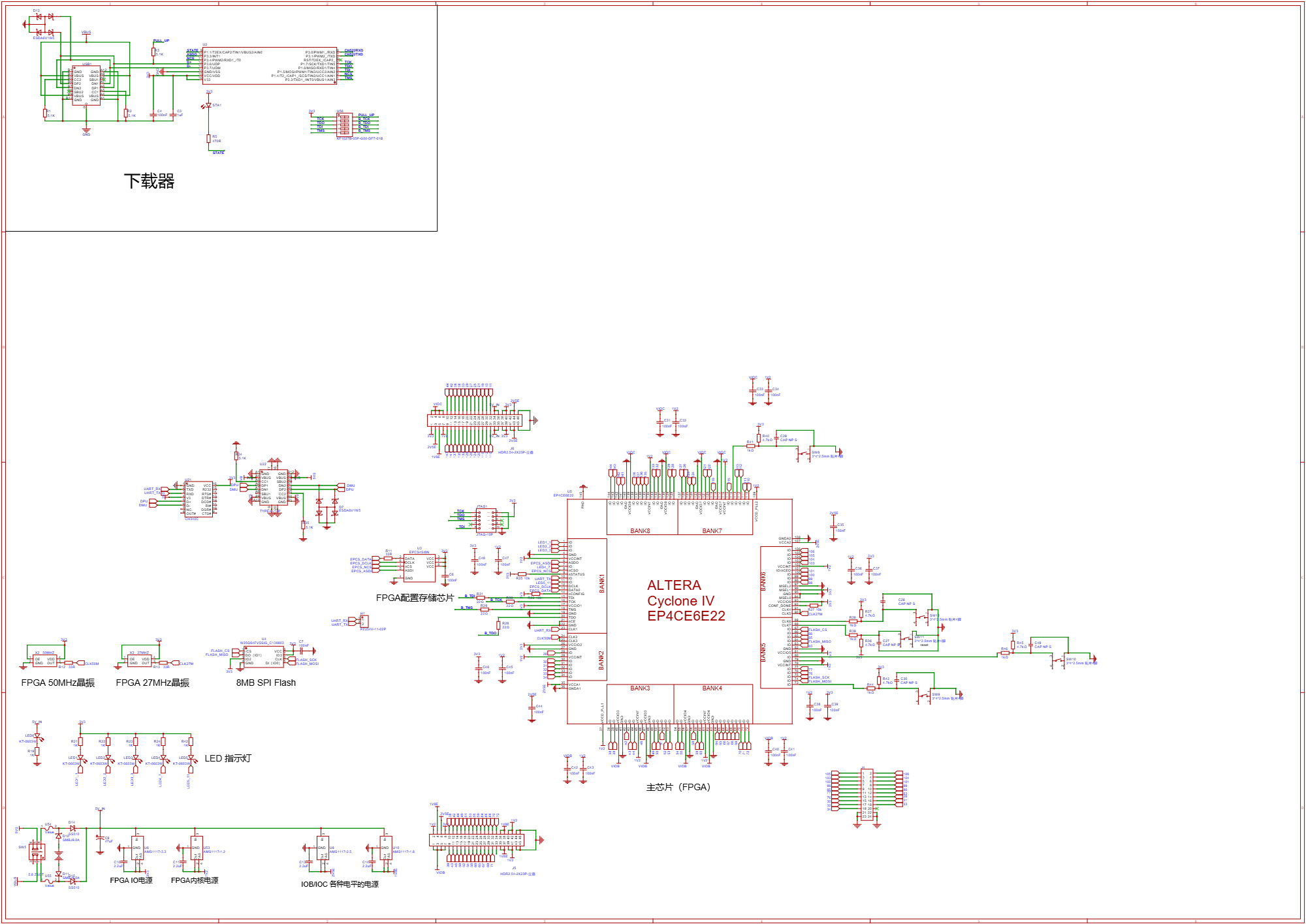
Recently came across the above board and bought one for experiment.
The board contains the following
- EP4CE6E22 Cyclone IV E FPGA in EQFP-144
- 5 LEDs available for the user
- 5 push buttons available
- 50 MHz and 27 MHz clock oscillator
- EPCS4 flash memory for configuration
- W25Q64 memory available for user
- 1.2V, 1.8V, 2.5V and 3.3V regulators for FPGA
- User selectable I/O bank voltage using jumper
- power on/off switch
- JTAG connector for configuration and programming by Byte Blaster
- CH340 USB-TTL connected with FPGA
- Type-C connector for Power Input and acts like USB-TTL
To implement the Z80 CPU core inside the programmable logic device, we need the vendor based IDE for project development.
In this case We need to install the Quartus II package along with modelsim and eclipse tools for NIOS II. The Web edition available from Intel FPGA download site. It is free download and no registration required.
We need atleast Ver 9 or above which supports the Cyclone IV family devices.
We can download anything between 9 to 13 is good enough. Latest version of the software will be huge in size and there is no additional advantage using the latest one.
After installing the Quartus II, we need to download the project file from HERE
Open the project in Quartus II and try compile the source files.
Important thing is the pin assignments. The downloaded project files are meant for different board with different hardware configuration. So we need to re-assign the pins and voltage logic level.
We need the Byte Blaster tool for downloading the SOF file into the target FPGA.
The following video demonstrates step by step how to implement a Z80 Single Board Computer with Z80 CPU, 8kB ROM, 8kB RAM and UART.
The SBC connects with serial terminal at 115200 baud.
There are two I/O ports located at 144 and 145. There are example codes demonstrated to access the port.
There is also demonstration for ASCIIART.
The Quartus 18.1 version Quartus Archive file contains only 4kB RAM. For 8kB we need to download the Quartus 9.1sp2 version Archive file.
All the necessary files are available from the description of the video.
We need USB Blaster to download the SOF or JIC file through JTAG port of the board. SOF file actually configures the FPGA internal RAM and JIC file actually writes the configuration data into EPCS4 FLASH. When we configure the FPGA with SOF file and when we turn off the power, the FPGA loses the configuration data and needs to be configured again.
When we write the JIC file through the JTAG, the configuration data and firmware are written into EPCS4 flash by FPGA. So, every time when we powe up the FPGA, it boots from the EPCS4 flash memory and there are few pins to show the successful configuration of the FPGA.
There are many Clone USB Blasters available at very low cost. Some used STM32 and PIC18F14K50 in the past. But recent clone USB Blasters uses WCH manufactured Enhanced 8051 core based CH552G microcontroller.
It looks something similar to the above image.
I have used the above one.
We can find more information about USB Blaster at the blog HERE
If you do not have a Blaster and yet to buy, then CH552G based is one of the option. It is lowest cost in the clone family and stable.
The above blog explains the firmware update process.
I have updated the default firmware to latest from HERE
We can find the CH552 flash programmer utility from the manufacturer site. We can program through USB port or serial port.
Just connect the 3V3 and USB D+ lines using a jumper just before applying the power. Moment after applying the power, remove the jumper which results in entering into bootload mode.
Tested with Quartus 9, 13 and 18 and works seamlessly.


Comments