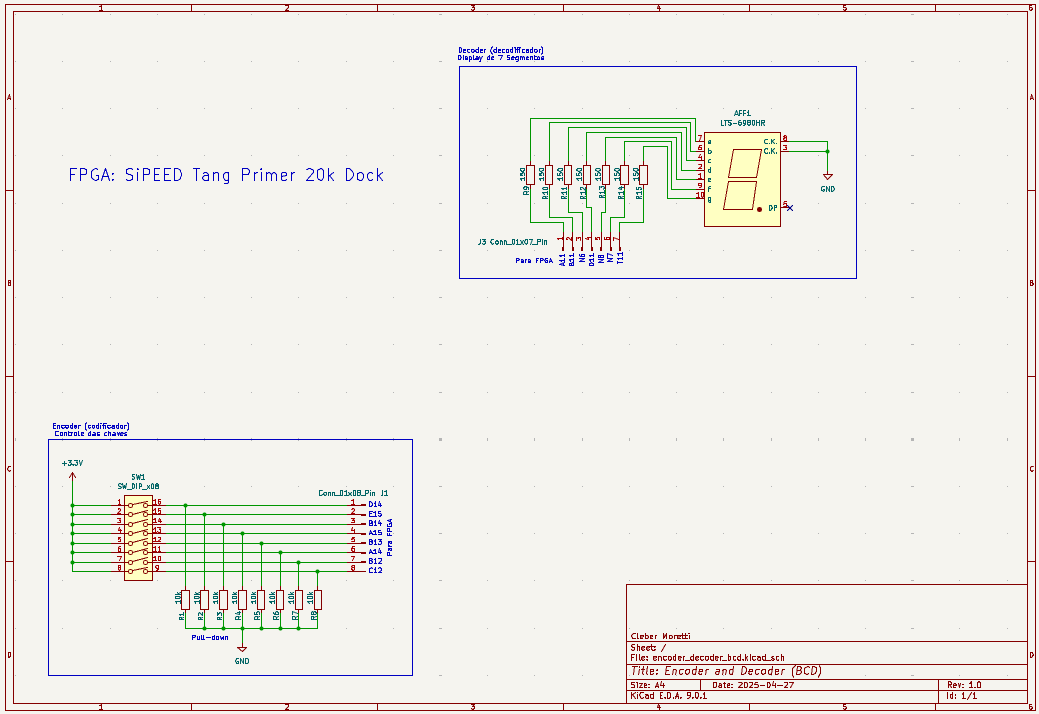
mcleber
Published © GPL3+

7-Segment Display Controller with DIP Switches on FPGA

BCD Decoder and Display Driver using Verilog on FPGA

IntermediateFull instructions provided3 hours94
7-Segment Display Controller with DIP Switches on FPGA

Things used in this project

Hardware components

Tang Primer 20K FPGA (GW2A-LV18PG256C8/I7) with Dock
×1
7 segment display common-cathode
×1
DIP switch 8 position
×1
Resistor 150Ω (current-limiting)
×7
Resistor 10 kΩ (pull-down resistors)
×8
Jumper Wires
×24
Breadboard Full Size
×1
USB Cable Type-C
×1

Software apps and online services

Gowin IDE V1.9.11.01 Education (64-bit)

Story

Read more

Schematics

Schematics

Code

Code

Verilog
//==============================================================================
// Module: encoder_bcd
// 
// Description:
//   This module implements a binary-coded decimal (BCD) to 7-segment display converter
//   with the following functionalities:
//   1. Decodes a cumulative switch pattern into a BCD value
//   2. Converts the BCD value into a 7-segment code (common cathode)
//   3. Handles invalid patterns by displaying 'E' (Error) on the display
//
// Features:
//   - Input: 8-bit binary representing switch states (cumulative pattern)
//   - BCD Output: 4-bit value representing 0-8 or error code (E=1110)
//   - Display Output: 7-bit controlling the segments (0=ON, 1=OFF for common cathode)
//   - Error handling: Any non-cumulative pattern generates an 'E' output
//
// Valid input examples:
//   00000000 (0), 00000001 (1), 00000011 (2), ..., 11111111 (8)
//
// Implemented improvements:
//   1. Simplified module name
//   2. Used always @* for automatic sensitivity
//   3. Expanded documentation
//   4. Improved logical organization
//==============================================================================

`timescale 1ns / 1ps  // Time unit: 1ns, precision: 1ps

module encoder_bcd (
    input      [7:0] switches,           // Binary input (cumulative switch pattern)
    output reg [3:0] bcd_value,          // Converted BCD value (0-8 or E=1110 for error)
    output reg [6:0] display_segments    // Display segments (0=ON, 1=OFF - common cathode)
);

    //==========================================================================
    // Decoding Logic: Cumulative Pattern to BCD
    //
    // Converts cumulative binary patterns (e.g., 00001111) into their numeric
    // equivalents (4 in this case). Non-cumulative patterns trigger an error code ('E').
    //
    // Improvement: Replaced always @(switches) with always @* for automatic sensitivity
    //==========================================================================
    always @* begin
    case (switches)
        8'b00000000: bcd_value = 4'b0000; // 0
        8'b00000001: bcd_value = 4'b0001; // 1
        8'b00000011: bcd_value = 4'b0010; // 2
        8'b00000111: bcd_value = 4'b0011; // 3
        8'b00001111: bcd_value = 4'b0100; // 4
        8'b00011111: bcd_value = 4'b0101; // 5
        8'b00111111: bcd_value = 4'b0110; // 6
        8'b01111111: bcd_value = 4'b0111; // 7
        8'b11111111: bcd_value = 4'b1000; // 8
        default:     bcd_value = 4'b1110; // E (for invalid patterns)
    endcase
end

    //==========================================================================
    // Display Logic: BCD to 7-Segment Conversion
    //
    // Maps the BCD value to the display segments (common cathode).
    // Includes extra mappings (A-F) for potential future expansion.
    //
    // Note: The bit order in the display_segments vector follows the ABCDEFG convention
    //       where bit 6 = segment A, bit 5 = B, ..., bit 0 = G
    //
    // Improvement: Added comment about the segment order
    //==========================================================================
    always @(bcd_value) begin
    case (bcd_value)
        4'b0000: display_segments = 7'b0111111; // 0 (inverted: 1000000  0111111)
        4'b0001: display_segments = 7'b0000110; // 1 (inverted: 1111001  0000110)
        4'b0010: display_segments = 7'b1011011; // 2 (inverted: 0100100  1011011)
        4'b0011: display_segments = 7'b1001111; // 3 (inverted: 0110000  1001111)
        4'b0100: display_segments = 7'b1100110; // 4 (inverted: 0011001  1100110)
        4'b0101: display_segments = 7'b1101101; // 5 (inverted: 0010010  1101101)
        4'b0110: display_segments = 7'b1111101; // 6 (inverted: 0000010  1111101)
        4'b0111: display_segments = 7'b0000111; // 7 (inverted: 1111000  0000111)
        4'b1000: display_segments = 7'b1111111; // 8 (inverted: 0000000  1111111)
        4'b1110: display_segments = 7'b1111001; // E (inverted: 0000110  1111001)
        default: display_segments = 7'b0111111; // Default (off)
    endcase
end

endmodule

Constraints

Textile
Constraints for Tang Primer 20K + Dock
//Copyright (C)2014-2025 Gowin Semiconductor Corporation.
//All rights reserved. 
//File Title: Physical Constraints file
//Tool Version: V1.9.11.01 Education (64-bit)
//Part Number: GW2A-LV18PG256C8/I7
//Device: GW2A-18
//Device Version: C
//Created Time: Sun 05 04 15:11:17 2025

IO_LOC "display_segments[6]" T11;
IO_PORT "display_segments[6]" IO_TYPE=LVCMOS18 PULL_MODE=UP DRIVE=8 BANK_VCCIO=1.8;
IO_LOC "display_segments[5]" N7;
IO_PORT "display_segments[5]" IO_TYPE=LVCMOS18 PULL_MODE=UP DRIVE=8 BANK_VCCIO=1.8;
IO_LOC "display_segments[4]" N8;
IO_PORT "display_segments[4]" IO_TYPE=LVCMOS18 PULL_MODE=UP DRIVE=8 BANK_VCCIO=1.8;
IO_LOC "display_segments[3]" D11;
IO_PORT "display_segments[3]" IO_TYPE=LVCMOS18 PULL_MODE=UP DRIVE=8 BANK_VCCIO=1.8;
IO_LOC "display_segments[2]" N6;
IO_PORT "display_segments[2]" IO_TYPE=LVCMOS18 PULL_MODE=UP DRIVE=8 BANK_VCCIO=1.8;
IO_LOC "display_segments[1]" B11;
IO_PORT "display_segments[1]" IO_TYPE=LVCMOS18 PULL_MODE=UP DRIVE=8 BANK_VCCIO=1.8;
IO_LOC "display_segments[0]" A11;
IO_PORT "display_segments[0]" IO_TYPE=LVCMOS18 PULL_MODE=UP DRIVE=8 BANK_VCCIO=1.8;
IO_LOC "switches[7]" C12;
IO_PORT "switches[7]" IO_TYPE=LVCMOS18 PULL_MODE=DOWN BANK_VCCIO=1.8;
IO_LOC "switches[6]" B12;
IO_PORT "switches[6]" IO_TYPE=LVCMOS18 PULL_MODE=DOWN BANK_VCCIO=1.8;
IO_LOC "switches[5]" A14;
IO_PORT "switches[5]" IO_TYPE=LVCMOS18 PULL_MODE=DOWN BANK_VCCIO=1.8;
IO_LOC "switches[4]" B13;
IO_PORT "switches[4]" IO_TYPE=LVCMOS18 PULL_MODE=DOWN BANK_VCCIO=1.8;
IO_LOC "switches[3]" A15;
IO_PORT "switches[3]" IO_TYPE=LVCMOS18 PULL_MODE=DOWN BANK_VCCIO=1.8;
IO_LOC "switches[2]" B14;
IO_PORT "switches[2]" IO_TYPE=LVCMOS18 PULL_MODE=DOWN BANK_VCCIO=1.8;
IO_LOC "switches[1]" E15;
IO_PORT "switches[1]" IO_TYPE=LVCMOS18 PULL_MODE=DOWN BANK_VCCIO=1.8;
IO_LOC "switches[0]" D14;
IO_PORT "switches[0]" IO_TYPE=LVCMOS18 PULL_MODE=DOWN BANK_VCCIO=1.8;

Credits

mcleber
5 projects • 0 followers
Enthusiast in FPGA, Computer Vision and Machine Learning.

Comments