

Hardware components | ||||||
 |
| × | 1 | |||
| × | 1 | ||||
| × | 3 | ||||
| × | 1 | ||||
| × | 1 | ||||
 |
| × | 1 | |||
 |
| × | 3 | |||
 |
| × | 3 | |||
| × | 1 | ||||
| × | 1 | ||||
| × | 1 | ||||
Software apps and online services | ||||||
| ||||||
| ||||||
| ||||||
Hand tools and fabrication machines | ||||||
 |
| |||||
| ||||||
| ||||||
This project presents a Secure Digital Access Control System built using a Finite State Machine (FSM) on the DE1-SoC FPGA board. The system allows users to enter a 4-digit password through a keypad or switches, verifies the password in hardware, and provides feedback through LEDs, 7-segment displays, a TFT screen, and a buzzer. To improve security, the system includes an inactivity timeout and a 15-second lockout mechanism after three failed attempts. The complete hardware is assembled inside a custom 3D-printed enclosure, making it a practical FPGA-based prototype for access control applications.
1 Why I Built ThisThis project was originally developed as part of my Logic System Design assignment, where the task was to design a real-world embedded control system using a Finite State Machine and synthesizable Verilog HDL. I chose to build a Secure Digital Access Control System because it is a practical security application that clearly shows how digital logic can be used to control password entry, access verification, failed attempts, timeout, and lockout behaviour.
Instead of only completing the design in simulation, I wanted to make the project more meaningful by implementing it on real FPGA hardware using the DE1-SoC development board. The system allows a user to enter a 4-digit password, checks whether the password is correct, gives feedback through LEDs, 7-segment displays, a TFT display, and a buzzer, and activates a 15-second lockout after three failed attempts. This made the assignment more than just a theory-based FSM design, because the final result became a working access control prototype that can be tested and demonstrated physically.
2 Project ObjectivesThe main objective of this project is to design and implement a Secure Digital Access Control System using the DE1-SoC FPGA board. The system is developed to demonstrate how a Finite State Machine can be used to control a real-world security application, where each input, output, and system response must operate in a reliable and organized way.
The project aims to create a 4-digit password entry system that can verify whether the entered password is correct or incorrect. The password can be entered through the keypad, slide switches, or buttons, while the entered digits are shown on the 7-segment display and duplicated on the TFT display for clearer user feedback.
Another objective is to improve the security and usability of the system by adding important protection features, such as inactivity timeout, failed-attempt counting, buzzer feedback, LED status indication, and a 15-second lockout mechanism after three failed attempts. These features help make the system more practical and closer to a real access control application.
3 DE1-SoC FPGA Board OverviewThe DE1-SoC FPGA Board is a powerful embedded development system platform that is developed to support embedded applications and digital system design. It is designed based on the Altera System-on-Chip (SoC) FPGA that combines a dual-core ARM Cortex-A9processor with programmable logic on a single chip. This integration enables designers to integrate hardware as well as software capabilities in a single system with high flexibility and performance. The board uses a 12V power adapter and communicates with a computer via a USB Type-A to Type-B cable allowing it to be easily programmed and debugged via the onboard USB-Blaster II interface in JTAG mode. Figure 1 shows the DE1-SoC FPGA board.
Figure 2 shows the device numbering of Cyclone V.
Regarding physical layout, the board has a large variety of onboard components, as depicted in Figure 3 (top view) and Figure 4 (bottom view). These models depict the position of connectors, interfaces, and other important hardware components that facilitate the development of the system. The board is divided into two major sections, the FPGA (programmable logic) part and the Hard Processor System (HPS) part, which offer various functions to implement the system.
The FPGA section relies on the Altera Cyclone5CSEMA5F31C6N device and features a few critical hardware features which assist in the design and testing of digital designs:
· USB-Blaster II for FPGA configuration using JTAG mode
· 64MB SDRAM with a 16-bit data bus
· Four pushbuttons and ten slide switches for user input
· Ten red user LEDs and six 7-segment displays for output indication
· Four 50 MHz clock sources from the onboard clock generator
· Two 40-pin GPIO expansion headers with diode protection circuitry
· An A/D converter with a 4-pin SPI interface
Moreover, embedded processing is offered in the HPS section by utilizing the ARM-based processor and the peripherals:
· 800 MHz dual-core ARM Cortex-A9 MPCore processor
· 1GB DDR3 SDRAM with a 32-bit data bus
· Gigabit Ethernet interface with RJ45 connector
· Two USB host ports (Type-A)
· Micro SD card slot for storage
· Accelerometer with I2C interface and interrupt support
· UART-to-USB interface using a USB Mini-B connector
· Warm reset and cold reset buttons
· One user button and one user LED
· LTC 2×7 expansion header
The DE1-SoC board is a full and highly integrated hardware platform that is useful in both logic design and embedded system development on an FPGA. Its ability to have extensive onboard peripherals, input/output interfaces and expandability make it very appropriate in the implementation of complex systems like the FSM-based secure digital access control system that was created in this project.
4 Block Diagram of the DE1-SoC BoardThe block diagram of the DE1-SoC FPGA Board is given in Figure 5, which depicts the connection between all the parts of the system with each other through the core Cyclone V SoC FPGA core. It is highly flexible architecture, with the FPGA being programmable to allow users to build their own digital systems as well as making use of the embedded processor to carry out more complex control and processing endeavours. In general, the block diagram shows a highly integrated system in which all the elements are linked to each other via the Cyclone V SoC.
5 GPIO Expansion Header OverviewThe DE1-SoC FPGA Board has several GPIO expansion headers that can be used to connect the external peripherals, as shown in Figure 6. The board offers 2 40-pin expansion headers of the GPIO, each header has 36 customizable I/O pins which connect directly with the Cyclone V SoC FPGA. Besides these data pins, additional per-header connections are also present, specifically, power supply connections, i.e., +5V (VCC5) and +3.3V (VCC3P3) and ground (GND) connections. The power pins can be connected directly to external devices like displays, keypads and sensors and provide a simplified hardware configuration. The amount of current carried on these supply lines, however, must be attended to. The 5V supply should have a maximum of 1A and the 3.3V supply should have a maximum of 1.5A, which makes sure that any external hardware it is connected to does not operate beyond safe operating currents.
All the GPIOs are not exposed directly and are linked together by a series resistor and clamped by a set of diodes connected to the 3.3 V supply and ground. This protection circuit is useful in protecting the FPGA against spikes in voltage or improper signal levels. Should more than 3.3V be accidentally applied, the diode across VCC3P3 will conduct and limit the voltage, with negative voltages limited to ground by the other diode. The series resistor also limits the current into the FPGA pin, which diminishes the chances of the pin being damaged. This layout makes the GPIO pins strong and, when used with other modules, they can safely communicate with them, as long as appropriate voltage levels are observed.
In general, the GPIO expansion headers provide flexibility and protection to the FPGA as the primary interface with the peripherals.
6 Methodology6.1 Block Diagram of the Overall Hardware ArchitectureFigure 7 shows the block diagram of the overall hardware architecture. The block diagram shows how all the input and output components are connected to the DE1-SoC FPGA Board to create the complete Secure Digital Access Control System. The FPGA board is located at the core of the system and serves as the principal processing unit, processing all the inputs, implementing the control logic based on the FSM, and producing the appropriate outputs. On the input end, there are several devices attached to the FPGA as the 4x4 keypad, onboard switches, onboard pushbuttons and three external buttons. These input devices enable the user to input the password, verify or clear input and reset the system. The keypad and the switches are primarily used to input the digits whereas the buttons are used to do control functions like confirmation and system reset.
The FPGA drives a number of display and indication devices on the output side. The 7-segment onboard displays are made to display the entered password digits giving the user instant visual feedback. Besides this, a 3.5-inch TFT display is also attached that displays more detailed information about the system like status messages. An active buzzer is also provided as an output device to offer audio cues especially when the wrong password is entered or when the system gets locked out.
A 12V power supply is used to power the system, and it is connected to the FPGA board to provide a stable operation of all components. In addition, a laptop with Quartus II software is used with the FPGA using a USB interface. This connection is utilized to program the FPGA, upload the Verilog design and debug or test the development.
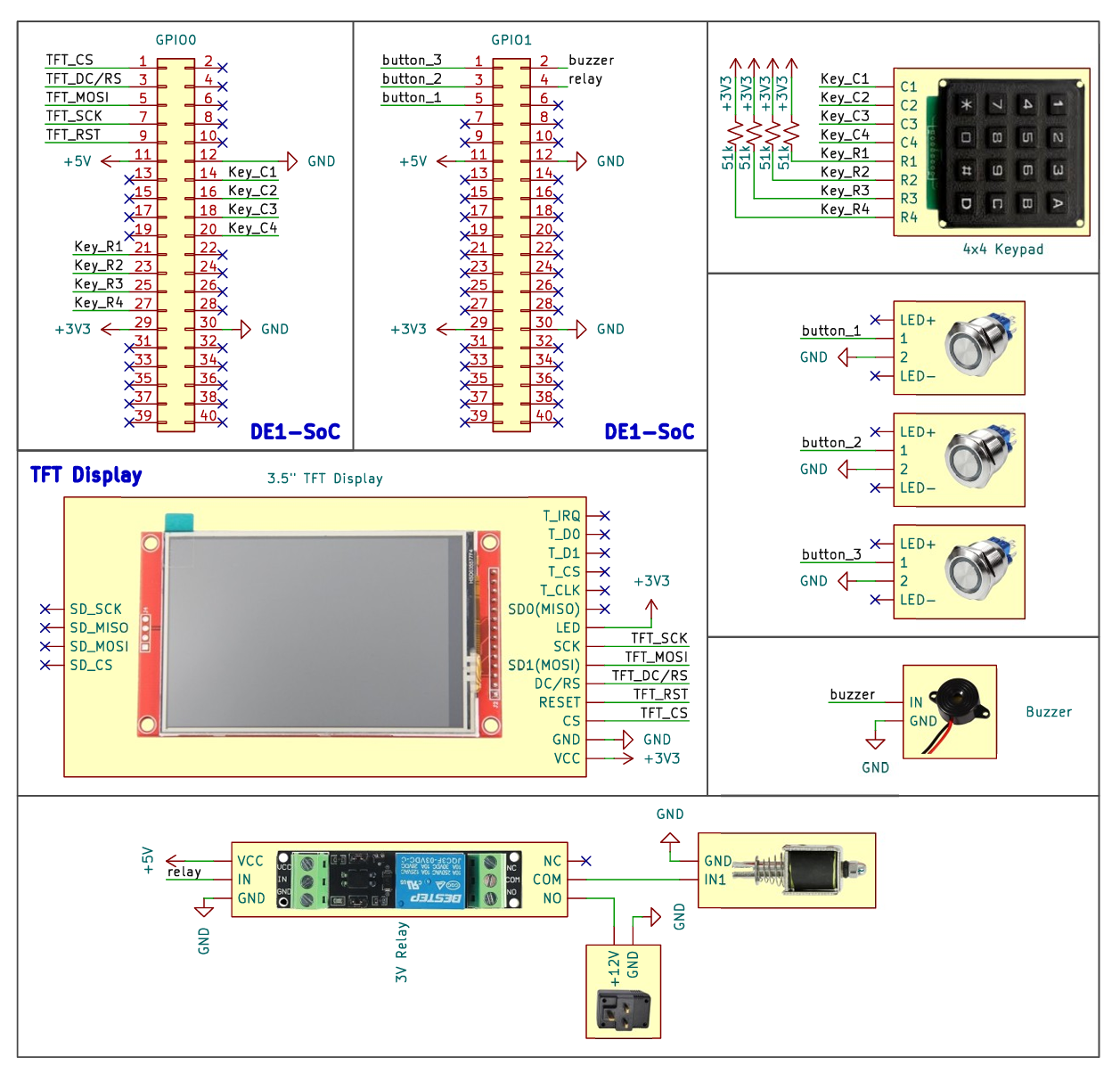
6.2 Schematic Diagram of External PeripheralsFigure 8 shows the schematic diagram of external peripherals. The schematic diagram shows the physical implementation of the Secure Digital Access Control System in the DE1-SoC FPGA Board, where all the external components are interconnected via the helper expansion GPIO0 and GPIO1 head. Starting with GPIO0, this header is mainly used for user interaction devices, which include the TFT display and the 4×4 keypad. In the case of the TFT display (3.5-inch TFT) multiple specific GPIO pins are allocated to communicate using SPI. In particular, the TFT_CS (chip select), TFT_DC (data/command selection), TFT_MOSI (data input), TFT_SCK (clock), TFT_LED (backlight control) and TFT_RST (reset) signals are wired to different GPIO0 signal lines. These interconnections enable the FPGA to transmit commands and graphical data to the display so that it can display messages like password input or access granted or error messages. There is also a clear definition of power connections, with display VCC being connected to +3.3V and GND to the board ground, to make sure the operation is stable.
The 4×4 keypad is also connected via a matrix set up comprising eight signal lines in the same GPIO0 header. Key R1, Key R2, Key R3, and Key R4 are used as the row lines and Key C1, Key C2, Key C3, and Key C4 are used as the column lines. All these lines are assigned to a corresponding GPIO0 pin. The FPGA manages the keypad by pushing the row lines and reading the column lines, enabling it to sense the key pressed. This scanning technique is effective and minimizes the number of pins needed but still enables the 16 keys.
Moving to GPIO1, this header is used as the control input and output alerts. External metal push buttons, labelled as button1, button2 and button3, are connected to different GPIO1 pins. On each button, one of the terminals is connected to a GPIO pin and the other to ground, and pull-up resistors are used to ensure that the default state is stable when the button is not being pressed. Specific control functions like system reset, password entry confirmation or special mode triggering are done with these buttons. Also, there is an active buzzer attached to GPIO1 with a control pin attached to a GPIO output pin and the ground attached to GND. This pin leads to the buzzer producing a sound when the FPGA sends a HIGH signal to it, and thus the user receives instant audio feedback, e.g. notifications of an incorrect password or lockout.
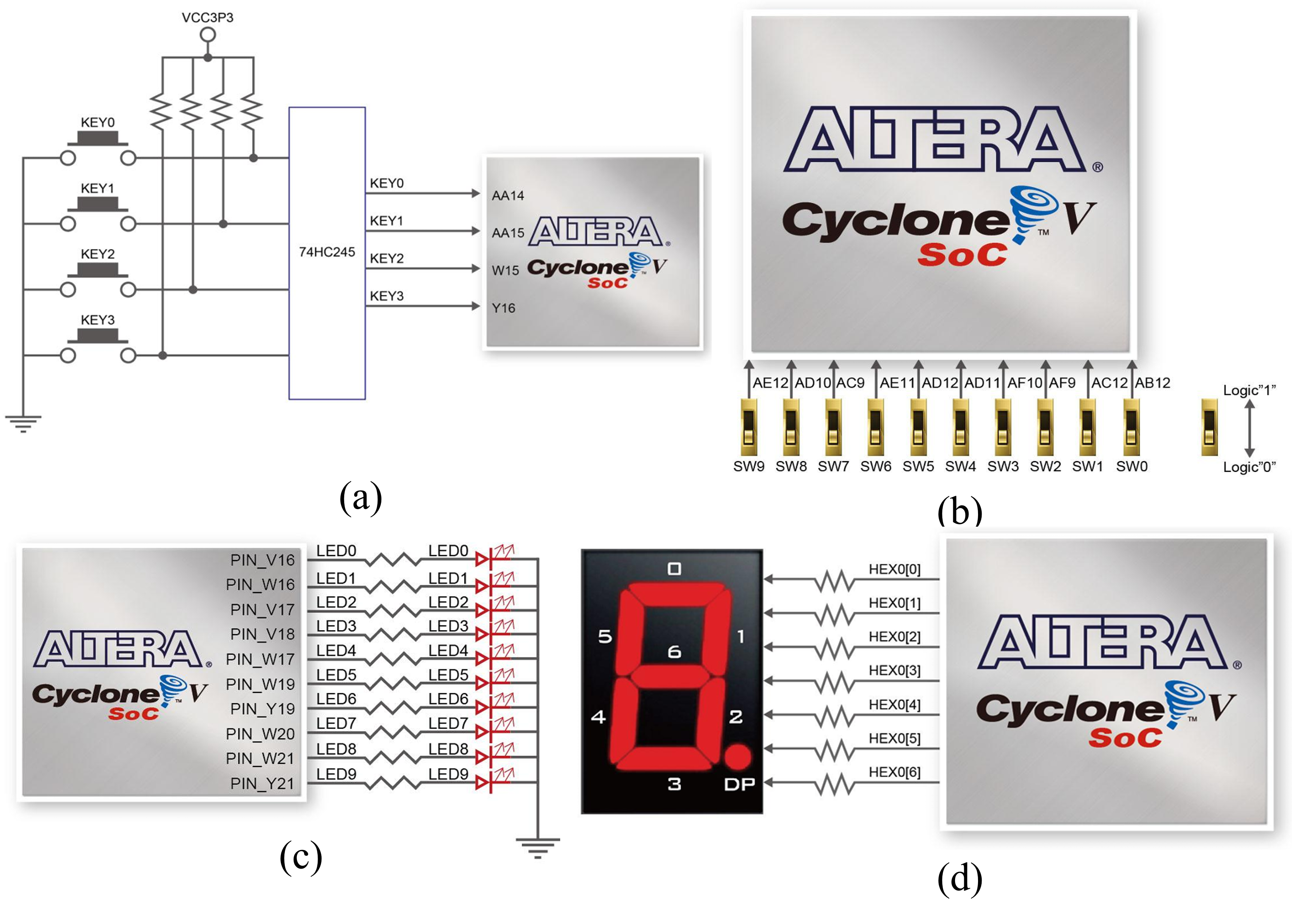
6.3 Summary of Pinout Assignment of External PeripheralsFigure 9 shows the schematic diagram of on-board peripherals and displays. In addition to the external components, the design also utilizes selected onboard peripherals of the DE1-SoC FPGA Board to support and replicate the system functionality. Key 0, Key 1 and Key 2 Onboard pushbuttons KEY0, KEY1 and KEY2 are internally linked to FPGA pins AA14, AA15, and W15 via a 74HC245 buffer and a Schmitt trigger circuit, which offers hardware debouncing and stable signal transitions. These push-buttons are active-low, i.e. a logic 0 is produced when in the pressed state, and a logic 1 when in the released state. In this system, KEY0 is the confirm button to confirm the typed in 4-digit password, KEY1 is the clear button to clear all the characters typed so far and KEY2 is the full system reset button that clears the typed password and the wrong attempt counter. The Schmitt trigger is added so that mechanical noise of the button presses does not lead to the unwanted multiple triggers.
Onboard slide switches SW0 to SW9 directly connect to pins in the FPGA like AB12, AC12, AF9, AF10, AD11, AD12, AE11, AC9, AD10 and AE12. These switches are debounced, and level sensitive. The switches are binary input with the UP position generating a logic 1 and the DOWN position generating a logic 0. The switches in this design are utilized in the representation of digits 0 to 9 which offers another way of typing the password instead of using the external keypad. This is a very handy feature when it is time to test and debug.
To indicate output, they use five onboard LEDs (LED0 to LED4) that are directly connected to the FPGA pins of V16, W16, V17, V18 and W17. These LEDs are active-high i.e. they become ON when logic 1 is supplied to them. The LED0 means that the system is in idle or locked position and LED1 means that access is successful when the right password is typed in at this point LED0 is switched off. LED2, LED3, and LED4 are used to show the number of bad passwords attempted: LED2 is turned on after the first attempt, LED2 and LED3 are on after the second attempt, and LED2, LED3, and LED4 are on after the third attempt. Reaching the third attempt the buzzer is also set off to enable audible warning to the security feedback of the system.
Moreover, the system incorporates four onboard 7-segment displays (HEX0-HEX3) which display the typed password digits. Each display has seven segments, denoted HEXx[0] to HEXx[6], driven out to FPGA output pins by current-limiting resistors. These displays are programmed to be common anode, i.e. a logic 0 causes a segment to be ON and a logic 1 causes it to be OFF. The figures are presented in the order, HEX3 indicates the first figure typed, and HEX0 indicates the last typed figure. This layout presents real-time and visual feedback to the user when typing in passwords.
Overall, the schematic depicts a logical and convenient hardware design. GPIO0 is reserved to components with high interaction such as display and keypad whereas GPS1 deals with simpler control inputs and output indicators. The flexibility and usefulness of the system are improved through the use of the chosen onboard components to offer alternative ways of input and output. This enables the system to be tested and run even in the absence of external peripherals yet provides stable signal processing and easy integration with the FSM-based control logic running in the FPGA.
6.5 Summary of Pinout Assignment of On-Board Peripherals and DisplaysFigure 10 shows the 3D Enclosure Design of the Secure Digital Access Control System. The 3D design was created in Autodesk Fusion to offer a compact, systematic and easy to operate housings to all the system components. The size of the enclosure is 160.88 mm x 178 mm x 85.8 mm, which is planned to be large enough to fit the DE1-SoC FPGA Board, together with all external peripherals. The enclosure is split into two parts with the top part (front) and the back part. The front side is made to accommodate the user interface, such as the TFT display, the keypad and three external buttons, and the back section will be used to firmly fit the FPGA board. The internal layout is planned to ensure the FPGA is tightly fitted inside the enclosure without any further mounting distance, enabling the system to be stable with a simple and compact design.
Figure 11 shows the dimension drawing of the 3D enclosure design while Figure 12 shows the 3D enclosure design with component layout. A filament hinge system is also included within the enclosure, involving a 1.75 mm filament directly fitted into the enclosure to serve as a flexible hinge to ensure the two portions of the enclosure can open and close easily. This design does not need any more mechanical hinges and is easy to assemble. Three circles are created on the front panel and located at the top to accommodate the external buttons, and a bigger rectangular opening is made to accommodate the TFT display. Under the display, there is another cutout which will accommodate the keypad so that all the user input and output sections can be easily reachable. Also, it has a side opening to fit a lock opener mechanism, which enables the solenoid lock to be manually activated when debugging or troubleshooting. This is especially helpful to safely open the enclosure to access internal wiring without the need to use the electronic control system.
Overall, the design of the enclosure puts emphasis on practicality, ease of use and integration. Using all the components in one compact design with correct positioning of input and output interfaces the design guarantees effective user interaction and safeguards the internal hardware.
6.7 3D PrintingThe enclosure of the Secure Digital Access Control System was designed and manufactured by a fused deposition modelling (FDM) 3D printing technology, which offers low cost and efficient solution to creating customized hardware enclosures. This enclosure was 3D printed in Cherry Blossom Pink PETG filament, which was chosen due to its durability, a bit of flexibility, and enhanced heat resistance over the standard PLA materials. Printing was separated into two major sections which were the top and bottom parts of the enclosure. The top part has an approximate weight of 95g, while the bottom part weighs about 143g. The Fuzzy skin method was used on the outer shape of the case. This method provides a slightly textured finish on purpose and in this way minimizes the visibility of layer lines that are usually observed in FDM printing. Consequently, the resulting printed enclosure looks cleaner, and more like a finished product.
Figure 14 shows the assembled hardware. The completed hardware can then be used to assemble all the designed components in a small functional enclosure to create a complete Secure Digital Access Control System. The enclosure consists of two primary parts, the right side contains the DE1-SoC FPGA board, and the left side contains the support circuitry, the breadboard, solenoid lock mechanism and active buzzer. The FPGA board is firmly fixed to allow stability, and the GPIO0 and GPIO1 headers are linked using ribbon cables to allow the connection of the external hardware, 4x4 keypad, TFT display and external pushbuttons.
In general, the complete system is a well-structured and realistic implementation of hardware. The system is lightweight, and its total weight is about 700g.
6.9 Configuration of Cyclone V SoC FPGA on DE1-SoCThe Cyclone V SoC FPGA configuration of the DE1-SoC FPGA Board is a necessary procedure to load the designed digital system to the hardware. The board has two major programming methods, which are JTAG programming and Active Serial (AS) programming. With JTAG programming, the resulting bitstream of the configuration is directly downloaded into the FPGA via the onboard USB-Blaster II interface. This is an easy approach and most commonly used in the development process since it enables rapid testing and debugging. The configuration can however be volatile, i.e., the programmed data will be lost as soon as the power supply is switched off, and it will require reprogramming the FPGA each time the board is turned on.
The JTAG programming technique is employed in this project because it is convenient when developing and testing. The setup procedure is based on the well-constructed JTAG chain that serves as a communication channel between the computer and the FPGA. Figure 15 shows how the JTAG chain connects to the USB-Blaster II connector, through the Cypress CY7C68013A interface, through the MAX II device (EPM570GF100) and to the Cyclone V SoC FPGA.
The general system flow diagram illustrates the entire process of operation of the Secure Digital Access Control System beginning with power-up to user interaction and the end result outputs. The flow gives a clear and organized picture of how the various modules within the system interact with each other, such as the input handling, data processing, state control, and output generation.
Upon booting, the system goes through an initializing phase during which it waits a moment (about 1.3 ms) before it can be certain that all hardware components and signals are stable. After the system has been initialized it passes into a ready state, waiting until the user interacts with the system. In case the reset button is pressed at some point, the system will re-initiate this process.
Once the system is in place, it is always checking various input sources like the 4x4 keypad, slide switches and push buttons. The keypad works on a scanning system, in which rows and columns are scanned one after the other, to identify the key being pressed. The slide switches can also be used as another input method since it directly shows the digit selected whereas the push buttons are used to do control functions like submit and clear. As soon as a valid input is detected, the system marks it as a digit entry and proceeds to the next stage.
The digit storage module is the module that processes all the inputs. Upon the clear button being pressed, all the digits stored are undone, and the user can begin the process of input again. In cases where numbers are typed in, they get saved in consecutive order, up to four numbers. On pressing the submit button, the system analyses the numbers typed. When the 4-digit password is used correctly, it is granted access, and the door opens. In case of an incorrect password, the access is denied, and the counter of failed attempts is increased. Once three failed attempts have been made, the system goes into lockout, during which any further input is temporarily disabled (15 seconds).
Besides password checking, the system has an idle timer mechanism to enhance reliability and usability. In case the user is inactive, the timer is reset when he/she is active. When there is no input within a given time (e.g. 10 seconds), the system will automatically delete the typed numbers. In case of inactivity, a system is set to enter a state of time-out, so that half-finished or unfinished inputs do not have to be stored. The system implements a delay during lockout and then permits further interaction, which is more secure.
The FSM is the heart of this system that manages all the operations with the help of the Moore machine setup consisting of seven states: IDLE, ENTRY, VERIFY, GRANTED, DENIED, LOCKOUT and TIMEOUT. The FSM specifies the manner in which the system makes the state changes according to the input condition and internal signals. To illustrate, a digit is pressed the system will change to ENTRY, the submit button is pressed, the system changes to VERIFY, and based on the outcome, the system will change to either GRANTED or DENIED. Transition to TIMEOUT and LOCKOUT states are triggered by special conditions like inactivity and repeated failures, respectively. Once each operation is done, the system goes back to the IDLE state to be ready to do the next cycle.
Lastly, the system produces outputs depending on the state at hand. The buzzer gives audio feedback, with varying sounds when access is successful, incorrect attempts, time out and clear. The LED indicators show the status of the system, e.g. locked, unlocked, and the number of failed attempts. Visual feedback is included in the 7-segment displays and TFT screen, which displays the digits typed in real time.
6.11 State TableThe Secure Digital Access Control System has a control subsystem, which is implemented based on a MooreFinite State Machine (FSM) architecture. The outputs in a Moore machine are only influenced by the existing state and not the input signals, which enhances better stability in a system and eliminates glitches during input transitions.
FSM has seven states (S0, S1, S2, S3, S4, S5, S6): IDLE (S0), ENTRY (S1), VERIFY (S2), GRANTED (S3), DENIED (S4), LOCKOUT (S5), and TIMEOUT (S6). Every state is a distinct phase of system work, waiting until a user activates the system, authentication findings, and security measures. The system starts at the IDLE state and switches between states depending on conditioned input signals like key_valid, submit request, clear request and inactivity-timeout which guarantee structured and controlled system behaviour.
The states are represented in binary and one-hot encoding pattern to facilitate FPGA implementation and address engineering constraints. One-hot encoding has been chosen to be implemented because it provides a faster decoding process and less complicated combinational logic, enhancing timing performance of FPGA hardware.
The state transition table is a table of all possible transitions between states depending on input conditions. As an example, the system only switches to VERIFY after a submit request has been detected, which means that unfinished inputs are not processed. Likewise, the switch to LOCKOUT is only made upon the third failure, which implements the security constraint. The TIMEOUT condition is activated in case of the inactivity, where the unattended inputs are not left in the system. These transitions are also formulated to prevent cases of invalid states, deadlock and unintended loops.
Output table has characteristics of Moore machine with outputs like grant pulse, deny pulse and timeout pulse being produced based on the current state only. As an example, the GRANTED state sets the unlock signal, the DENIED and TIMEOUT states send the feedback signals. The other states do not produce any output, with clean and controlled system responses.
It provides secure password validation, a lockout after three unsuccessful attempts and inactivity time functionality.
The FSM is closely interacting with other modules within the system. The input conditioning module provides a stable signal prior to the FSM being fed, the datapath module stores and compares passwords, and the output control module produces a visual and audio signal depending on the FSM state. This synchronized communication reflects the system-level integration necessary in the real-world digital design.
7 Results & Discussions7.1 SimulationModelSim was used to simulate the Secure Digital Access Control System to ensure that the system was functionally correct in the implemented FSM-based design before being implemented in hardware. The overall simulation duration will be 4500ns and the waveform will be split into five parts to enable easy analysis of the behaviour of the system in various phases. The simulation environment is also ideal unlike real hardware testing that does not involve physical effects like switch bouncing, signal noise or wiring delays. Thus, the simulation is completely aimed at the verification of the logical functionality of the FSM, datapath, and interactions between modules under controlled conditions.
Figure 18 shows the simulation waveform from 0ns to 900ns. Initialization of the system takes place at the start of the simulation (0 ns to 900 ns). The reset signal makes sure that the internal registers such as the digit registers, attempt counter and state register are cleared. In this phase, the FSM is at the IDLE state with no output signals, including grant pulse, deny pulse and the timeout pulse, being triggered.
Figure 19 shows the simulation waveform from 900ns to 1800ns. In the following part of the waveform, the system starts to do user input. The digit_valid signal is turned on, and digit_value signals are monitored, which means that the digits are being typed into the system via the testbench. When each valid input is received, the FSM switches to the ENTRY state, the digits are stored sequentially in the datapath. The number counter goes up as well.
Figure 20 shows the simulation waveform from 1800ns to 2700ns. The submit signal is received as the simulation continues, which causes the ENTRY state to be changed to the VERIFY state. At this level, the Datapath will match the entered 4-digit sequence and with the programmed password. The waveform indicates that this comparison is done right, and the outcome of the comparison is the subsequent state transition. In case the typed password is identical to the stored password, the FSM transitions to the GRANTED state, and the grant-pulse signal is sent. This will mean successful authentication. When the password is not correct, the FSM switches to the DENIED state, and the deny pulse signal is sent, and the counter of attempts is increased.
Figure 21 shows the simulation waveform from 2700ns to 3600ns. Further into the simulation, repeated incorrect password entries are applied to test the system’s security features. As seen in the waveform, every time the attempt is at the maximum limit of three attempts and fails, the attempt counter is incremented, and once it reaches the maximum threshold, the FSM moves to the LOCKOUT state. All input signals are actually ignored in this state, and no additional operations can be done until the lockout period has passed.
Figure 22 shows the simulation waveform from 3600ns to 4500ns. Besides lockout feature, the simulation also tests inactivity timing mechanism. In the event of the absence of input activity during a predefined time period, the system goes to the TIMEOUT state. In this state, the timeout-pulse signal is triggered, and all the partially entered digits are cleared out of the Datapath. Following the occurrence of the timeout event, the FSM goes back to the IDLE state and is ready to start a new input cycle.
The DE1-SoC FPGA board was used to hardware test the Secure Digital Access Control System to test the real-time functionality of the implemented Verilog design. The system works based on the targeted FSM and Datapath behaviour in which user inputs are received, checked.
When the system is at the first state, LEDR0 is turned on, and the system is in a locked state. In testing, various input methods are verified to be working properly. The system takes input not only the onboard slide switches, but also the external 4×4 keypad. As Figure 23 (b) illustrates, when switch ON SW5, the 7-segment display effectually displays digit 5, and when pressing a key on the keypad, the same digit is displayed. This shows both the input sources are properly integrated and mapped in the system. The external pushbuttons also serve the same purposes as the onboard KEY buttons, where they are utilized in confirm, clear and reset functions giving the user flexibility in interacting with the system.
Each digit is entered in a particular sequence and as shown in Figure 24 (c) all the digits entered are shown clearly in all the 7 segment displays. Meanwhile, the TFT display is able to replicate the typed password, which is another visual interface to the user. This two-screen system makes the interface more user-friendly as it enables users to confirm their input more easily.
Once the confirm button is hit, the system will then proceed with verifying the password typed in. In case the password is right the system switches to unlocked state, such that LEDR1 is on and LEDR0 off. In case of an incorrect password, the system will be left in the locked condition with LEDR0 on. The system is automatically cleared of the entered digits after verification in both cases and the system is ready to take a new input cycle. This makes every authentication attempt a fresh start with no residual information.
The system also shows that there is a proper management of failed attempts and security. With every wrong password a buzzer is triggered, and the failed attempt counter is increased, and this is shown by LEDR2, LEDR3, and LEDR4. When the system makes three unsuccessful attempts, it deactivates the system and opens a lockout system in which no input is taken in the period of about 15 seconds. This is to assure that the protection mechanism is operating properly and improves the overall system security.
Moreover, the inactivity time option is effectively tested. When the user types of numbers and fails to complete the transaction within some time frame, the system automatically erases the typing and creates a sound of a buzzer. This will ensure that incomplete entries are not stored in the system and enhance reliability. The system is also more user friendly as the buzzer also gives feedback on various events like wrong attempts and time out.
Overall, the hardware testing proves that the system works with the required stability and corresponds to the design requirements. A combination of various input modes (switches and keypad), duplicate display (7-segment and TFT) and uniform control with onboard and external buttons all testify to a well-defined and versatile system. All major features such as digit entry, password verification, automatic clearing, inactivity time, buzzer feedback, the 15-second lockout after three failed attempts are all working well in real hardware implementation.
7.3 Video Demonstration7.4 Hardware LimitationsAccording to the hardware test results, the system can fulfil its desired functions with high level of reliability but there are a number of practical limitations noted during the actual hardware implementation. These constraints are primarily associated with the physical, user interaction, and real-time behaviour of the system.
The response time and input stability when the external keypad is used is one of the main constraints. The keypad works but with rapid key presses, there might be small delays or inconsistencies caused by signal scanning and debouncing limitations. This can sometimes have some impact on user experience, particularly where entering digits are required in a hurry. The onboard slide switches, in comparison, have more stable inputs, but are less real-world friendly.
From a hardware integration perspective, the use of multiple wired connections between the FPGA board, keypad, TFT display, and other peripherals introduces potential issues such as loose connections or signal noise, especially when placed inside the enclosure. Although the system operates correctly during testing, long-term usage may require more robust wiring or PCB integration for improved reliability.
Lastly, the overall system size and weight (approximately 700 g) make it less compact compared to typical access control devices. This is mainly due to the use of the DE1-SoC development board, which is designed for prototyping rather than final product deployment.
Short conclusion, these limitations do not influence the main functionality of the system but help to identify the aspects of the improvement of the system in the future, especially regarding user experience, hardware integration, and system optimization.
8 ConclusionIn conclusion, this project was able to complete the design and implementation of a Secure Digital Access Control System based on a Finite State Machine (FSM) architecture on the DE1-SoC FPGA Board. It was created on the basis of synthesizable Verilog HDL and was designed in major modules, such as the FSM control, Datapath, input conditioning, output control, and top-level integration.
The implemented system is capable of performing all required functions effectively. These consist of 4-digit password entry, password check, automatic input clearance, three-attempt lockout, and inactivity time-out. Based on the test outcomes of the hardware, it can be concluded that the system is working well with actual hardware. The FSM switches properly between states like IDLE, ENTRY, VERIFY, GRANTED, DENIED, LOCKOUT, and TIMEOUT, and the Datapath correctly stores the digits, compares the passwords, and counts the attempts. The security measures that have been deployed, specifically the 15-second lockout period and inactivity idle-time are effective in ensuring that access to the system is restricted to authorized users only and enhance system resilience. Moreover, clock enable design can also help to minimize switching activity and effective timing control in the FPGA.
Successful hardware integration, in which all components are integrated into a 3D printed enclosure designed specifically to fit the project, is also shown in the project. The entire system is representative of an integrated embedded solution of a combination of digital design, hardware implementation and physical product development. Despite the limitations that were found, which include slight input delays, simple buzzer feedback and use of development board hardware, they are not a big factor to the overall functionality of the system.
In general, this project illustrates both knowledge of the digital system design based on the concept of FSM, and hands-on experiences in the field of FPGA and hardware integration.
9 ReferencesCornell University. (n.d.). Quartus II introduction using Verilog design. Retrieved April 11, 2026, from https://people.ece.cornell.edu/land/courses/ece5760/DE2/tut_quartus_intro_verilog.pdf
Ebel, J. (n.d.). Quartus II tutorial 3: RAM design and implementation. Rensselaer Polytechnic Institute. Retrieved April 11, 2026, from https://ecse.rpi.edu/courses/static/ECSE-4770/Quartus_II_Tutorial_3.pdf
Heriot-Watt University. (n.d.). Appendix B: Quartus II tutorial. Retrieved April 11, 2026, from http://www.eece.hw.ac.uk/teaching/ee3_project_18/documents/AppendixB_quartus.pdf
Intel Corporation. (2026). Cyclone V device overview: Available options. Retrieved April 11, 2026, from https://docs.altera.com/r/docs/683694/current/cyclone-v-device-overview/available-options
Intel Corporation. (2018). Cyclone V device handbook: Device overview (ID: 654538). Retrieved April 11, 2026, from https://www.intel.com/programmable/technical-pdfs/654538.pdf
Instructables. (n.d.). The Altera FPGA and Quartus II software. Retrieved April 11, 2026, from https://www.instructables.com/The-Altera-FPGA-and-Quartus-II-software/
ILI Technology Corp. (2012). ILI9488 a-Si TFT LCD single chip driver specification (preliminary version V090). Retrieved April 11, 2026, from https://community.nxp.com/pwmxy87654/attachments/pwmxy87654/lpcxpresso-ide/2792/1/ILI9488_Preliminary_DS_V090.pdf
Mohamad Nasir, N. (2020). Electronic combination lock system using Verilog coding.
Rensselaer Polytechnic Institute. (n.d.). Quartus II tutorial. Retrieved April 11, 2026, from https://ecse.rpi.edu/courses/static/ECSE-4770/Quartus_II_Tutorial.pdf
Terasic Technologies. (2015). DE1-SoC user manual (rev. E). Retrieved April 11, 2026, from https://www.terasic.com.tw/cgi-bin/page/archive_download.pl?Language=English&No=836&FID=eac30a7aaacf5187a4ace0d613cd4676
Terasic Technologies. (n.d.). DE1-SoC development and education kit. Retrieved April 11, 2026, from https://www.terasic.com.tw/cgi-bin/page/archive.pl?Language=English&No=836&PartNo=4
University of Toronto. (n.d.). Interfaces on the DE1-SoC board: Tutorial manual (Version 5.1). Retrieved April 11, 2026, from http://www-ug.eecg.toronto.edu/msl/manuals/tutorial_DE1-SoC.v5.1.pdf
Voss, S. (2014). Quartus II introduction using VHDL designs (Version 14.1). Retrieved April 11, 2026, from https://prof.bht-berlin.de/fileadmin/prof/svoss/DT/Datenblaetter/Quartus_II_Introduction.pdf
Zabidi, M. M. A., Mokji, M. M., Kamisian, I., & Ramli, N. (2020). Getting started with Quartus (Application Note AN03). Universiti Teknologi Malaysia. Retrieved April 11, 2026, from https://fke.utm.my/wp-content/uploads/2025/05/AN03-Getting-Started-with-Quartus.pdf
Schematic Diagram 1 - External Peripherals


Comments