


Getting started with FPGA-based embedded system is often confusing because hardware design and software development are treated as separate workflows.
This project demonstrates how to bring everything together by building a complete embedded system using the Nios V RISC-V soft processor (by Intel) on a DE10-Lite FPGA development board.
The goal is simple: go from an empty FPGA project to a working processor running software.
Why FPGA?Using an FPGA for a SoPC (System-on-a-Programmable-Chip) offers advantages over a microcontroller, primary in hardware-level customization, parallelism, and deterministic performance. FPGAs allow designers to configure the integrated circuit internal logic to create custom hardware circuits that operate simultaneously and modify them later on.
The ProblemIf you're new to FPGA-based processors, it's not obvious how to:
- Instantiate a soft processor system
- Configure memory and peripherals
- connect hardware and software
- Run code on real FPGA hardware
Many tutorials skip steps or assume prior experience or are based on the old NIOS II and Quartus version, making the bring-up process frustrating.
The SolutionIn this guide, we walk through a complete, minimal system that:
- Instantiates a Nios V processor in Platform Designer
- Connects memory and a UART interface
- Compiles and programs the FPGA using Quartus
- Runs a "Hello World" application
This project will be used as a base to create a bigger SOPC system such as adding custom PWM, SPI, I2C, etc. modules.
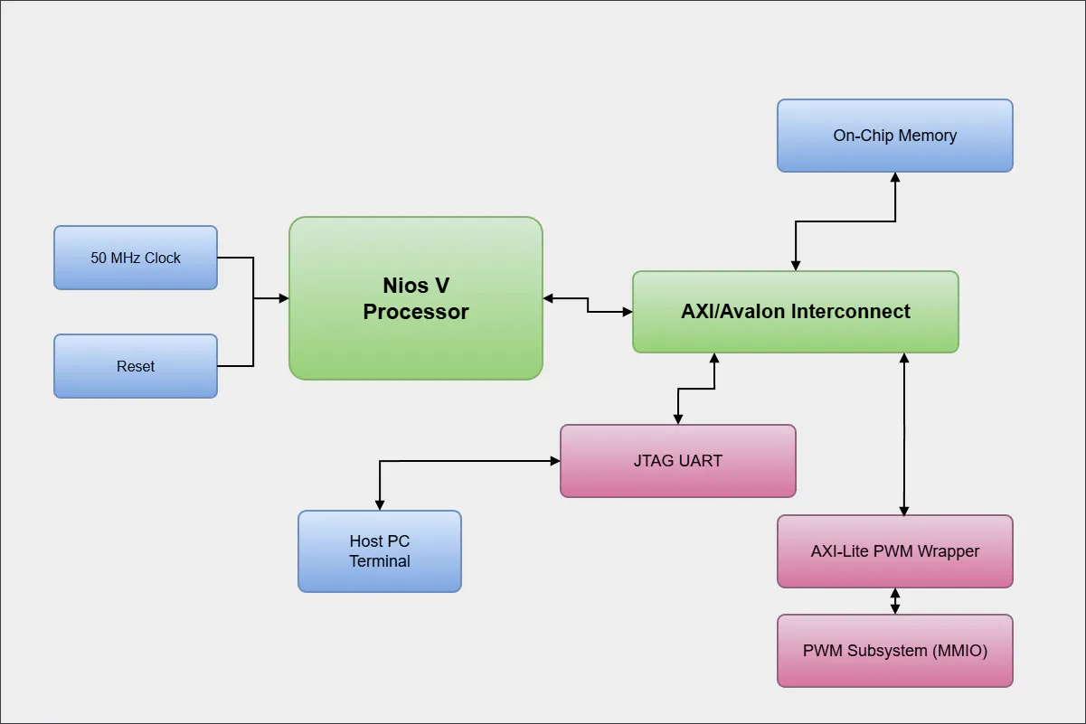
How it worksThe system includes:
- Nios V/m processor - Executes software
- On-chip memory - stores instructions and data
- JTAG UART - provides terminal output
- Clock/reset logic - drives the system
The processor fetches instructions from memory and sends outputs (or inputs) through the JTAG UART to the host PC.
Build Instructions*Note: a Free license to use NIOS V must be obtain at Altera's website.
It is free but you do have to create an account with them and "Self Service" your license. These steps are not covered here.
The Self-service link is here.
1. Install the Software and Tool ChainIt's important to note the location of installation, since we need to make sure a few directories are placed in the user's PATH
- Install Quartus Prime Lite 25.1
First download the Quartus Prime Lite Edition Installer (SFX) via this link:Quartus Lite download link
Notice the install location, in my case it's in the D: drive
Also, if you have more than one FPGA board (different FPGA family), select it here.
Also, install all the drivers as seen in the image
*Important: From other users, there might be missing features on the Ashling version included in this installer. So, don't select it here.
- Install Quartus Prime Pro Edition Programmer and Tools 25.1.1
In order to install the "pro" version of Ashling, the installer needs to detect an installation folder for Quartus Prime Pro Edition or it's Programmer and tools, so we can download the Quartus Prime Pro Edition Programmer and Tools 25.1.1 from here.
I also decided to install it on the D: drive as seen on the photo.
This installation will create the folder required to install the pro version of Ashling
- Install Ashling* RiscFree* IDE for Altera
Now we can download Ashling* RiscFree* IDE for Altera 25.1.1 "pro" version from here.
While installing, make sure to select the folder that was created for the "pro" version in my case it was:
D:\altera_pro\25.1.1As seen on this image
- Add the correct directories to the user's PATH
D:\altera_pro\25.1.1\riscfree\toolchain\riscv32-unknown-elf\bin
D:\altera_pro\25.1.1\riscfree\build_tools\cmake\bin
D:\altera_pro\25.1.1\riscfree\build_tools\bin
D:\altera_pro\25.1.1\riscfree\debugger\gdbserver-riscv
Here, I have accessed "environment variables" by going to "System Properties", then click on "Environment Variables...", and under "user variable for 'user'", I edited the "Path". As you can see in the rightmost window, I added the directory listed above.
2. Start a Quartus Project- File > New Project Wizard
- Start as an Empty Project
- Don't add any files and click on "Next>"
- On the "Family, Device & Board Settings" window, go to the Board type (this will depend on the board you are using and how comfortable you are with Quartus, if you got the same board as I do, just select the MAX 10 DE10-Lite, but it should work with any other Altera/Intel FPGA). I made sure that there was a check mark on "Create top-level design file." in order to speed up the definition of ports and pin assignments.
- On EDA Tool Settings leave as default and click "Finish"
- Just verify that the project was created successfully. On the left panel, on the Project Navigator, select "Files" from the drop-down menu. There should now a folder named "Files" with a verilog file: DE10_LITE_Golden_Top.v. Double-click it in order to see the top file, this is where all the pins on the board should show up.
- Click on the blue arrow to start compilation, it should finish all the compilation process (Analysis & Synthesis, Place & Route, Generate programming files, Timing Analysis) with no errors. Warnings are okay since nothing is driving the port pins.
- Open Platform Designer by going to Tools on the toolbar
- Create a new system and save it with a good name: e.g. niosv_system.qsys. I recommend creating a sub-folder named "pd" (platform designer) and store the system in this folder.
The following components will change as your needs change or as your project requires them. In this instance, I will add the minimum required components to run a stable system. By default, the "clk" component will show up, so you don't have to add that one manually.
In order to find the components quickly we will go to the left panel and look for the IP catalog. In this catalog there will be a "search" field. This is where we are going to look for our specific components.
Once we find the component we are looking for, we double-click it and the component will be auto added to the System and a configuration window will open up.
- Reset Bridge: the processor and most components need a stable reset signal to ensure no random bugs happen. Intel provides a Reset Bridge which takes a signal and synchronizes it to a clock edge. The only change here is to check the "Active low reset", this is because I will be using one if the "KEY" push-buttons on the board which normally output "high" and when they are pressed, they produces a "low" signal. I want the system to be reset when the push-button is sending a "low" signal. Once you let go of the button, they Reset Bridge will make sure that the rising edge of the push-button gets synchronized with the clock of the system. Once done, click "Finish".
- Nios V/m Microcontroller: Again, on the search bar enter "nios v" and double click on "Nios V/m Microcontroller IP" (the other two can work as well, but one is simpler, with less features (can be used to replace a FSM), and the other one can run a full OS. Altera describes them as: Compact Microcontroller, Microcontroller, and General-purpose processor, accordingly. All of them are designed for Altera FPGA devices and based on RISC-V specification, they do not include peripherals or the connection logic to external devices and they only include the circuitry required to implement the Nios V processor architecture and that's why we are doing this project to add circuitry to it.
In this case we will Enable Debug, for now, we will leave Traps, Exceptions, and Interrupts as it is, we'll come back to this once we add memory. For CPU architecture, we will leave Enable Pipelining in CPU enabled, it doesn't use many logic elements based on the FPGA on the DE10-Lite, if your FPGA has limited number of logic elements and the instructions-per-cycle is of no concern, disable pipelining.
- On-Chip Memory: Any processor needs memory to hold instructions and data. There are several options in an FPGA, I will just talk about a couple and implement the simplest one for this project, later we can move to a more advanced one.
First, FPGAs lose their configuration after power down. Most FPGA systems have an external flash memory where the FPGA circuitry configuration (bit-stream) is stored, this non-volatile memory will hold it's data even after powerloss. For the MAX10 FPGA on our board, this non-volatile memory is inside the FPGA chip.
But this flash memory, can't be used to run a processor, processors need fast memory such as RAM.
The DE10-Lite board has a RAM on it's pcb, it's SDRAM with 64MB of capacity! But it requires an SDRAM controller and other steps to use it, so it will be out of the scope of this project, even then, this memory is also volatile, so it will loose it's data and instructions on power down.
Now, the FPGA in our board has BRAM (block ram) that can be configured to used for the Nios V processor to run instructions from and store/read data. But this BRAM also erases after power down.
What we can do for now (for this project), is use the BRAM as instructions and data memory since there is a component that takes care of this for us.
After this, we can have Quartus to store the Nios V firmware in it's FPGA bit stream and it can get loaded in the the BRAM after power up along with the FPGA getting configured with our system. The biggest downside of using BRAM as the instruction and data memory is that it's limited and precious for other circuitry perhaps. But for now, we will use BRAM as the system memory.
Double-click on On-Chip memory (RAM or ROM) IP:
Choose Dual-Port access: In summary, it's faster, and it's complexity is taken care of automatically.
For memory size, let's choose 128 KB: in bytes it is 131072 (128 x 1024). It's enough to start up and use the HAL library from Intel.
Disable "Initialize memory content": We will be loading the firmware using JTAG through USB. Once the final firmware is ready to be loaded, then we can change this setting and point to the firmware binary file (.hex).
JTAG UART: We want to at least get the microcontroller to speak to use using the printf() function. Later we want to actually control devices using GPIO, but for now we need to do a sanity check on the system. Remember that the Nios V doesn't come with any peripherals, if we wanted to connect the fpga to a terminal through UART, we would have to find an implementation, either open source, license one or create one ourselves. Thankfully, Altera provides a UART module (component, implementation, core, however you want to call it), and it uses the the JTAG port through USB so your computer can see it as a COM port.
So look up the JTAG UART IP component on the search bar and double click it. Leave the default settings, it's good the way it is.
There are two signals that are exported, meaning, that this signals are visible to us and we can connect signals. These two signals are on the the clk component and are: clk_in and clk_in_reset; we are not connecting anything to these two signal with Platform Designer.
All the modules need a clock to work, so let's connect the clock output signal to all the other modules/components/IPs. You create the interconnection by clicking on the vertex (the little ball that intersects two lines).
As more signals get connected, the errors in read will start disappearing.
Also, all the modules need a reset signal, but this reset signal should be synchronized. This is done by the reset_bridge component. The reset_bridge requires a raw reset signal to condition it and create a synchronized signal. So first, let's connect the clk_0 module's clk_reset signal to the in_reset signal of the reset_bridge.
All the other modules require a reset signal, now we can provide them one that has already been conditioned. Connect the out_reset signal from the reset_bridge into all the reset inputs from all the other modules (except clk_0 module). *Notice that the onchip_memory has two reset inputs (reset1 and reset2), one per port, connect the reset signal to both ports.
Finally, we have to connect the system memory (and jtag_uart) into the processor. The processor has two ports, the data port and the instructions port (data_manager and instruction_manager). Since we split the On-Chip memory to have dual-ports, we can connect each side to their own ports, (this way, we can fetch instructions and access/store data in the same cycle if necessary, which is internally done by the processor). The port order doesn't matter, it's all taken care by the BSP tools. Connect the signals as shown on the picture below.
We also connect jtag_uart's avalon_jtag_slave port to the data_manager port of the niosv_m module
and finally, connect the jtag_uart's irq port to the niosv's platform_irq_rx port.
Woah!! errors popped up!!!
Let's fix them in the next part.
6. Assign AddressesThe way modern processors deal with I/O and other system modules is to treat them as if they were memory. That way, if you want to access a module/peripheral, you just need to talk to it as if it was data by writing and reading to its address, data address. The processor doesn't know whether it's actually accessing data, or reaching out to a piece of hardware.
Just like in mailing system, there can't be two addresses that are the same, the same is true with peripherals in a computer system. The errors above is pretty much complaining that there are modules that have the same memory addresses. You can either choose the addresses and ranges manually or you can have Platform Designer to solve this issue automatically. By going to System>Assign Base Addresses
We need to go back and edit the intel_niosv_m_o (right click and edit) component now that we have integrated the memory into this system. Under Traps, Exceptions, and Interrupts, let's choose the correct Reset Agent to: onchip_memory2_0.s1 (or s2 if you connected second channel to the instruction port).
The system should have all the minimum requirements to run a microcontroller and be able to debug it by using the printf() function. Let's make sure we save the changes to this system by the keyboard shortcut ctrl+s or going to File>Save; A dialog will say if it was successful to save the changes.
On the bottom right of the page, there is a button called "Generate HDL..." let's press this button so Platform Designer can generate the hardware description files and then we can instantiate the whole system.
Notice the Output Directory, in my case it's: D:/fpga_projects/niosv_sopc/pd/niosv_systemWe need to open this directory in order to open the file named: niosv_system_inst.v
To integrate our niosv_system into our fpga project, first we need to add the.quip file into our project manually. Go to the Project menu and click on Add/Remove Files in Project... Then click on the button with the 3 dots net to the File name: field. Then navigate to the folder "pd" we created earlier, then "niosv_system", then "synthesis" and open "niosv_system.qip".
Then, Apply> OK
Now, we have to open up the niosv_system_inst.v and copy paste the instantiation layout. It is in the directory noted earlier: niosv_sopc/pd/nios_system/niosv_system_inst.v
We will paste this piece of code into the the DE10_LITE_Golden_top.v that we opened at the beginning of the whole project. We can paste it anywhere after the port declaration and before "endmodule" but for file that was provided in Quartus there is section where it will make sense. Which is under a commented section as: structural coding
After this we connect the DE10-lites clock to the clock input of the niosv_system and we connect the board's KEY[0] to the reset input of the niosv_system.
Now we start the compilation one more time and everything should work fine.
8. Compile & Program
Now that we have verified that the SOPC system interconnects and compiles correctly, we have to create the source files and folder for the software side of the system.
- We need to download the compiled hardware bitstream into the DE10-Lite Board
Let's open up the Programmer and download the bitstream to the board:
Create Folders
We do this by creating a specific board structure and creating source files. We will create a folder named sw (this folder will hold all the software files and folders)
Inside the sw folder, we will create two folders: app and bsp
We will store the source files in the app folder. Let's create a main.c file in this folder and write a "Hello world! C code
#include <stdio.h>
#include <stdint.h>

int main(void)
{
    printf("Hello World");


	while(1)
	{
	}

	return 0;
}This step is the software-side hardware abstraction layer that bridges the compiled hardware system with the C application. It pretty much defines memory regions and setup startup code and gives entry to the main() function. Platform designer saves the SOPC settings in a.sopcinfo file and Altera provides software to generate the necessary files and libraries to interact with our system.
For that we need to open up the CLI application: Nios V Command Shell that gets install by during Quartus installation process.
After opening the Nios V Command Shell we need to make sure we change directory to the project root directory.
niosv-bsp --create --sopcinfo=..\pd\niosv_system.sopcinfo --type=hal bsp\settings.bsprun this command: it will populate the BSP folder we created. Make sure to put the correct directory for niosv_system.sopcinfo (or whatever you named it).
- Setup directories
The following command will setup where the application will live and tells it where the BSP is located (the system.h files and other drivers). It will also generate the "app\CMakeLists.txt" file.
niosv-app --app-dir=app --bsp-dir=bsp --srcs=app- Build Application
The we need to use CMake to configure our project, it will read the CMakeLists.txt file, generate a Makefile-based build system and place all build artifacts in the build/ directory.
First, we need to move to the app/ folder and the run:
cmake -B build -S . -G "Unix Makefiles"Once everything is setup, then we can start building the binary files (.hex,.elf, etc).
by using the following command:
cmake --build build- Download Application to memory
If everything that has compiled correctly and programming the FPGA board with the bitstream then we are ready to download the Nios V executable file into the system.
niosv-download -g build/app.elf- If everything has been done correctly, we can check if the Nios V system is outputting the "Hello World" string by looking into the JTAG UART Terminal by using the following command.
juart-terminalTo exit the terminal, press ctrl-c on the keyboard
Source CodeNow that the project worked, if there is a change in the project (doing modification in Platform Designer), the whole building process has to be redone.
But if it's just the application code that is changing, only recompilation is needed (cmake --build build).
This time I updated the code with this sample program to test simple C constructs and testing the Altera HAL function usleep().
#include <stdio.h>
#include <stdint.h>
#include <unistd.h>   // usleep()

int main(void)
{
    printf("=== Nios V Basic Test Start ===\n");

    // -------------------------------------------------
    // 1. Variable test
    // -------------------------------------------------
    int a = 5;
    int b = 10;
    int sum = a + b;

    printf("Variable test: %d + %d = %d\n", a, b, sum);

    // -------------------------------------------------
    // 2. Loop test (for loop)
    // -------------------------------------------------
    printf("\nFor loop test:\n");

    for (int i = 0; i < 5; i++) {
        printf("  i = %d\n", i);
        usleep(200000); // 200 ms delay
    }

    // -------------------------------------------------
    // 3. While loop test
    // -------------------------------------------------
    printf("\nWhile loop test:\n");

    int counter = 3;
    while (counter > 0) {
        printf("  counter = %d\n", counter);
        counter--;
        usleep(300000); // 300 ms delay
    }

    // -------------------------------------------------
    // 4. Timing / delay test
    // -------------------------------------------------
    printf("\nDelay test (1 second total):\n");

    for (int i = 0; i < 5; i++) {
        printf("  tick %d\n", i);
        usleep(200000); // 5 × 200 ms = 1 second
    }

    // -------------------------------------------------
    // 5. Infinite loop (heartbeat)
    // -------------------------------------------------
    printf("\nEntering main loop...\n");

    uint32_t heartbeat = 0;

    while (1) {
        printf("Heartbeat: %lu\n", heartbeat++);
        usleep(500000); // 500 ms

        // simple rollover test
        if (heartbeat == 10) {
            printf("Resetting heartbeat...\n");
            heartbeat = 0;
        }
    }

    return 0;
}
Just run the cmake --build build command
and download again using niosv-download -g build/app.elf
and check again in the terminal by using juart-terminal
- Memory Initialization
- incorrect SOPCINFO Path
- RiscFree Tools Not Detected
- CMake Generator Mismatch
- Windows Path Issues in Debugger
- Missing GDB Server
This project is available in two repository forms, depending on the level of depth you want to explore.
Minimal Bring-Up (Smoke Test)https://github.com/eftorres-embedded/fpga-pwm-axi-niosv-smoke
This repository is a clean, minimal implementation focused on validating the full toolchain and hardware flow:
- Nios V bring-up
- On-chip memory + JTAG UART
- Basic MMIO interaction
- PWM control from software
It is intended for readers who want a low-complexity, reproducible starting point.
Full Modular Systemhttps://github.com/eftorres-embedded/fpga-modular-control-system
This repository expands the design into a scalable FPGA system architecture, including:
- multiple peripherals (PWM, SPI, UART, LCD)
- reusable AXI4-Lite register layers
- separation between datapath, control, and bus interfaces
It is intended for readers who want to explore a more complete SoC-style design and follow the project as it evolves.
RecommendationIf you are new to this flow, start with the smoke test repository.
If you are interested in system architecture and reusable design patterns, follow the modular control system repository.
In this article, the minimal bring-up repository is used as the reference implementation.


Comments