
Hardware components | ||||||
 |
| × | 1 | |||
|
| × | 1 | |||
 |
| × | 1 | |||
| × | 1 | ||||
| × | 1 | ||||
| × | 1 | ||||
Software apps and online services | ||||||
| ||||||
In this project we shall build an FPGA imaging platform from scratch. The goal is to interface a VGA resolution CMOS camera with the MiniZed Development board and output the acquired live video feed to a VGA monitor. The complete imaging pipeline will be implemented in the PL (Programmable Logic) section of the SoC.
The image above shows the live QVGA video feed from the OV7670 CMOS camera being streamed to the VGA screen.
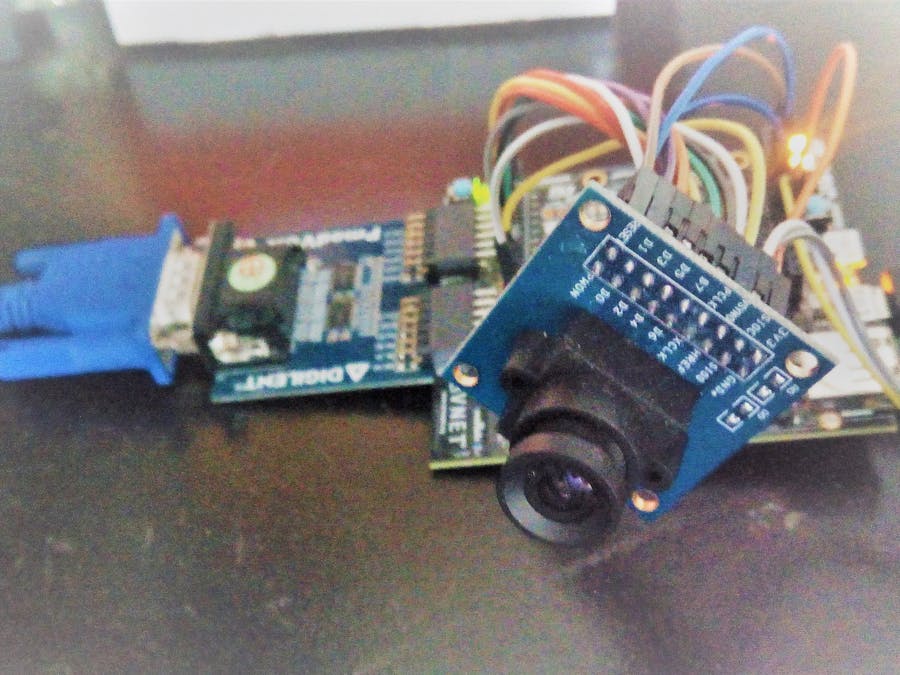
The hardware for this project consists of an OV7670 camera, a ZYNQ FPGA SoC MiniZed Development board, a VGA DAC and a generic VGA monitor.
The MiniZed contains an Arduino connector and 2 PMOD connectors. A VGA PMOD will be connected to the two PMOD's while the OV7670 camera will be connected to the Arduino connector via male to female fly-wires. The pins will be configured to operate at 2.5V logic levels so that the electrical interface is compatible.
CameraThe OV7670 is a CMOS parallel camera with VGA resolution from Omnivison. The camera can operate from 1.7 to 3V. The camera interface consists of a parallel 8 bit bus, synchronization signals VSYNC and HSYNC, pixel clock, master clock, and reset and power down signals.
The module for the frame capture was borrowed by Mike Field( Hamsterworks).
The camera interfacing code consists of two main modules. The input capture image and the camera configuration image. The input capture code is responsible of transmitting the pixels to the frame buffer. This module decodes the pixels coming from the camera.
Each pixel is packed into 2 consecutive bytes. The Input capture modules converts this to RGB444. This is done to save space since the VGA interface uses a RGB444 interface.
The camera supports multiple pixel image formats however the one selected in this application is RGB565 meaning Red, Green and Blue gets 5, 6, and 5 pixels each respectively.
The camera is configured via SCCB (Serial Camera Communication Bus). This is mostly compatible with I2C.
VGATo interface the Minized with a VGA monitor we have to use a current DAC (digital to analog converter). The Digilent VGA PMOD is an R2R DAC composed of two high-speed buffers and an R2R digital to analog converter. It has 12 bit resolution which means 4 bits for each color (red, green and blue), RGB444.
The VGA IP module takes the 12 bit pixels and generates the timing synchronization circuits used to interface with the display.
Putting the hardware together is relatively simple. Once the VGA DAC is plugged in the PMOD the camera has to be connected to the Arduino connector.
Video MemoryThe main issue one encounters when implementing the camera on the MiniZed is the limited amount of BRAM the MiniZed has. The ZYNQ XC7007 does not have enough memory to store a complete VGA frame.
The workaround this is to store a QVGA image frame and program the VGA IP to output a full VGA frame with the QVGA image at the corner of the screen.
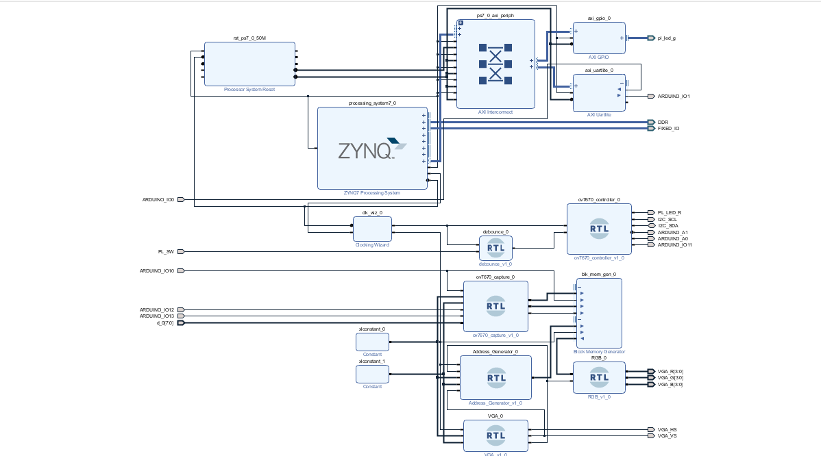
Top Level DesignThe schematic of the design are shown below. The top level design consists of the ZYNQ-7000 PS section and the programmable logic blocks implemented in the PL section. Since all the logic is implemented in the PL this is a streaming architecture. All the data coming from the camera are streamed directly to the VGA screen.
The PL logic blocks are as follows:
- OV7670 input capture Module
- OV7670 Camera configuration module
- BRAM for storing a full QVGA frame
- ZYNQ-7000
- Clocking wizard
- Address Generator
- VGA IP core
The OV7670 Configuration module implements the I2C protocol in HDL and the commands are read from a LUT (Look up table).
A dual port BRAM is used to store and read data from. The pixel clock sources PortA clock of the dual port BRAM. Port A of the BRAM is used to store the image from the camera. Port B of the BRAM is interfaced with an address generator which reads the data and pipes the pixels to a VGA IP module.
The clocking wizard generates a 25.175 MHz clock which clocks the VGA module. This is the required clock for a resolution of 640x480. The second clock of 50MHz is used to clock the configuration module.
After the synthesis and implementation stages a bitstream will be generated. Next steps are to launch the SDK, create a Hello world project, transfer the bitstream and run the app.
The image below shows the complete hardware platform kludged together. It's important to keep the length of the wires short to avoid signal integrity issues.
One important note is the configuration of the camera with the proper settings. Below one can see the trippy effect one gets when configuring the camera to output in YCbCr image format. As mentioned the correct format for the architecture above is RGB565.
The.tcl file and the code have been uploaded on Github. To recreate the project make a new project in Vivado. Select the MiniZed platform and switch to the current directory. Then add the VHDL source files to the project. Finally to create the project issue:
source minizedCamera.tcl
This will recreate the complete project. This will result in a continuous video feed being transferred to the VGA screen at 30 frames per second. That pretty much concludes the project.
SummaryThis project showed how to interface a CMOS parallel camera with an FPGA SoC. The QVGA camera frames are streamed to a VGA monitor at 30 frames per second thereby implementing a complete imaging platform on the MiniZed SoC.
----------------------------------------------------------------------------------
-- Engineer: Mike Field <hamster@snap.net.nz>
--
-- Description: Captures the pixels coming from the OV7670 camera and
--              Stores them in block RAM
--
-- The length of href last controls how often pixels are captive - (2 downto 0) stores
-- one pixel every 4 cycles.
--
-- "line" is used to control how often data is captured. In this case every forth
-- line
----------------------------------------------------------------------------------
library IEEE;
use IEEE.STD_LOGIC_1164.ALL;
use IEEE.NUMERIC_STD.ALL;

entity ov7670_capture is
    Port ( pclk  : in   STD_LOGIC;
           rez_160x120 : IN std_logic;
           rez_320x240 : IN std_logic;
           vsync : in   STD_LOGIC;
           href  : in   STD_LOGIC;
           d     : in   STD_LOGIC_VECTOR (7 downto 0);
           addr  : out  STD_LOGIC_VECTOR (17 downto 0);
           dout  : out  STD_LOGIC_VECTOR (11 downto 0);
           we    : out  STD_LOGIC);
end ov7670_capture;

architecture Behavioral of ov7670_capture is
   signal d_latch      : std_logic_vector(15 downto 0) := (others => '0');
   signal address      : STD_LOGIC_VECTOR(17 downto 0) := (others => '0');
   signal line         : std_logic_vector(1 downto 0)  := (others => '0');
   signal href_last    : std_logic_vector(6 downto 0)  := (others => '0');
   signal we_reg       : std_logic := '0';
   signal href_hold    : std_logic := '0';
   signal latched_vsync : STD_LOGIC := '0';
   signal latched_href  : STD_LOGIC := '0';
   signal latched_d     : STD_LOGIC_VECTOR (7 downto 0) := (others => '0');
begin
   addr <= address;
   we <= we_reg;
   dout    <= d_latch(15 downto 12) & d_latch(10 downto 7) & d_latch(4 downto 1);

capture_process: process(pclk)
   begin
      if falling_edge(pclk) then
         if we_reg = '1' then
            address <= std_logic_vector(unsigned(address)+1);
         end if;

         -- This is a bit tricky href starts a pixel transfer that takes 3 cycles
         --        Input   | state after clock tick
         --         href   | wr_hold    d_latch           dout                we address  address_next
         -- cycle -1  x    |    xx      xxxxxxxxxxxxxxxx  xxxxxxxxxxxx  x   xxxx     xxxx
         -- cycle 0   1    |    x1      xxxxxxxxRRRRRGGG  xxxxxxxxxxxx  x   xxxx     addr
         -- cycle 1   0    |    10      RRRRRGGGGGGBBBBB  xxxxxxxxxxxx  x   addr     addr
         -- cycle 2   x    |    0x      GGGBBBBBxxxxxxxx  RRRRGGGGBBBB  1   addr     addr+1

         -- detect the rising edge on href - the start of the scan line
         if href_hold = '0' and latched_href = '1' then
            case line is
               when "00"   => line <= "01";
               when "01"   => line <= "10";
               when "10"   => line <= "11";
               when others => line <= "00";
            end case;
         end if;
         href_hold <= latched_href;

         -- capturing the data from the camera, 12-bit RGB
         if latched_href = '1' then
            d_latch <= d_latch( 7 downto 0) & latched_d;
         end if;
         we_reg  <= '0';

         -- Is a new screen about to start (i.e. we have to restart capturing
         if latched_vsync = '1' then
            address      <= (others => '0');
            href_last    <= (others => '0');
            line         <= (others => '0');
         else
            -- If not, set the write enable whenever we need to capture a pixel
            if (rez_160x120 = '1' and href_last(6) = '1') or
               (rez_320x240 = '1' and href_last(2) = '1') or
               (rez_160x120 = '0' and rez_320x240  = '0' and href_last(0) = '1') then

               if rez_160x120 = '1' then
                  if line = "10" then
                     we_reg <= '1';
                   end if;
               elsif rez_320x240 = '1' then
                  if line(1) = '1' then
                     we_reg <= '1';
                   end if;
               else
                   we_reg <= '1';
               end if;
               href_last <= (others => '0');
            else
               href_last <= href_last(href_last'high-1 downto 0) & latched_href;
            end if;
         end if;
      end if;
      if falling_edge(pclk) then
         latched_d     <= d;
         latched_href  <= href;
         latched_vsync <= vsync;
      end if;
   end process;
end Behavioral;
----------------------------------------------------------------------------------
-- Engineer: Mike Field <hamster@snap.net.nz>
--
-- Description: Controller for the OV760 camera - transferes registers to the
--              camera over an I2C like bus
----------------------------------------------------------------------------------
library IEEE;
use IEEE.STD_LOGIC_1164.ALL;
use IEEE.NUMERIC_STD.ALL;

entity ov7670_controller is
    Port ( clk   : in    STD_LOGIC;
			  resend :in    STD_LOGIC;
			  config_finished : out std_logic;
           sioc  : out   STD_LOGIC;
           siod  : inout STD_LOGIC;
           reset : out   STD_LOGIC;
           pwdn  : out   STD_LOGIC;
			  xclk  : out   STD_LOGIC
);
end ov7670_controller;

architecture Behavioral of ov7670_controller is
	COMPONENT i3c2 GENERIC (
		clk_divide  : std_logic_vector(7 downto 0)
   );
	PORT(
		clk : IN std_logic;
		inst_data : IN std_logic_vector(8 downto 0);
		inputs : IN std_logic_vector(15 downto 0);
		i2c_sda : INOUT std_logic;
		inst_address : OUT std_logic_vector(9 downto 0);
		i2c_scl : OUT std_logic;
		outputs : OUT std_logic_vector(15 downto 0);
		reg_addr : OUT std_logic_vector(4 downto 0);
		reg_data : OUT std_logic_vector(7 downto 0);
		reg_write : OUT std_logic;
		error : OUT std_logic
		);
	END COMPONENT;

   signal inputs  : std_logic_vector(15 downto 0);
   signal outputs : std_logic_vector(15 downto 0);
   signal data    : std_logic_vector( 8 downto 0);
   signal address : std_logic_vector( 9 downto 0);
   signal sys_clk : std_logic;
begin
   inputs(0) <= resend;
   config_finished <= outputs(0);

	Inst_i3c2: i3c2 GENERIC MAP(
      clk_divide => std_logic_vector(to_unsigned(125,8))
   ) PORT MAP(
		clk => clk,
		inst_address => address ,
		inst_data => data,
		i2c_scl => sioc,
		i2c_sda => siod,
		inputs => inputs,
		outputs => outputs,
		reg_addr => open,
		reg_data => open,
		reg_write => open,
		error => open
	);

	reset <= '1'; 						-- Normal mode
	pwdn  <= '0'; 						-- Power device up
	xclk  <= sys_clk;

	process(clk)
	begin
		if rising_edge(clk) then
			sys_clk <= not sys_clk;

         case address is
           when "0000000000" => data <= "011100100";
           when "0000000001" => data <= "101000010";
           when "0000000010" => data <= "100010010";
           when "0000000011" => data <= "110000000";
           when "0000000100" => data <= "011111111";
           when "0000000101" => data <= "011101001";
           when "0000000110" => data <= "101000010";
           when "0000000111" => data <= "100010010";
           when "0000001000" => data <= "100000100";
           when "0000001001" => data <= "011111111";
           when "0000001010" => data <= "101000010";
           when "0000001011" => data <= "100010001";
           when "0000001100" => data <= "100000000";
           when "0000001101" => data <= "011111111";
           when "0000001110" => data <= "101000010";
           when "0000001111" => data <= "100001100";
           when "0000010000" => data <= "100000000";
           when "0000010001" => data <= "011111111";
           when "0000010010" => data <= "101000010";
           when "0000010011" => data <= "100111110";
           when "0000010100" => data <= "100000000";
           when "0000010101" => data <= "011111111";
           when "0000010110" => data <= "101000010";
           when "0000010111" => data <= "110001100";
           when "0000011000" => data <= "100000000";
           when "0000011001" => data <= "011111111";
           when "0000011010" => data <= "101000010";
           when "0000011011" => data <= "100000100";
           when "0000011100" => data <= "100000000";
           when "0000011101" => data <= "011111111";
           when "0000011110" => data <= "101000010";
           when "0000011111" => data <= "101000000";
           when "0000100000" => data <= "100010000";
           when "0000100001" => data <= "011111111";
           when "0000100010" => data <= "101000010";
           when "0000100011" => data <= "100111010";
           when "0000100100" => data <= "100000100";
           when "0000100101" => data <= "011111111";
           when "0000100110" => data <= "101000010";
           when "0000100111" => data <= "100010100";
           when "0000101000" => data <= "100111000";
           when "0000101001" => data <= "011111111";
           when "0000101010" => data <= "101000010";
           when "0000101011" => data <= "101001111";
           when "0000101100" => data <= "101000000";
           when "0000101101" => data <= "011111111";
           when "0000101110" => data <= "101000010";
           when "0000101111" => data <= "101010000";
           when "0000110000" => data <= "100110100";
           when "0000110001" => data <= "011111111";
           when "0000110010" => data <= "101000010";
           when "0000110011" => data <= "101010001";
           when "0000110100" => data <= "100001100";
           when "0000110101" => data <= "011111111";
           when "0000110110" => data <= "101000010";
           when "0000110111" => data <= "101010010";
           when "0000111000" => data <= "100010111";
           when "0000111001" => data <= "011111111";
           when "0000111010" => data <= "101000010";
           when "0000111011" => data <= "101010011";
           when "0000111100" => data <= "100101001";
           when "0000111101" => data <= "011111111";
           when "0000111110" => data <= "101000010";
           when "0000111111" => data <= "101010100";
           when "0001000000" => data <= "101000000";
           when "0001000001" => data <= "011111111";
           when "0001000010" => data <= "101000010";
           when "0001000011" => data <= "101011000";
           when "0001000100" => data <= "100011110";
           when "0001000101" => data <= "011111111";
           when "0001000110" => data <= "101000010";
           when "0001000111" => data <= "100111101";
           when "0001001000" => data <= "111000000";
           when "0001001001" => data <= "011111111";
           when "0001001010" => data <= "101000010";
           when "0001001011" => data <= "100010001";
           when "0001001100" => data <= "100000000";
           when "0001001101" => data <= "011111111";
           when "0001001110" => data <= "101000010";
           when "0001001111" => data <= "100010111";
           when "0001010000" => data <= "100010001";
           when "0001010001" => data <= "011111111";
           when "0001010010" => data <= "101000010";
           when "0001010011" => data <= "100011000";
           when "0001010100" => data <= "101100001";
           when "0001010101" => data <= "011111111";
           when "0001010110" => data <= "101000010";
           when "0001010111" => data <= "100110010";
           when "0001011000" => data <= "110100100";
           when "0001011001" => data <= "011111111";
           when "0001011010" => data <= "101000010";
           when "0001011011" => data <= "100011001";
           when "0001011100" => data <= "100000011";
           when "0001011101" => data <= "011111111";
           when "0001011110" => data <= "101000010";
           when "0001011111" => data <= "100011010";
           when "0001100000" => data <= "101111011";
           when "0001100001" => data <= "011111111";
           when "0001100010" => data <= "101000010";
           when "0001100011" => data <= "100000011";
           when "0001100100" => data <= "100001010";
           when "0001100101" => data <= "011111111";
           when "0001100110" => data <= "101000010";
           when "0001100111" => data <= "100001110";
           when "0001101000" => data <= "101100001";
           when "0001101001" => data <= "011111111";
           when "0001101010" => data <= "101000010";
           when "0001101011" => data <= "100001111";
           when "0001101100" => data <= "101001011";
           when "0001101101" => data <= "011111111";
           when "0001101110" => data <= "101000010";
           when "0001101111" => data <= "100010110";
           when "0001110000" => data <= "100000010";
           when "0001110001" => data <= "011111111";
           when "0001110010" => data <= "101000010";
           when "0001110011" => data <= "100011110";
           when "0001110100" => data <= "100110111";
           when "0001110101" => data <= "011111111";
           when "0001110110" => data <= "101000010";
           when "0001110111" => data <= "100100001";
           when "0001111000" => data <= "100000010";
           when "0001111001" => data <= "011111111";
           when "0001111010" => data <= "101000010";
           when "0001111011" => data <= "100100010";
           when "0001111100" => data <= "110010001";
           when "0001111101" => data <= "011111111";
           when "0001111110" => data <= "101000010";
           when "0001111111" => data <= "100101001";
           when "0010000000" => data <= "100000111";
           when "0010000001" => data <= "011111111";
           when "0010000010" => data <= "101000010";
           when "0010000011" => data <= "100110011";
           when "0010000100" => data <= "100001011";
           when "0010000101" => data <= "011111111";
           when "0010000110" => data <= "101000010";
           when "0010000111" => data <= "100110101";
           when "0010001000" => data <= "100001011";
           when "0010001001" => data <= "011111111";
           when "0010001010" => data <= "101000010";
           when "0010001011" => data <= "100110111";
           when "0010001100" => data <= "100011101";
           when "0010001101" => data <= "011111111";
           when "0010001110" => data <= "101000010";
           when "0010001111" => data <= "100111000";
           when "0010010000" => data <= "101110001";
           when "0010010001" => data <= "011111111";
           when "0010010010" => data <= "101000010";
           when "0010010011" => data <= "100111001";
           when "0010010100" => data <= "100101010";
           when "0010010101" => data <= "011111111";
           when "0010010110" => data <= "101000010";
           when "0010010111" => data <= "100111100";
           when "0010011000" => data <= "101111000";
           when "0010011001" => data <= "011111111";
           when "0010011010" => data <= "101000010";
           when "0010011011" => data <= "101001101";
           when "0010011100" => data <= "101000000";
           when "0010011101" => data <= "011111111";
           when "0010011110" => data <= "101000010";
           when "0010011111" => data <= "101001110";
           when "0010100000" => data <= "100100000";
           when "0010100001" => data <= "011111111";
           when "0010100010" => data <= "101000010";
           when "0010100011" => data <= "101101001";
           when "0010100100" => data <= "100000000";
           when "0010100101" => data <= "011111111";
           when "0010100110" => data <= "101000010";
           when "0010100111" => data <= "101101011";
           when "0010101000" => data <= "101001010";
           when "0010101001" => data <= "011111111";
           when "0010101010" => data <= "101000010";
           when "0010101011" => data <= "101110100";
           when "0010101100" => data <= "100010000";
           when "0010101101" => data <= "011111111";
           when "0010101110" => data <= "101000010";
           when "0010101111" => data <= "110001101";
           when "0010110000" => data <= "101001111";
           when "0010110001" => data <= "011111111";
           when "0010110010" => data <= "101000010";
           when "0010110011" => data <= "110001110";
           when "0010110100" => data <= "100000000";
           when "0010110101" => data <= "011111111";
           when "0010110110" => data <= "101000010";
           when "0010110111" => data <= "110001111";
           when "0010111000" => data <= "100000000";
           when "0010111001" => data <= "011111111";
           when "0010111010" => data <= "101000010";
           when "0010111011" => data <= "110010000";
           when "0010111100" => data <= "100000000";
           when "0010111101" => data <= "011111111";
           when "0010111110" => data <= "101000010";
           when "0010111111" => data <= "110010001";
           when "0011000000" => data <= "100000000";
           when "0011000001" => data <= "011111111";
           when "0011000010" => data <= "101000010";
           when "0011000011" => data <= "110010110";
           when "0011000100" => data <= "100000000";
           when "0011000101" => data <= "011111111";
           when "0011000110" => data <= "101000010";
           when "0011000111" => data <= "110011010";
           when "0011001000" => data <= "100000000";
           when "0011001001" => data <= "011111111";
           when "0011001010" => data <= "101000010";
           when "0011001011" => data <= "110110000";
           when "0011001100" => data <= "110000100";
           when "0011001101" => data <= "011111111";
           when "0011001110" => data <= "101000010";
           when "0011001111" => data <= "110110001";
           when "0011010000" => data <= "100001100";
           when "0011010001" => data <= "011111111";
           when "0011010010" => data <= "101000010";
           when "0011010011" => data <= "110110010";
           when "0011010100" => data <= "100001110";
           when "0011010101" => data <= "011111111";
           when "0011010110" => data <= "101000010";
           when "0011010111" => data <= "110110011";
           when "0011011000" => data <= "110000010";
           when "0011011001" => data <= "011111111";
           when "0011011010" => data <= "101000010";
           when "0011011011" => data <= "110111000";
           when "0011011100" => data <= "100001010";
           when "0011011101" => data <= "011111111";
           when "0011011110" => data <= "011111110";
           when "0011011111" => data <= "011111110";
           when "0011100000" => data <= "010000000";
           when "0011100001" => data <= "000000000";
           when "0011100010" => data <= "000011100";
           when others => data <= (others =>'0');
        end case;
		end if;
	end process;
end Behavioral;
----------------------------------------------------------------------------------
-- Engineer: Mike Field <hamster@snap.net.nz>
--
-- Create Date:    21:30:20 05/25/2013
-- Design Name:    i3c2 - Intelligent I2C Controller
-- Module Name:    i3c2 - Behavioral
-- Description:    The main CPU/logic
--
-- Revision:
-- Revision 0.01 - File Created
-- Additional Comments:
--
----------------------------------------------------------------------------------
library IEEE;
use IEEE.STD_LOGIC_1164.ALL;
use IEEE.NUMERIC_STD.ALL;

entity i3c2 is
   Generic( clk_divide : STD_LOGIC_VECTOR (7 downto 0));

    Port ( clk : in  STD_LOGIC;
           inst_address : out  STD_LOGIC_VECTOR (9 downto 0);
           inst_data : in  STD_LOGIC_VECTOR (8 downto 0);
           i2c_scl : out  STD_LOGIC;
           i2c_sda : inout  STD_LOGIC;
           inputs : in  STD_LOGIC_VECTOR (15 downto 0);
           outputs : out  STD_LOGIC_VECTOR (15 downto 0) := (others => '0');
           reg_addr : out  STD_LOGIC_VECTOR (4 downto 0);
           reg_data : out  STD_LOGIC_VECTOR (7 downto 0);
           reg_write : out  STD_LOGIC;
           error : out STD_LOGIC);
end i3c2;

architecture Behavioral of i3c2 is

   constant STATE_RUN       : std_logic_vector(3 downto 0) := "0000";
   constant STATE_DELAY     : std_logic_vector(3 downto 0) := "0001";
   constant STATE_I2C_START : std_logic_vector(3 downto 0) := "0010";
   constant STATE_I2C_BITS  : std_logic_vector(3 downto 0) := "0011";
   constant STATE_I2C_STOP  : std_logic_vector(3 downto 0) := "0100";
   signal   state           : std_logic_vector(3 downto 0) := STATE_RUN;

   constant OPCODE_JUMP      : std_logic_vector( 3 downto 0) := "0000";
   constant OPCODE_SKIPSET   : std_logic_vector( 3 downto 0) := "0001";
   constant OPCODE_SKIPCLEAR : std_logic_vector( 3 downto 0) := "0010";
   constant OPCODE_SET       : std_logic_vector( 3 downto 0) := "0011";
   constant OPCODE_CLEAR     : std_logic_vector( 3 downto 0) := "0100";
   constant OPCODE_I2C_READ  : std_logic_vector( 3 downto 0) := "0101";
   constant OPCODE_DELAY     : std_logic_vector( 3 downto 0) := "0110";
   constant OPCODE_SKIPACK   : std_logic_vector( 3 downto 0) := "0111";
   constant OPCODE_SKIPNACK  : std_logic_vector( 3 downto 0) := "1000";
   constant OPCODE_NOP       : std_logic_vector( 3 downto 0) := "1001";
   constant OPCODE_I2C_STOP  : std_logic_vector( 3 downto 0) := "1010";
   constant OPCODE_I2C_WRITE : std_logic_vector( 3 downto 0) := "1011";
   constant OPCODE_WRITELOW  : std_logic_vector( 3 downto 0) := "1100";
   constant OPCODE_WRITEHI   : std_logic_vector( 3 downto 0) := "1101";
   constant OPCODE_UNKNOWN   : std_logic_vector( 3 downto 0) := "1110";
   signal   opcode           : std_logic_vector( 3 downto 0);


   signal ack_flag      : std_logic := '0';
   signal skip          : std_logic := '1';   -- IGNORE THE FIRST INSTRUCTION

   -- I2C status
   signal i2c_doing_read : std_logic := '0';
   signal i2c_started    : std_logic := '0';
   signal i2c_bits_left  : unsigned(3 downto 0);

   -- counters
   signal pcnext         : unsigned(9 downto 0) := (others => '0');
   signal delay         : unsigned(15 downto 0);
   signal bitcount      : unsigned( 7 downto 0);

   -- Input/output data
   signal i2c_data  : std_logic_vector( 8 downto 0);

begin

-- |Opcode   | Instruction | Action
-- +---------+-------------+----------------------------------------
-- |00nnnnnnn| JUMP m      | Set PC to m (n = m/8)
-- |01000nnnn| SKIPCLEAR n | Skip if input n clear
-- |01001nnnn| SKIPSET n   | skip if input n set
-- |01010nnnn| CLEAR n     | Clear output n
-- |01011nnnn| SET n       | Set output n
-- |0110nnnnn| READ n      | Read to register n
-- |01110nnnn| DELAY m     | Delay m clock cycles (n = log2(m))
-- |011110000| SKIPNACK    | Skip if NACK is set
-- |011110001| SKIPACK     | Skip if ACK is set
-- |011110010| WRITELOW    | Write inputs 7 downto 0 to the I2C bus
-- |011110011| WRITEHI     | Write inputs 15 downto 8 to the I2C bus
-- |011110100| USER0       | User defined
-- |.........|             |
-- |011111110| USER9       | User defined
-- |011111111| STOP        | Send Stop on i2C bus
-- |1nnnnnnnn| WRITE n     | Output n on I2C bus

   opcode <= OPCODE_JUMP      when inst_data(8 downto 7) = "00"        else
             OPCODE_SKIPCLEAR when inst_data(8 downto 4) = "01000"     else
             OPCODE_SKIPSET   when inst_data(8 downto 4) = "01001"     else
             OPCODE_CLEAR     when inst_data(8 downto 4) = "01010"     else
             OPCODE_SET       when inst_data(8 downto 4) = "01011"     else
             OPCODE_I2C_READ  when inst_data(8 downto 5) = "0110"      else
             OPCODE_DELAY     when inst_data(8 downto 4) = "01110"     else
             OPCODE_SKIPACK   when inst_data(8 downto 0) = "011110000" else
             OPCODE_SKIPNACK  when inst_data(8 downto 0) = "011110001" else
             OPCODE_WRITELOW  when inst_data(8 downto 0) = "011110010" else
             OPCODE_WRITEHI   when inst_data(8 downto 0) = "011110011" else
             -- user codes can go here
             OPCODE_NOP        when inst_data(8 downto 0) = "011111110" else
             OPCODE_I2C_STOP   when inst_data(8 downto 0) = "011111111" else
             OPCODE_I2C_WRITE  when inst_data(8 downto 8) = "1"         else OPCODE_UNKNOWN;

   inst_address <= std_logic_vector(pcnext);

cpu: process(clk)
   begin
      if rising_edge(clk) then
         case state is
            when STATE_I2C_START =>
               i2c_started <= '1';
               i2c_scl <= '1';

               if bitcount = unsigned("0" & clk_divide(clk_divide'high downto 1)) then
                 i2c_sda <= '0';
               end if;

               if bitcount = 0 then
                  state    <= STATE_I2C_BITS;
                  i2c_scl  <= '0';
                  bitcount <= unsigned(clk_divide);
               else
                  bitcount <= bitcount-1;
               end if;


            when STATE_I2C_BITS => -- scl has always just lowered '0' on entry
               -- set the data half way through clock low half of the cycle
               if bitcount = unsigned(clk_divide) - unsigned("00" & clk_divide(clk_divide'high downto 2)) then
                  if i2c_data(8) = '0' then
                     i2c_sda <= '0';
                  else
                     i2c_sda <= 'Z';
                  end if;
               end if;

               -- raise the clock half way thorugh
               if bitcount = unsigned("0" & clk_divide(clk_divide'high downto 1)) then
                  i2c_scl <= '1';
               end if;

               -- Input bits three quarters through the cycle
               if bitcount = unsigned("00" & clk_divide(clk_divide'high downto 2)) then
                  i2c_data <= i2c_data(7 downto 0) & i2c_sda;
               end if;

               -- lower the clock at the end of the cycle
               if bitcount = 0 then
                  i2c_scl <= '0';
                  if i2c_bits_left  = "000" then
                     i2c_scl <= '0';
                     if i2c_doing_read = '1' then
                        reg_data  <= i2c_data(8 downto 1);
                        reg_write <= '1';
                     end if;
                     ack_flag <= NOT i2c_data(0);
                     state    <= STATE_RUN;
                     pcnext   <= pcnext+1;
                  else
                     i2c_bits_left  <= i2c_bits_left -1;
                  end if;
                  bitcount <= unsigned(clk_divide);
               else
                  bitcount <= bitcount-1;
               end if;


            when STATE_I2C_STOP =>
               -- clock stays high, and data goes high half way through a bit
               i2c_started <= '0';
               if bitcount = unsigned(clk_divide) - unsigned("00" & clk_divide(clk_divide'high downto 2)) then
                  i2c_sda      <= '0';
               end if;

               if bitcount = unsigned("0" & clk_divide(clk_divide'high downto 1)) then
                  i2c_scl <= '1';
               end if;

               if bitcount = unsigned("00" & clk_divide(clk_divide'high downto 2)) then
                  i2c_sda      <= 'Z';
               end if;
               if bitcount = 0 then
                  state    <= STATE_RUN;
                  pcnext   <= pcnext+1;
               else
                  bitcount <= bitcount-1;
               end if;

            when STATE_DELAY =>
               if bitcount /= 0 then
                  bitcount <= bitcount -1;
               else
                  if delay = 0 then
                     pcnext       <= pcnext+1;
                     state <= STATE_RUN;
                  else
                     delay <= delay-1;
                     bitcount <= unsigned(clk_divide) - 1;
                  end if;
               end if;

            when STATE_RUN =>
               reg_data     <= "XXXXXXXX";

               if skip = '1'then
                  -- Do nothing for a cycle other than unset 'skip';
                  skip <= '0';
                  pcnext       <= pcnext+1;
               else
                  case opcode is
                     when OPCODE_JUMP =>
                        -- Ignore the next instruciton while fetching the jump destination
                        skip <= '1';
                        pcnext <= unsigned(inst_data(6 downto 0)) & "000";

                     when OPCODE_I2C_WRITE =>
                        i2c_data       <= inst_data(7 downto 0) & "1";
                        bitcount       <= unsigned(clk_divide);
                        i2c_doing_read <= '0';
                        i2c_bits_left  <= "1000";
                        if i2c_started = '0' then
                           state <= STATE_I2C_START;
                        else
                           state <= STATE_I2C_BITS;
                        end if;

                     when OPCODE_I2C_READ =>
                        reg_addr       <= inst_data(4 downto 0);
                        i2c_data       <= x"FF" & "1";  -- keep the SDA pulled up while clocking in data & ACK
                        bitcount       <= unsigned(clk_divide);
                        i2c_bits_left  <= "1000";
                        i2c_doing_read <= '1';
                        if i2c_started = '0' then
                           state <= STATE_I2C_START;
                        else
                           state <= STATE_I2C_BITS;
                        end if;

                     when OPCODE_SKIPCLEAR =>
                        skip   <= inputs(to_integer(unsigned(inst_data(3 downto 0)))) xnor inst_data(4);
                        pcnext <= pcnext+1;

                     when OPCODE_SKIPSET =>
                        skip   <= inputs(to_integer(unsigned(inst_data(3 downto 0)))) xnor inst_data(4);
                        pcnext <= pcnext+1;

                     when OPCODE_CLEAR =>
                        outputs(to_integer(unsigned(inst_data(3 downto 0)))) <= inst_data(4);
                        pcnext <= pcnext+1;

                     when OPCODE_SET =>
                        outputs(to_integer(unsigned(inst_data(3 downto 0)))) <= inst_data(4);
                        pcnext <= pcnext+1;

                     when OPCODE_SKIPACK =>
                        skip   <= ack_flag;
                        pcnext <= pcnext+1;

                     when OPCODE_SKIPNACK =>
                        skip   <= not ack_flag;
                        pcnext <= pcnext+1;

                     when OPCODE_DELAY =>
                        state <= STATE_DELAY;
                        bitcount <= unsigned(clk_divide);
                        case inst_data(3 downto 0) is
                           when "0000" => delay <= x"0001";
                           when "0001" => delay <= x"0002";
                           when "0010" => delay <= x"0004";
                           when "0011" => delay <= x"0008";
                           when "0100" => delay <= x"0010";
                           when "0101" => delay <= x"0020";
                           when "0110" => delay <= x"0040";
                           when "0111" => delay <= x"0080";
                           when "1000" => delay <= x"0100";
                           when "1001" => delay <= x"0200";
                           when "1010" => delay <= x"0400";
                           when "1011" => delay <= x"0800";
                           when "1100" => delay <= x"1000";
                           when "1101" => delay <= x"2000";
                           when "1110" => delay <= x"4000";
                           when others => delay <= x"8000";
                        end case;

                     when OPCODE_I2C_STOP =>
                        bitcount <= unsigned(clk_divide);
                        state    <= STATE_I2C_STOP;

                     when OPCODE_NOP =>
                        pcnext       <= pcnext+1;
                     when others =>
                        error <= '1';
                  end case;
               end if;

            when others =>
               state  <= STATE_RUN;
               pcnext <= (others => '0');
               skip   <= '1';

         end case;
      end if;
   end process;
end Behavioral;
----------------------------------------------------------------------------------
-- Engineer: Mike Field <hamster@snap.net.nz>
--
-- Description: Convert the push button to a 1PPS that can be used to restart
--              camera initialisation
----------------------------------------------------------------------------------
library IEEE;
use IEEE.STD_LOGIC_1164.ALL;
use IEEE.NUMERIC_STD.ALL;

entity debounce is
    Port ( clk : in  STD_LOGIC;
           i : in  STD_LOGIC;
           o : out  STD_LOGIC);
end debounce;

architecture Behavioral of debounce is
	signal c : unsigned(23 downto 0);
begin
	process(clk)
	begin
		if rising_edge(clk) then
		   if i = '1' then
		      if c = x"FFFFFF" then
					o <= '1';
				else
					o <= '0';
				end if;
				c <= c+1;
			else
				c <= (others => '0');
				o <= '0';
			end if;
		end if;
	end process;

end Behavioral;
library IEEE;
use IEEE.STD_LOGIC_1164.ALL;
use IEEE.STD_LOGIC_ARITH.ALL;
use IEEE.STD_LOGIC_UNSIGNED.ALL;


entity RGB is
    Port ( Din 	: in	STD_LOGIC_VECTOR (11 downto 0);			-- niveau de gris du pixels sur 8 bits
			  Nblank : in	STD_LOGIC;										-- signal indique les zone d'affichage, hors la zone d'affichage
																					-- les trois couleurs prendre 0
           R,G,B 	: out	STD_LOGIC_VECTOR (3 downto 0));			-- les trois couleurs sur 12 bits
end RGB;

architecture Behavioral of RGB is

begin
		R <= Din(11 downto 8) when Nblank='1' else "0000";
		G <= Din(7 downto 4)  when Nblank='1' else "0000";
		B <= Din(3 downto 0)  when Nblank='1' else "0000";

end Behavioral;
################################################################
# This is a generated script based on design: OV7670_QVGA
#
# Though there are limitations about the generated script,
# the main purpose of this utility is to make learning
# IP Integrator Tcl commands easier.
################################################################

namespace eval _tcl {
proc get_script_folder {} {
   set script_path [file normalize [info script]]
   set script_folder [file dirname $script_path]
   return $script_folder
}
}
variable script_folder
set script_folder [_tcl::get_script_folder]

################################################################
# Check if script is running in correct Vivado version.
################################################################
set scripts_vivado_version 2018.3
set current_vivado_version [version -short]

if { [string first $scripts_vivado_version $current_vivado_version] == -1 } {
   puts ""
   catch {common::send_msg_id "BD_TCL-109" "ERROR" "This script was generated using Vivado <$scripts_vivado_version> and is being run in <$current_vivado_version> of Vivado. Please run the script in Vivado <$scripts_vivado_version> then open the design in Vivado <$current_vivado_version>. Upgrade the design by running \"Tools => Report => Report IP Status...\", then run write_bd_tcl to create an updated script."}

   return 1
}

################################################################
# START
################################################################

# To test this script, run the following commands from Vivado Tcl console:
# source OV7670_QVGA_script.tcl


# The design that will be created by this Tcl script contains the following
# module references:
# Address_Generator, RGB, VGA, debounce, ov7670_capture, ov7670_controller

# Please add the sources of those modules before sourcing this Tcl script.

# If there is no project opened, this script will create a
# project, but make sure you do not have an existing project
# <./myproj/project_1.xpr> in the current working folder.

set list_projs [get_projects -quiet]
if { $list_projs eq "" } {
   create_project project_1 myproj -part xc7z007sclg225-1
   set_property BOARD_PART em.avnet.com:minized:part0:1.2 [current_project]
}


# CHANGE DESIGN NAME HERE
variable design_name
set design_name OV7670_QVGA

# If you do not already have an existing IP Integrator design open,
# you can create a design using the following command:
#    create_bd_design $design_name

# Creating design if needed
set errMsg ""
set nRet 0

set cur_design [current_bd_design -quiet]
set list_cells [get_bd_cells -quiet]

if { ${design_name} eq "" } {
   # USE CASES:
   #    1) Design_name not set

   set errMsg "Please set the variable <design_name> to a non-empty value."
   set nRet 1

} elseif { ${cur_design} ne "" && ${list_cells} eq "" } {
   # USE CASES:
   #    2): Current design opened AND is empty AND names same.
   #    3): Current design opened AND is empty AND names diff; design_name NOT in project.
   #    4): Current design opened AND is empty AND names diff; design_name exists in project.

   if { $cur_design ne $design_name } {
      common::send_msg_id "BD_TCL-001" "INFO" "Changing value of <design_name> from <$design_name> to <$cur_design> since current design is empty."
      set design_name [get_property NAME $cur_design]
   }
   common::send_msg_id "BD_TCL-002" "INFO" "Constructing design in IPI design <$cur_design>..."

} elseif { ${cur_design} ne "" && $list_cells ne "" && $cur_design eq $design_name } {
   # USE CASES:
   #    5) Current design opened AND has components AND same names.

   set errMsg "Design <$design_name> already exists in your project, please set the variable <design_name> to another value."
   set nRet 1
} elseif { [get_files -quiet ${design_name}.bd] ne "" } {
   # USE CASES:
   #    6) Current opened design, has components, but diff names, design_name exists in project.
   #    7) No opened design, design_name exists in project.

   set errMsg "Design <$design_name> already exists in your project, please set the variable <design_name> to another value."
   set nRet 2

} else {
   # USE CASES:
   #    8) No opened design, design_name not in project.
   #    9) Current opened design, has components, but diff names, design_name not in project.

   common::send_msg_id "BD_TCL-003" "INFO" "Currently there is no design <$design_name> in project, so creating one..."

   create_bd_design $design_name

   common::send_msg_id "BD_TCL-004" "INFO" "Making design <$design_name> as current_bd_design."
   current_bd_design $design_name

}

common::send_msg_id "BD_TCL-005" "INFO" "Currently the variable <design_name> is equal to \"$design_name\"."

if { $nRet != 0 } {
   catch {common::send_msg_id "BD_TCL-114" "ERROR" $errMsg}
   return $nRet
}

set bCheckIPsPassed 1
##################################################################
# CHECK IPs
##################################################################
set bCheckIPs 1
if { $bCheckIPs == 1 } {
   set list_check_ips "\
xilinx.com:ip:axi_gpio:2.0\
xilinx.com:ip:axi_uartlite:2.0\
xilinx.com:ip:blk_mem_gen:8.4\
xilinx.com:ip:clk_wiz:6.0\
xilinx.com:ip:processing_system7:5.5\
xilinx.com:ip:proc_sys_reset:5.0\
xilinx.com:ip:xlconstant:1.1\
"

   set list_ips_missing ""
   common::send_msg_id "BD_TCL-006" "INFO" "Checking if the following IPs exist in the project's IP catalog: $list_check_ips ."

   foreach ip_vlnv $list_check_ips {
      set ip_obj [get_ipdefs -all $ip_vlnv]
      if { $ip_obj eq "" } {
         lappend list_ips_missing $ip_vlnv
      }
   }

   if { $list_ips_missing ne "" } {
      catch {common::send_msg_id "BD_TCL-115" "ERROR" "The following IPs are not found in the IP Catalog:\n  $list_ips_missing\n\nResolution: Please add the repository containing the IP(s) to the project." }
      set bCheckIPsPassed 0
   }

}

##################################################################
# CHECK Modules
##################################################################
set bCheckModules 1
if { $bCheckModules == 1 } {
   set list_check_mods "\
Address_Generator\
RGB\
VGA\
debounce\
ov7670_capture\
ov7670_controller\
"

   set list_mods_missing ""
   common::send_msg_id "BD_TCL-006" "INFO" "Checking if the following modules exist in the project's sources: $list_check_mods ."

   foreach mod_vlnv $list_check_mods {
      if { [can_resolve_reference $mod_vlnv] == 0 } {
         lappend list_mods_missing $mod_vlnv
      }
   }

   if { $list_mods_missing ne "" } {
      catch {common::send_msg_id "BD_TCL-115" "ERROR" "The following module(s) are not found in the project: $list_mods_missing" }
      common::send_msg_id "BD_TCL-008" "INFO" "Please add source files for the missing module(s) above."
      set bCheckIPsPassed 0
   }
}

if { $bCheckIPsPassed != 1 } {
  common::send_msg_id "BD_TCL-1003" "WARNING" "Will not continue with creation of design due to the error(s) above."
  return 3
}

##################################################################
# DESIGN PROCs
##################################################################


# Procedure to create entire design; Provide argument to make
# procedure reusable. If parentCell is "", will use root.
proc create_root_design { parentCell } {

  variable script_folder
  variable design_name

  if { $parentCell eq "" } {
     set parentCell [get_bd_cells /]
  }

  # Get object for parentCell
  set parentObj [get_bd_cells $parentCell]
  if { $parentObj == "" } {
     catch {common::send_msg_id "BD_TCL-100" "ERROR" "Unable to find parent cell <$parentCell>!"}
     return
  }

  # Make sure parentObj is hier blk
  set parentType [get_property TYPE $parentObj]
  if { $parentType ne "hier" } {
     catch {common::send_msg_id "BD_TCL-101" "ERROR" "Parent <$parentObj> has TYPE = <$parentType>. Expected to be <hier>."}
     return
  }

  # Save current instance; Restore later
  set oldCurInst [current_bd_instance .]

  # Set parent object as current
  current_bd_instance $parentObj


  # Create interface ports
  set DDR [ create_bd_intf_port -mode Master -vlnv xilinx.com:interface:ddrx_rtl:1.0 DDR ]
  set FIXED_IO [ create_bd_intf_port -mode Master -vlnv xilinx.com:display_processing_system7:fixedio_rtl:1.0 FIXED_IO ]
  set pl_led_g [ create_bd_intf_port -mode Master -vlnv xilinx.com:interface:gpio_rtl:1.0 pl_led_g ]

  # Create ports
  set ARDUINO_A0 [ create_bd_port -dir O ARDUINO_A0 ]
  set ARDUINO_A1 [ create_bd_port -dir O -type rst ARDUINO_A1 ]
  set ARDUINO_IO0 [ create_bd_port -dir I ARDUINO_IO0 ]
  set ARDUINO_IO1 [ create_bd_port -dir O ARDUINO_IO1 ]
  set ARDUINO_IO10 [ create_bd_port -dir I ARDUINO_IO10 ]
  set ARDUINO_IO11 [ create_bd_port -dir O ARDUINO_IO11 ]
  set ARDUINO_IO12 [ create_bd_port -dir I ARDUINO_IO12 ]
  set ARDUINO_IO13 [ create_bd_port -dir I ARDUINO_IO13 ]
  set I2C_SCL [ create_bd_port -dir O I2C_SCL ]
  set I2C_SDA [ create_bd_port -dir IO I2C_SDA ]
  set PL_LED_R [ create_bd_port -dir O PL_LED_R ]
  set PL_SW [ create_bd_port -dir I PL_SW ]
  set VGA_B [ create_bd_port -dir O -from 3 -to 0 VGA_B ]
  set VGA_G [ create_bd_port -dir O -from 3 -to 0 VGA_G ]
  set VGA_HS [ create_bd_port -dir O VGA_HS ]
  set VGA_R [ create_bd_port -dir O -from 3 -to 0 VGA_R ]
  set VGA_VS [ create_bd_port -dir O VGA_VS ]
  set d_0 [ create_bd_port -dir I -from 7 -to 0 d_0 ]

  # Create instance: Address_Generator_0, and set properties
  set block_name Address_Generator
  set block_cell_name Address_Generator_0
  if { [catch {set Address_Generator_0 [create_bd_cell -type module -reference $block_name $block_cell_name] } errmsg] } {
     catch {common::send_msg_id "BD_TCL-105" "ERROR" "Unable to add referenced block <$block_name>. Please add the files for ${block_name}'s definition into the project."}
     return 1
   } elseif { $Address_Generator_0 eq "" } {
     catch {common::send_msg_id "BD_TCL-106" "ERROR" "Unable to referenced block <$block_name>. Please add the files for ${block_name}'s definition into the project."}
     return 1
   }

  # Create instance: RGB_0, and set properties
  set block_name RGB
  set block_cell_name RGB_0
  if { [catch {set RGB_0 [create_bd_cell -type module -reference $block_name $block_cell_name] } errmsg] } {
     catch {common::send_msg_id "BD_TCL-105" "ERROR" "Unable to add referenced block <$block_name>. Please add the files for ${block_name}'s definition into the project."}
     return 1
   } elseif { $RGB_0 eq "" } {
     catch {common::send_msg_id "BD_TCL-106" "ERROR" "Unable to referenced block <$block_name>. Please add the files for ${block_name}'s definition into the project."}
     return 1
   }

  # Create instance: VGA_0, and set properties
  set block_name VGA
  set block_cell_name VGA_0
  if { [catch {set VGA_0 [create_bd_cell -type module -reference $block_name $block_cell_name] } errmsg] } {
     catch {common::send_msg_id "BD_TCL-105" "ERROR" "Unable to add referenced block <$block_name>. Please add the files for ${block_name}'s definition into the project."}
     return 1
   } elseif { $VGA_0 eq "" } {
     catch {common::send_msg_id "BD_TCL-106" "ERROR" "Unable to referenced block <$block_name>. Please add the files for ${block_name}'s definition into the project."}
     return 1
   }

  # Create instance: axi_gpio_0, and set properties
  set axi_gpio_0 [ create_bd_cell -type ip -vlnv xilinx.com:ip:axi_gpio:2.0 axi_gpio_0 ]
  set_property -dict [ list \
   CONFIG.C_ALL_OUTPUTS {1} \
   CONFIG.C_GPIO_WIDTH {1} \
   CONFIG.GPIO_BOARD_INTERFACE {pl_led_g} \
   CONFIG.USE_BOARD_FLOW {true} \
 ] $axi_gpio_0

  # Create instance: axi_uartlite_0, and set properties
  set axi_uartlite_0 [ create_bd_cell -type ip -vlnv xilinx.com:ip:axi_uartlite:2.0 axi_uartlite_0 ]
  set_property -dict [ list \
   CONFIG.C_S_AXI_ACLK_FREQ_HZ {50000000} \
 ] $axi_uartlite_0

  # Create instance: blk_mem_gen_0, and set properties
  set blk_mem_gen_0 [ create_bd_cell -type ip -vlnv xilinx.com:ip:blk_mem_gen:8.4 blk_mem_gen_0 ]
  set_property -dict [ list \
   CONFIG.Byte_Size {9} \
   CONFIG.EN_SAFETY_CKT {false} \
   CONFIG.Enable_32bit_Address {false} \
   CONFIG.Enable_A {Always_Enabled} \
   CONFIG.Enable_B {Always_Enabled} \
   CONFIG.Fill_Remaining_Memory_Locations {false} \
   CONFIG.Memory_Type {Simple_Dual_Port_RAM} \
   CONFIG.Operating_Mode_A {NO_CHANGE} \
   CONFIG.Port_B_Clock {100} \
   CONFIG.Port_B_Enable_Rate {100} \
   CONFIG.Read_Width_A {12} \
   CONFIG.Read_Width_B {12} \
   CONFIG.Register_PortA_Output_of_Memory_Primitives {false} \
   CONFIG.Register_PortB_Output_of_Memory_Primitives {true} \
   CONFIG.Use_Byte_Write_Enable {false} \
   CONFIG.Use_RSTA_Pin {false} \
   CONFIG.Write_Depth_A {147000} \
   CONFIG.Write_Width_A {12} \
   CONFIG.Write_Width_B {12} \
   CONFIG.use_bram_block {Stand_Alone} \
 ] $blk_mem_gen_0

  # Create instance: clk_wiz_0, and set properties
  set clk_wiz_0 [ create_bd_cell -type ip -vlnv xilinx.com:ip:clk_wiz:6.0 clk_wiz_0 ]
  set_property -dict [ list \
   CONFIG.CLKOUT1_JITTER {151.636} \
   CONFIG.CLKOUT1_PHASE_ERROR {98.575} \
   CONFIG.CLKOUT1_REQUESTED_OUT_FREQ {50} \
   CONFIG.CLKOUT2_JITTER {175.402} \
   CONFIG.CLKOUT2_PHASE_ERROR {98.575} \
   CONFIG.CLKOUT2_REQUESTED_OUT_FREQ {25} \
   CONFIG.CLKOUT2_USED {true} \
   CONFIG.MMCM_CLKFBOUT_MULT_F {10.000} \
   CONFIG.MMCM_CLKOUT0_DIVIDE_F {20.000} \
   CONFIG.MMCM_CLKOUT1_DIVIDE {40} \
   CONFIG.MMCM_DIVCLK_DIVIDE {1} \
   CONFIG.NUM_OUT_CLKS {2} \
   CONFIG.RESET_PORT {resetn} \
   CONFIG.RESET_TYPE {ACTIVE_LOW} \
   CONFIG.USE_LOCKED {false} \
 ] $clk_wiz_0

  # Create instance: debounce_0, and set properties
  set block_name debounce
  set block_cell_name debounce_0
  if { [catch {set debounce_0 [create_bd_cell -type module -reference $block_name $block_cell_name] } errmsg] } {
     catch {common::send_msg_id "BD_TCL-105" "ERROR" "Unable to add referenced block <$block_name>. Please add the files for ${block_name}'s definition into the project."}
     return 1
   } elseif { $debounce_0 eq "" } {
     catch {common::send_msg_id "BD_TCL-106" "ERROR" "Unable to referenced block <$block_name>. Please add the files for ${block_name}'s definition into the project."}
     return 1
   }

  # Create instance: ov7670_capture_0, and set properties
  set block_name ov7670_capture
  set block_cell_name ov7670_capture_0
  if { [catch {set ov7670_capture_0 [create_bd_cell -type module -reference $block_name $block_cell_name] } errmsg] } {
     catch {common::send_msg_id "BD_TCL-105" "ERROR" "Unable to add referenced block <$block_name>. Please add the files for ${block_name}'s definition into the project."}
     return 1
   } elseif { $ov7670_capture_0 eq "" } {
     catch {common::send_msg_id "BD_TCL-106" "ERROR" "Unable to referenced block <$block_name>. Please add the files for ${block_name}'s definition into the project."}
     return 1
   }

  # Create instance: ov7670_controller_0, and set properties
  set block_name ov7670_controller
  set block_cell_name ov7670_controller_0
  if { [catch {set ov7670_controller_0 [create_bd_cell -type module -reference $block_name $block_cell_name] } errmsg] } {
     catch {common::send_msg_id "BD_TCL-105" "ERROR" "Unable to add referenced block <$block_name>. Please add the files for ${block_name}'s definition into the project."}
     return 1
   } elseif { $ov7670_controller_0 eq "" } {
     catch {common::send_msg_id "BD_TCL-106" "ERROR" "Unable to referenced block <$block_name>. Please add the files for ${block_name}'s definition into the project."}
     return 1
   }

  # Create instance: processing_system7_0, and set properties
  set processing_system7_0 [ create_bd_cell -type ip -vlnv xilinx.com:ip:processing_system7:5.5 processing_system7_0 ]
  set_property -dict [ list \
   CONFIG.PCW_ACT_APU_PERIPHERAL_FREQMHZ {666.666687} \
   CONFIG.PCW_ACT_CAN0_PERIPHERAL_FREQMHZ {23.8095} \
   CONFIG.PCW_ACT_CAN1_PERIPHERAL_FREQMHZ {23.8095} \
   CONFIG.PCW_ACT_CAN_PERIPHERAL_FREQMHZ {10.000000} \
   CONFIG.PCW_ACT_DCI_PERIPHERAL_FREQMHZ {10.158730} \
   CONFIG.PCW_ACT_ENET0_PERIPHERAL_FREQMHZ {10.000000} \
   CONFIG.PCW_ACT_ENET1_PERIPHERAL_FREQMHZ {10.000000} \
   CONFIG.PCW_ACT_FPGA0_PERIPHERAL_FREQMHZ {50.000000} \
   CONFIG.PCW_ACT_FPGA1_PERIPHERAL_FREQMHZ {100.000000} \
   CONFIG.PCW_ACT_FPGA2_PERIPHERAL_FREQMHZ {10.000000} \
   CONFIG.PCW_ACT_FPGA3_PERIPHERAL_FREQMHZ {10.000000} \
   CONFIG.PCW_ACT_I2C_PERIPHERAL_FREQMHZ {50} \
   CONFIG.PCW_ACT_PCAP_PERIPHERAL_FREQMHZ {200.000000} \
   CONFIG.PCW_ACT_QSPI_PERIPHERAL_FREQMHZ {200.000000} \
   CONFIG.PCW_ACT_SDIO_PERIPHERAL_FREQMHZ {25.000000} \
   CONFIG.PCW_ACT_SMC_PERIPHERAL_FREQMHZ {10.000000} \
   CONFIG.PCW_ACT_SPI_PERIPHERAL_FREQMHZ {10.000000} \
   CONFIG.PCW_ACT_TPIU_PERIPHERAL_FREQMHZ {200.000000} \
   CONFIG.PCW_ACT_TTC0_CLK0_PERIPHERAL_FREQMHZ {111.111115} \
   CONFIG.PCW_ACT_TTC0_CLK1_PERIPHERAL_FREQMHZ {111.111115} \
   CONFIG.PCW_ACT_TTC0_CLK2_PERIPHERAL_FREQMHZ {111.111115} \
   CONFIG.PCW_ACT_TTC1_CLK0_PERIPHERAL_FREQMHZ {111.111115} \
   CONFIG.PCW_ACT_TTC1_CLK1_PERIPHERAL_FREQMHZ {111.111115} \
   CONFIG.PCW_ACT_TTC1_CLK2_PERIPHERAL_FREQMHZ {111.111115} \
   CONFIG.PCW_ACT_TTC_PERIPHERAL_FREQMHZ {50} \
   CONFIG.PCW_ACT_UART_PERIPHERAL_FREQMHZ {100.000000} \
   CONFIG.PCW_ACT_USB0_PERIPHERAL_FREQMHZ {60} \
   CONFIG.PCW_ACT_USB1_PERIPHERAL_FREQMHZ {60} \
   CONFIG.PCW_ACT_WDT_PERIPHERAL_FREQMHZ {111.111115} \
   CONFIG.PCW_APU_CLK_RATIO_ENABLE {6:2:1} \
   CONFIG.PCW_APU_PERIPHERAL_FREQMHZ {666.666666} \
   CONFIG.PCW_ARMPLL_CTRL_FBDIV {40} \
   CONFIG.PCW_CAN0_BASEADDR {0xE0008000} \
   CONFIG.PCW_CAN0_GRP_CLK_ENABLE {0} \
   CONFIG.PCW_CAN0_HIGHADDR {0xE0008FFF} \
   CONFIG.PCW_CAN0_PERIPHERAL_CLKSRC {External} \
   CONFIG.PCW_CAN0_PERIPHERAL_ENABLE {0} \
   CONFIG.PCW_CAN0_PERIPHERAL_FREQMHZ {-1} \
   CONFIG.PCW_CAN1_BASEADDR {0xE0009000} \
   CONFIG.PCW_CAN1_GRP_CLK_ENABLE {0} \
   CONFIG.PCW_CAN1_HIGHADDR {0xE0009FFF} \
   CONFIG.PCW_CAN1_PERIPHERAL_CLKSRC {External} \
   CONFIG.PCW_CAN1_PERIPHERAL_ENABLE {0} \
   CONFIG.PCW_CAN1_PERIPHERAL_FREQMHZ {-1} \
   CONFIG.PCW_CAN_PERIPHERAL_CLKSRC {IO PLL} \
   CONFIG.PCW_CAN_PERIPHERAL_DIVISOR0 {1} \
   CONFIG.PCW_CAN_PERIPHERAL_DIVISOR1 {1} \
   CONFIG.PCW_CAN_PERIPHERAL_FREQMHZ {100} \
   CONFIG.PCW_CAN_PERIPHERAL_VALID {0} \
   CONFIG.PCW_CLK0_FREQ {50000000} \
   CONFIG.PCW_CLK1_FREQ {100000000} \
   CONFIG.PCW_CLK2_FREQ {10000000} \
   CONFIG.PCW_CLK3_FREQ {10000000} \
   CONFIG.PCW_CORE0_FIQ_INTR {0} \
   CONFIG.PCW_CORE0_IRQ_INTR {0} \
   CONFIG.PCW_CORE1_FIQ_INTR {0} \
   CONFIG.PCW_CORE1_IRQ_INTR {0} \
   CONFIG.PCW_CPU_CPU_6X4X_MAX_RANGE {667} \
   CONFIG.PCW_CPU_CPU_PLL_FREQMHZ {1333.333} \
   CONFIG.PCW_CPU_PERIPHERAL_CLKSRC {ARM PLL} \
   CONFIG.PCW_CPU_PERIPHERAL_DIVISOR0 {2} \
   CONFIG.PCW_CRYSTAL_PERIPHERAL_FREQMHZ {33.333333} \
   CONFIG.PCW_DCI_PERIPHERAL_CLKSRC {DDR PLL} \
   CONFIG.PCW_DCI_PERIPHERAL_DIVISOR0 {15} \
   CONFIG.PCW_DCI_PERIPHERAL_DIVISOR1 {7} \
   CONFIG.PCW_DCI_PERIPHERAL_FREQMHZ {10.159} \
   CONFIG.PCW_DDRPLL_CTRL_FBDIV {32} \
   CONFIG.PCW_DDR_DDR_PLL_FREQMHZ {1066.667} \
   CONFIG.PCW_DDR_HPRLPR_QUEUE_PARTITION {HPR(0)/LPR(32)} \
   CONFIG.PCW_DDR_HPR_TO_CRITICAL_PRIORITY_LEVEL {15} \
   CONFIG.PCW_DDR_LPR_TO_CRITICAL_PRIORITY_LEVEL {2} \
   CONFIG.PCW_DDR_PERIPHERAL_CLKSRC {DDR PLL} \
   CONFIG.PCW_DDR_PERIPHERAL_DIVISOR0 {2} \
   CONFIG.PCW_DDR_PORT0_HPR_ENABLE {0} \
   CONFIG.PCW_DDR_PORT1_HPR_ENABLE {0} \
   CONFIG.PCW_DDR_PORT2_HPR_ENABLE {0} \
   CONFIG.PCW_DDR_PORT3_HPR_ENABLE {0} \
   CONFIG.PCW_DDR_RAM_BASEADDR {0x00100000} \
   CONFIG.PCW_DDR_RAM_HIGHADDR {0x1FFFFFFF} \
   CONFIG.PCW_DDR_WRITE_TO_CRITICAL_PRIORITY_LEVEL {2} \
   CONFIG.PCW_DM_WIDTH {2} \
   CONFIG.PCW_DQS_WIDTH {2} \
   CONFIG.PCW_DQ_WIDTH {16} \
   CONFIG.PCW_ENET0_BASEADDR {0xE000B000} \
   CONFIG.PCW_ENET0_GRP_MDIO_ENABLE {0} \
   CONFIG.PCW_ENET0_HIGHADDR {0xE000BFFF} \
   CONFIG.PCW_ENET0_PERIPHERAL_CLKSRC {IO PLL} \
   CONFIG.PCW_ENET0_PERIPHERAL_DIVISOR0 {1} \
   CONFIG.PCW_ENET0_PERIPHERAL_DIVISOR1 {1} \
   CONFIG.PCW_ENET0_PERIPHERAL_ENABLE {0} \
   CONFIG.PCW_ENET0_PERIPHERAL_FREQMHZ {1000 Mbps} \
   CONFIG.PCW_ENET0_RESET_ENABLE {0} \
   CONFIG.PCW_ENET1_BASEADDR {0xE000C000} \
   CONFIG.PCW_ENET1_GRP_MDIO_ENABLE {0} \
   CONFIG.PCW_ENET1_HIGHADDR {0xE000CFFF} \
   CONFIG.PCW_ENET1_PERIPHERAL_CLKSRC {IO PLL} \
   CONFIG.PCW_ENET1_PERIPHERAL_DIVISOR0 {1} \
   CONFIG.PCW_ENET1_PERIPHERAL_DIVISOR1 {1} \
   CONFIG.PCW_ENET1_PERIPHERAL_ENABLE {0} \
   CONFIG.PCW_ENET1_PERIPHERAL_FREQMHZ {1000 Mbps} \
   CONFIG.PCW_ENET1_RESET_ENABLE {0} \
   CONFIG.PCW_ENET_RESET_ENABLE {0} \
   CONFIG.PCW_ENET_RESET_POLARITY {Active Low} \
   CONFIG.PCW_EN_4K_TIMER {0} \
   CONFIG.PCW_EN_CAN0 {0} \
   CONFIG.PCW_EN_CAN1 {0} \
   CONFIG.PCW_EN_CLK0_PORT {1} \
   CONFIG.PCW_EN_CLK1_PORT {1} \
   CONFIG.PCW_EN_CLK2_PORT {0} \
   CONFIG.PCW_EN_CLK3_PORT {0} \
   CONFIG.PCW_EN_CLKTRIG0_PORT {0} \
   CONFIG.PCW_EN_CLKTRIG1_PORT {0} \
   CONFIG.PCW_EN_CLKTRIG2_PORT {0} \
   CONFIG.PCW_EN_CLKTRIG3_PORT {0} \
   CONFIG.PCW_EN_DDR {1} \
   CONFIG.PCW_EN_EMIO_CAN0 {0} \
   CONFIG.PCW_EN_EMIO_CAN1 {0} \
   CONFIG.PCW_EN_EMIO_CD_SDIO0 {1} \
   CONFIG.PCW_EN_EMIO_CD_SDIO1 {0} \
   CONFIG.PCW_EN_EMIO_ENET0 {0} \
   CONFIG.PCW_EN_EMIO_ENET1 {0} \
   CONFIG.PCW_EN_EMIO_GPIO {1} \
   CONFIG.PCW_EN_EMIO_I2C0 {1} \
   CONFIG.PCW_EN_EMIO_I2C1 {0} \
   CONFIG.PCW_EN_EMIO_MODEM_UART0 {1} \
   CONFIG.PCW_EN_EMIO_MODEM_UART1 {0} \
   CONFIG.PCW_EN_EMIO_PJTAG {0} \
   CONFIG.PCW_EN_EMIO_SDIO0 {1} \
   CONFIG.PCW_EN_EMIO_SDIO1 {0} \
   CONFIG.PCW_EN_EMIO_SPI0 {0} \
   CONFIG.PCW_EN_EMIO_SPI1 {0} \
   CONFIG.PCW_EN_EMIO_SRAM_INT {0} \
   CONFIG.PCW_EN_EMIO_TRACE {0} \
   CONFIG.PCW_EN_EMIO_TTC0 {0} \
   CONFIG.PCW_EN_EMIO_TTC1 {0} \
   CONFIG.PCW_EN_EMIO_UART0 {1} \
   CONFIG.PCW_EN_EMIO_UART1 {0} \
   CONFIG.PCW_EN_EMIO_WDT {0} \
   CONFIG.PCW_EN_EMIO_WP_SDIO0 {1} \
   CONFIG.PCW_EN_EMIO_WP_SDIO1 {0} \
   CONFIG.PCW_EN_ENET0 {0} \
   CONFIG.PCW_EN_ENET1 {0} \
   CONFIG.PCW_EN_GPIO {1} \
   CONFIG.PCW_EN_I2C0 {1} \
   CONFIG.PCW_EN_I2C1 {0} \
   CONFIG.PCW_EN_MODEM_UART0 {1} \
   CONFIG.PCW_EN_MODEM_UART1 {0} \
   CONFIG.PCW_EN_PJTAG {0} \
   CONFIG.PCW_EN_PTP_ENET0 {0} \
   CONFIG.PCW_EN_PTP_ENET1 {0} \
   CONFIG.PCW_EN_QSPI {1} \
   CONFIG.PCW_EN_RST0_PORT {1} \
   CONFIG.PCW_EN_RST1_PORT {0} \
   CONFIG.PCW_EN_RST2_PORT {0} \
   CONFIG.PCW_EN_RST3_PORT {0} \
   CONFIG.PCW_EN_SDIO0 {1} \
   CONFIG.PCW_EN_SDIO1 {1} \
   CONFIG.PCW_EN_SMC {0} \
   CONFIG.PCW_EN_SPI0 {0} \
   CONFIG.PCW_EN_SPI1 {0} \
   CONFIG.PCW_EN_TRACE {0} \
   CONFIG.PCW_EN_TTC0 {0} \
   CONFIG.PCW_EN_TTC1 {0} \
   CONFIG.PCW_EN_UART0 {1} \
   CONFIG.PCW_EN_UART1 {1} \
   CONFIG.PCW_EN_USB0 {1} \
   CONFIG.PCW_EN_USB1 {0} \
   CONFIG.PCW_EN_WDT {0} \
   CONFIG.PCW_FCLK0_PERIPHERAL_CLKSRC {IO PLL} \
   CONFIG.PCW_FCLK0_PERIPHERAL_DIVISOR0 {7} \
   CONFIG.PCW_FCLK0_PERIPHERAL_DIVISOR1 {4} \
   CONFIG.PCW_FCLK1_PERIPHERAL_CLKSRC {IO PLL} \
   CONFIG.PCW_FCLK1_PERIPHERAL_DIVISOR0 {7} \
   CONFIG.PCW_FCLK1_PERIPHERAL_DIVISOR1 {2} \
   CONFIG.PCW_FCLK2_PERIPHERAL_CLKSRC {IO PLL} \
   CONFIG.PCW_FCLK2_PERIPHERAL_DIVISOR0 {1} \
   CONFIG.PCW_FCLK2_PERIPHERAL_DIVISOR1 {1} \
   CONFIG.PCW_FCLK3_PERIPHERAL_CLKSRC {IO PLL} \
   CONFIG.PCW_FCLK3_PERIPHERAL_DIVISOR0 {1} \
   CONFIG.PCW_FCLK3_PERIPHERAL_DIVISOR1 {1} \
   CONFIG.PCW_FCLK_CLK0_BUF {TRUE} \
   CONFIG.PCW_FCLK_CLK1_BUF {TRUE} \
   CONFIG.PCW_FCLK_CLK2_BUF {FALSE} \
   CONFIG.PCW_FCLK_CLK3_BUF {FALSE} \
   CONFIG.PCW_FPGA0_PERIPHERAL_FREQMHZ {50} \
   CONFIG.PCW_FPGA1_PERIPHERAL_FREQMHZ {100} \
   CONFIG.PCW_FPGA2_PERIPHERAL_FREQMHZ {50} \
   CONFIG.PCW_FPGA3_PERIPHERAL_FREQMHZ {50} \
   CONFIG.PCW_FPGA_FCLK0_ENABLE {1} \
   CONFIG.PCW_FPGA_FCLK1_ENABLE {1} \
   CONFIG.PCW_FPGA_FCLK2_ENABLE {0} \
   CONFIG.PCW_FPGA_FCLK3_ENABLE {0} \
   CONFIG.PCW_GP0_EN_MODIFIABLE_TXN {1} \
   CONFIG.PCW_GP0_NUM_READ_THREADS {4} \
   CONFIG.PCW_GP0_NUM_WRITE_THREADS {4} \
   CONFIG.PCW_GP1_EN_MODIFIABLE_TXN {1} \
   CONFIG.PCW_GP1_NUM_READ_THREADS {4} \
   CONFIG.PCW_GP1_NUM_WRITE_THREADS {4} \
   CONFIG.PCW_GPIO_BASEADDR {0xE000A000} \
   CONFIG.PCW_GPIO_EMIO_GPIO_ENABLE {1} \
   CONFIG.PCW_GPIO_EMIO_GPIO_IO {16} \
   CONFIG.PCW_GPIO_EMIO_GPIO_WIDTH {16} \
   CONFIG.PCW_GPIO_HIGHADDR {0xE000AFFF} \
   CONFIG.PCW_GPIO_MIO_GPIO_ENABLE {1} \
   CONFIG.PCW_GPIO_MIO_GPIO_IO {MIO} \
   CONFIG.PCW_GPIO_PERIPHERAL_ENABLE {0} \
   CONFIG.PCW_I2C0_BASEADDR {0xE0004000} \
   CONFIG.PCW_I2C0_GRP_INT_ENABLE {1} \
   CONFIG.PCW_I2C0_GRP_INT_IO {EMIO} \
   CONFIG.PCW_I2C0_HIGHADDR {0xE0004FFF} \
   CONFIG.PCW_I2C0_I2C0_IO {EMIO} \
   CONFIG.PCW_I2C0_PERIPHERAL_ENABLE {1} \
   CONFIG.PCW_I2C0_RESET_ENABLE {0} \
   CONFIG.PCW_I2C1_BASEADDR {0xE0005000} \
   CONFIG.PCW_I2C1_GRP_INT_ENABLE {0} \
   CONFIG.PCW_I2C1_HIGHADDR {0xE0005FFF} \
   CONFIG.PCW_I2C1_PERIPHERAL_ENABLE {0} \
   CONFIG.PCW_I2C1_RESET_ENABLE {0} \
   CONFIG.PCW_I2C_PERIPHERAL_FREQMHZ {111.111115} \
   CONFIG.PCW_I2C_RESET_ENABLE {1} \
   CONFIG.PCW_I2C_RESET_POLARITY {Active Low} \
   CONFIG.PCW_I2C_RESET_SELECT {Share reset pin} \
   CONFIG.PCW_IMPORT_BOARD_PRESET {None} \
   CONFIG.PCW_INCLUDE_ACP_TRANS_CHECK {0} \
   CONFIG.PCW_INCLUDE_TRACE_BUFFER {0} \
   CONFIG.PCW_IOPLL_CTRL_FBDIV {42} \
   CONFIG.PCW_IO_IO_PLL_FREQMHZ {1400.000} \
   CONFIG.PCW_IRQ_F2P_INTR {0} \
   CONFIG.PCW_IRQ_F2P_MODE {DIRECT} \
   CONFIG.PCW_MIO_0_DIRECTION {inout} \
   CONFIG.PCW_MIO_0_IOTYPE {LVCMOS 3.3V} \
   CONFIG.PCW_MIO_0_PULLUP {enabled} \
   CONFIG.PCW_MIO_0_SLEW {slow} \
   CONFIG.PCW_MIO_10_DIRECTION {inout} \
   CONFIG.PCW_MIO_10_IOTYPE {LVCMOS 3.3V} \
   CONFIG.PCW_MIO_10_PULLUP {enabled} \
   CONFIG.PCW_MIO_10_SLEW {slow} \
   CONFIG.PCW_MIO_11_DIRECTION {inout} \
   CONFIG.PCW_MIO_11_IOTYPE {LVCMOS 3.3V} \
   CONFIG.PCW_MIO_11_PULLUP {enabled} \
   CONFIG.PCW_MIO_11_SLEW {slow} \
   CONFIG.PCW_MIO_12_DIRECTION {inout} \
   CONFIG.PCW_MIO_12_IOTYPE {LVCMOS 3.3V} \
   CONFIG.PCW_MIO_12_PULLUP {enabled} \
   CONFIG.PCW_MIO_12_SLEW {slow} \
   CONFIG.PCW_MIO_13_DIRECTION {inout} \
   CONFIG.PCW_MIO_13_IOTYPE {LVCMOS 3.3V} \
   CONFIG.PCW_MIO_13_PULLUP {enabled} \
   CONFIG.PCW_MIO_13_SLEW {slow} \
   CONFIG.PCW_MIO_14_DIRECTION {inout} \
   CONFIG.PCW_MIO_14_IOTYPE {LVCMOS 3.3V} \
   CONFIG.PCW_MIO_14_PULLUP {enabled} \
   CONFIG.PCW_MIO_14_SLEW {slow} \
   CONFIG.PCW_MIO_15_DIRECTION {inout} \
   CONFIG.PCW_MIO_15_IOTYPE {LVCMOS 3.3V} \
   CONFIG.PCW_MIO_15_PULLUP {enabled} \
   CONFIG.PCW_MIO_15_SLEW {slow} \
   CONFIG.PCW_MIO_1_DIRECTION {out} \
   CONFIG.PCW_MIO_1_IOTYPE {LVCMOS 3.3V} \
   CONFIG.PCW_MIO_1_PULLUP {enabled} \
   CONFIG.PCW_MIO_1_SLEW {slow} \
   CONFIG.PCW_MIO_28_DIRECTION {inout} \
   CONFIG.PCW_MIO_28_IOTYPE {LVCMOS 3.3V} \
   CONFIG.PCW_MIO_28_PULLUP {enabled} \
   CONFIG.PCW_MIO_28_SLEW {slow} \
   CONFIG.PCW_MIO_29_DIRECTION {in} \
   CONFIG.PCW_MIO_29_IOTYPE {LVCMOS 3.3V} \
   CONFIG.PCW_MIO_29_PULLUP {enabled} \
   CONFIG.PCW_MIO_29_SLEW {slow} \
   CONFIG.PCW_MIO_2_DIRECTION {inout} \
   CONFIG.PCW_MIO_2_IOTYPE {LVCMOS 3.3V} \
   CONFIG.PCW_MIO_2_PULLUP {disabled} \
   CONFIG.PCW_MIO_2_SLEW {slow} \
   CONFIG.PCW_MIO_30_DIRECTION {out} \
   CONFIG.PCW_MIO_30_IOTYPE {LVCMOS 3.3V} \
   CONFIG.PCW_MIO_30_PULLUP {enabled} \
   CONFIG.PCW_MIO_30_SLEW {slow} \
   CONFIG.PCW_MIO_31_DIRECTION {in} \
   CONFIG.PCW_MIO_31_IOTYPE {LVCMOS 3.3V} \
   CONFIG.PCW_MIO_31_PULLUP {enabled} \
   CONFIG.PCW_MIO_31_SLEW {slow} \
   CONFIG.PCW_MIO_32_DIRECTION {inout} \
   CONFIG.PCW_MIO_32_IOTYPE {LVCMOS 3.3V} \
   CONFIG.PCW_MIO_32_PULLUP {enabled} \
   CONFIG.PCW_MIO_32_SLEW {slow} \
   CONFIG.PCW_MIO_33_DIRECTION {inout} \
   CONFIG.PCW_MIO_33_IOTYPE {LVCMOS 3.3V} \
   CONFIG.PCW_MIO_33_PULLUP {enabled} \
   CONFIG.PCW_MIO_33_SLEW {slow} \
   CONFIG.PCW_MIO_34_DIRECTION {inout} \
   CONFIG.PCW_MIO_34_IOTYPE {LVCMOS 3.3V} \
   CONFIG.PCW_MIO_34_PULLUP {enabled} \
   CONFIG.PCW_MIO_34_SLEW {slow} \
   CONFIG.PCW_MIO_35_DIRECTION {inout} \
   CONFIG.PCW_MIO_35_IOTYPE {LVCMOS 3.3V} \
   CONFIG.PCW_MIO_35_PULLUP {enabled} \
   CONFIG.PCW_MIO_35_SLEW {slow} \
   CONFIG.PCW_MIO_36_DIRECTION {in} \
   CONFIG.PCW_MIO_36_IOTYPE {LVCMOS 3.3V} \
   CONFIG.PCW_MIO_36_PULLUP {enabled} \
   CONFIG.PCW_MIO_36_SLEW {slow} \
   CONFIG.PCW_MIO_37_DIRECTION {inout} \
   CONFIG.PCW_MIO_37_IOTYPE {LVCMOS 3.3V} \
   CONFIG.PCW_MIO_37_PULLUP {enabled} \
   CONFIG.PCW_MIO_37_SLEW {slow} \
   CONFIG.PCW_MIO_38_DIRECTION {inout} \
   CONFIG.PCW_MIO_38_IOTYPE {LVCMOS 3.3V} \
   CONFIG.PCW_MIO_38_PULLUP {enabled} \
   CONFIG.PCW_MIO_38_SLEW {slow} \
   CONFIG.PCW_MIO_39_DIRECTION {inout} \
   CONFIG.PCW_MIO_39_IOTYPE {LVCMOS 3.3V} \
   CONFIG.PCW_MIO_39_PULLUP {enabled} \
   CONFIG.PCW_MIO_39_SLEW {slow} \
   CONFIG.PCW_MIO_3_DIRECTION {inout} \
   CONFIG.PCW_MIO_3_IOTYPE {LVCMOS 3.3V} \
   CONFIG.PCW_MIO_3_PULLUP {disabled} \
   CONFIG.PCW_MIO_3_SLEW {slow} \
   CONFIG.PCW_MIO_48_DIRECTION {out} \
   CONFIG.PCW_MIO_48_IOTYPE {LVCMOS 3.3V} \
   CONFIG.PCW_MIO_48_PULLUP {enabled} \
   CONFIG.PCW_MIO_48_SLEW {slow} \
   CONFIG.PCW_MIO_49_DIRECTION {in} \
   CONFIG.PCW_MIO_49_IOTYPE {LVCMOS 3.3V} \
   CONFIG.PCW_MIO_49_PULLUP {enabled} \
   CONFIG.PCW_MIO_49_SLEW {slow} \
   CONFIG.PCW_MIO_4_DIRECTION {inout} \
   CONFIG.PCW_MIO_4_IOTYPE {LVCMOS 3.3V} \
   CONFIG.PCW_MIO_4_PULLUP {disabled} \
   CONFIG.PCW_MIO_4_SLEW {slow} \
   CONFIG.PCW_MIO_52_DIRECTION {inout} \
   CONFIG.PCW_MIO_52_IOTYPE {LVCMOS 3.3V} \
   CONFIG.PCW_MIO_52_PULLUP {enabled} \
   CONFIG.PCW_MIO_52_SLEW {slow} \
   CONFIG.PCW_MIO_53_DIRECTION {inout} \
   CONFIG.PCW_MIO_53_IOTYPE {LVCMOS 3.3V} \
   CONFIG.PCW_MIO_53_PULLUP {enabled} \
   CONFIG.PCW_MIO_53_SLEW {slow} \
   CONFIG.PCW_MIO_5_DIRECTION {inout} \
   CONFIG.PCW_MIO_5_IOTYPE {LVCMOS 3.3V} \
   CONFIG.PCW_MIO_5_PULLUP {disabled} \
   CONFIG.PCW_MIO_5_SLEW {slow} \
   CONFIG.PCW_MIO_6_DIRECTION {out} \
   CONFIG.PCW_MIO_6_IOTYPE {LVCMOS 3.3V} \
   CONFIG.PCW_MIO_6_PULLUP {disabled} \
   CONFIG.PCW_MIO_6_SLEW {slow} \
   CONFIG.PCW_MIO_7_DIRECTION {out} \
   CONFIG.PCW_MIO_7_IOTYPE {LVCMOS 3.3V} \
   CONFIG.PCW_MIO_7_PULLUP {disabled} \
   CONFIG.PCW_MIO_7_SLEW {slow} \
   CONFIG.PCW_MIO_8_DIRECTION {out} \
   CONFIG.PCW_MIO_8_IOTYPE {LVCMOS 3.3V} \
   CONFIG.PCW_MIO_8_PULLUP {disabled} \
   CONFIG.PCW_MIO_8_SLEW {slow} \
   CONFIG.PCW_MIO_9_DIRECTION {inout} \
   CONFIG.PCW_MIO_9_IOTYPE {LVCMOS 3.3V} \
   CONFIG.PCW_MIO_9_PULLUP {enabled} \
   CONFIG.PCW_MIO_9_SLEW {slow} \
   CONFIG.PCW_MIO_PRIMITIVE {32} \
   CONFIG.PCW_MIO_TREE_PERIPHERALS {GPIO#Quad SPI Flash#Quad SPI Flash#Quad SPI Flash#Quad SPI Flash#Quad SPI Flash#Quad SPI Flash#USB Reset#Quad SPI Flash#GPIO#SD 1#SD 1#SD 1#SD 1#SD 1#SD 1#Unbonded#Unbonded#Unbonded#Unbonded#Unbonded#Unbonded#Unbonded#Unbonded#Unbonded#Unbonded#Unbonded#Unbonded#USB 0#USB 0#USB 0#USB 0#USB 0#USB 0#USB 0#USB 0#USB 0#USB 0#USB 0#USB 0#Unbonded#Unbonded#Unbonded#Unbonded#Unbonded#Unbonded#Unbonded#Unbonded#UART 1#UART 1#Unbonded#Unbonded#GPIO#GPIO} \
   CONFIG.PCW_MIO_TREE_SIGNALS {gpio[0]#qspi0_ss_b#qspi0_io[0]#qspi0_io[1]#qspi0_io[2]#qspi0_io[3]/HOLD_B#qspi0_sclk#reset#qspi_fbclk#gpio[9]#data[0]#cmd#clk#data[1]#data[2]#data[3]#Unbonded#Unbonded#Unbonded#Unbonded#Unbonded#Unbonded#Unbonded#Unbonded#Unbonded#Unbonded#Unbonded#Unbonded#data[4]#dir#stp#nxt#data[0]#data[1]#data[2]#data[3]#clk#data[5]#data[6]#data[7]#Unbonded#Unbonded#Unbonded#Unbonded#Unbonded#Unbonded#Unbonded#Unbonded#tx#rx#Unbonded#Unbonded#gpio[52]#gpio[53]} \
   CONFIG.PCW_M_AXI_GP0_ENABLE_STATIC_REMAP {0} \
   CONFIG.PCW_M_AXI_GP0_ID_WIDTH {12} \
   CONFIG.PCW_M_AXI_GP0_SUPPORT_NARROW_BURST {0} \
   CONFIG.PCW_M_AXI_GP0_THREAD_ID_WIDTH {12} \
   CONFIG.PCW_M_AXI_GP1_ENABLE_STATIC_REMAP {0} \
   CONFIG.PCW_M_AXI_GP1_ID_WIDTH {12} \
   CONFIG.PCW_M_AXI_GP1_SUPPORT_NARROW_BURST {0} \
   CONFIG.PCW_M_AXI_GP1_THREAD_ID_WIDTH {12} \
   CONFIG.PCW_NAND_CYCLES_T_AR {1} \
   CONFIG.PCW_NAND_CYCLES_T_CLR {1} \
   CONFIG.PCW_NAND_CYCLES_T_RC {11} \
   CONFIG.PCW_NAND_CYCLES_T_REA {1} \
   CONFIG.PCW_NAND_CYCLES_T_RR {1} \
   CONFIG.PCW_NAND_CYCLES_T_WC {11} \
   CONFIG.PCW_NAND_CYCLES_T_WP {1} \
   CONFIG.PCW_NAND_GRP_D8_ENABLE {0} \
   CONFIG.PCW_NAND_PERIPHERAL_ENABLE {0} \
   CONFIG.PCW_NOR_CS0_T_CEOE {1} \
   CONFIG.PCW_NOR_CS0_T_PC {1} \
   CONFIG.PCW_NOR_CS0_T_RC {11} \
   CONFIG.PCW_NOR_CS0_T_TR {1} \
   CONFIG.PCW_NOR_CS0_T_WC {11} \
   CONFIG.PCW_NOR_CS0_T_WP {1} \
   CONFIG.PCW_NOR_CS0_WE_TIME {0} \
   CONFIG.PCW_NOR_CS1_T_CEOE {1} \
   CONFIG.PCW_NOR_CS1_T_PC {1} \
   CONFIG.PCW_NOR_CS1_T_RC {11} \
   CONFIG.PCW_NOR_CS1_T_TR {1} \
   CONFIG.PCW_NOR_CS1_T_WC {11} \
   CONFIG.PCW_NOR_CS1_T_WP {1} \
   CONFIG.PCW_NOR_CS1_WE_TIME {0} \
   CONFIG.PCW_NOR_GRP_A25_ENABLE {0} \
   CONFIG.PCW_NOR_GRP_CS0_ENABLE {0} \
   CONFIG.PCW_NOR_GRP_CS1_ENABLE {0} \
   CONFIG.PCW_NOR_GRP_SRAM_CS0_ENABLE {0} \
   CONFIG.PCW_NOR_GRP_SRAM_CS1_ENABLE {0} \
   CONFIG.PCW_NOR_GRP_SRAM_INT_ENABLE {0} \
   CONFIG.PCW_NOR_PERIPHERAL_ENABLE {0} \
   CONFIG.PCW_NOR_SRAM_CS0_T_CEOE {1} \
   CONFIG.PCW_NOR_SRAM_CS0_T_PC {1} \
   CONFIG.PCW_NOR_SRAM_CS0_T_RC {11} \
   CONFIG.PCW_NOR_SRAM_CS0_T_TR {1} \
   CONFIG.PCW_NOR_SRAM_CS0_T_WC {11} \
   CONFIG.PCW_NOR_SRAM_CS0_T_WP {1} \
   CONFIG.PCW_NOR_SRAM_CS0_WE_TIME {0} \
   CONFIG.PCW_NOR_SRAM_CS1_T_CEOE {1} \
   CONFIG.PCW_NOR_SRAM_CS1_T_PC {1} \
   CONFIG.PCW_NOR_SRAM_CS1_T_RC {11} \
   CONFIG.PCW_NOR_SRAM_CS1_T_TR {1} \
   CONFIG.PCW_NOR_SRAM_CS1_T_WC {11} \
   CONFIG.PCW_NOR_SRAM_CS1_T_WP {1} \
   CONFIG.PCW_NOR_SRAM_CS1_WE_TIME {0} \
   CONFIG.PCW_OVERRIDE_BASIC_CLOCK {0} \
   CONFIG.PCW_P2F_CAN0_INTR {0} \
   CONFIG.PCW_P2F_CAN1_INTR {0} \
   CONFIG.PCW_P2F_CTI_INTR {0} \
   CONFIG.PCW_P2F_DMAC0_INTR {0} \
   CONFIG.PCW_P2F_DMAC1_INTR {0} \
   CONFIG.PCW_P2F_DMAC2_INTR {0} \
   CONFIG.PCW_P2F_DMAC3_INTR {0} \
   CONFIG.PCW_P2F_DMAC4_INTR {0} \
   CONFIG.PCW_P2F_DMAC5_INTR {0} \
   CONFIG.PCW_P2F_DMAC6_INTR {0} \
   CONFIG.PCW_P2F_DMAC7_INTR {0} \
   CONFIG.PCW_P2F_DMAC_ABORT_INTR {0} \
   CONFIG.PCW_P2F_ENET0_INTR {0} \
   CONFIG.PCW_P2F_ENET1_INTR {0} \
   CONFIG.PCW_P2F_GPIO_INTR {0} \
   CONFIG.PCW_P2F_I2C0_INTR {0} \
   CONFIG.PCW_P2F_I2C1_INTR {0} \
   CONFIG.PCW_P2F_QSPI_INTR {0} \
   CONFIG.PCW_P2F_SDIO0_INTR {0} \
   CONFIG.PCW_P2F_SDIO1_INTR {0} \
   CONFIG.PCW_P2F_SMC_INTR {0} \
   CONFIG.PCW_P2F_SPI0_INTR {0} \
   CONFIG.PCW_P2F_SPI1_INTR {0} \
   CONFIG.PCW_P2F_UART0_INTR {0} \
   CONFIG.PCW_P2F_UART1_INTR {0} \
   CONFIG.PCW_P2F_USB0_INTR {0} \
   CONFIG.PCW_P2F_USB1_INTR {0} \
   CONFIG.PCW_PACKAGE_DDR_BOARD_DELAY0 {0.468} \
   CONFIG.PCW_PACKAGE_DDR_BOARD_DELAY1 {0.475} \
   CONFIG.PCW_PACKAGE_DDR_BOARD_DELAY2 {0.510} \
   CONFIG.PCW_PACKAGE_DDR_BOARD_DELAY3 {0.625} \
   CONFIG.PCW_PACKAGE_DDR_DQS_TO_CLK_DELAY_0 {-0.034} \
   CONFIG.PCW_PACKAGE_DDR_DQS_TO_CLK_DELAY_1 {-0.025} \
   CONFIG.PCW_PACKAGE_DDR_DQS_TO_CLK_DELAY_2 {-0.050} \
   CONFIG.PCW_PACKAGE_DDR_DQS_TO_CLK_DELAY_3 {-0.230} \
   CONFIG.PCW_PACKAGE_NAME {clg225} \
   CONFIG.PCW_PCAP_PERIPHERAL_CLKSRC {IO PLL} \
   CONFIG.PCW_PCAP_PERIPHERAL_DIVISOR0 {7} \
   CONFIG.PCW_PCAP_PERIPHERAL_FREQMHZ {200} \
   CONFIG.PCW_PERIPHERAL_BOARD_PRESET {part0} \
   CONFIG.PCW_PJTAG_PERIPHERAL_ENABLE {0} \
   CONFIG.PCW_PLL_BYPASSMODE_ENABLE {0} \
   CONFIG.PCW_PRESET_BANK0_VOLTAGE {LVCMOS 3.3V} \
   CONFIG.PCW_PRESET_BANK1_VOLTAGE {LVCMOS 3.3V} \
   CONFIG.PCW_PS7_SI_REV {PRODUCTION} \
   CONFIG.PCW_QSPI_GRP_FBCLK_ENABLE {1} \
   CONFIG.PCW_QSPI_GRP_FBCLK_IO {MIO 8} \
   CONFIG.PCW_QSPI_GRP_IO1_ENABLE {0} \
   CONFIG.PCW_QSPI_GRP_SINGLE_SS_ENABLE {1} \
   CONFIG.PCW_QSPI_GRP_SINGLE_SS_IO {MIO 1 .. 6} \
   CONFIG.PCW_QSPI_GRP_SS1_ENABLE {0} \
   CONFIG.PCW_QSPI_INTERNAL_HIGHADDRESS {0xFCFFFFFF} \
   CONFIG.PCW_QSPI_PERIPHERAL_CLKSRC {IO PLL} \
   CONFIG.PCW_QSPI_PERIPHERAL_DIVISOR0 {7} \
   CONFIG.PCW_QSPI_PERIPHERAL_ENABLE {1} \
   CONFIG.PCW_QSPI_PERIPHERAL_FREQMHZ {200} \
   CONFIG.PCW_QSPI_QSPI_IO {MIO 1 .. 6} \
   CONFIG.PCW_SD0_GRP_CD_ENABLE {1} \
   CONFIG.PCW_SD0_GRP_CD_IO {EMIO} \
   CONFIG.PCW_SD0_GRP_POW_ENABLE {0} \
   CONFIG.PCW_SD0_GRP_WP_ENABLE {1} \
   CONFIG.PCW_SD0_GRP_WP_IO {EMIO} \
   CONFIG.PCW_SD0_PERIPHERAL_ENABLE {1} \
   CONFIG.PCW_SD0_SD0_IO {EMIO} \
   CONFIG.PCW_SD1_GRP_CD_ENABLE {0} \
   CONFIG.PCW_SD1_GRP_POW_ENABLE {0} \
   CONFIG.PCW_SD1_GRP_WP_ENABLE {0} \
   CONFIG.PCW_SD1_PERIPHERAL_ENABLE {1} \
   CONFIG.PCW_SD1_SD1_IO {MIO 10 .. 15} \
   CONFIG.PCW_SDIO0_BASEADDR {0xE0100000} \
   CONFIG.PCW_SDIO0_HIGHADDR {0xE0100FFF} \
   CONFIG.PCW_SDIO1_BASEADDR {0xE0101000} \
   CONFIG.PCW_SDIO1_HIGHADDR {0xE0101FFF} \
   CONFIG.PCW_SDIO_PERIPHERAL_CLKSRC {IO PLL} \
   CONFIG.PCW_SDIO_PERIPHERAL_DIVISOR0 {56} \
   CONFIG.PCW_SDIO_PERIPHERAL_FREQMHZ {25} \
   CONFIG.PCW_SDIO_PERIPHERAL_VALID {1} \
   CONFIG.PCW_SINGLE_QSPI_DATA_MODE {x4} \
   CONFIG.PCW_SMC_CYCLE_T0 {NA} \
   CONFIG.PCW_SMC_CYCLE_T1 {NA} \
   CONFIG.PCW_SMC_CYCLE_T2 {NA} \
   CONFIG.PCW_SMC_CYCLE_T3 {NA} \
   CONFIG.PCW_SMC_CYCLE_T4 {NA} \
   CONFIG.PCW_SMC_CYCLE_T5 {NA} \
   CONFIG.PCW_SMC_CYCLE_T6 {NA} \
   CONFIG.PCW_SMC_PERIPHERAL_CLKSRC {IO PLL} \
   CONFIG.PCW_SMC_PERIPHERAL_DIVISOR0 {1} \
   CONFIG.PCW_SMC_PERIPHERAL_FREQMHZ {100} \
   CONFIG.PCW_SMC_PERIPHERAL_VALID {0} \
   CONFIG.PCW_SPI0_BASEADDR {0xE0006000} \
   CONFIG.PCW_SPI0_GRP_SS0_ENABLE {0} \
   CONFIG.PCW_SPI0_GRP_SS1_ENABLE {0} \
   CONFIG.PCW_SPI0_GRP_SS2_ENABLE {0} \
   CONFIG.PCW_SPI0_HIGHADDR {0xE0006FFF} \
   CONFIG.PCW_SPI0_PERIPHERAL_ENABLE {0} \
   CONFIG.PCW_SPI1_BASEADDR {0xE0007000} \
   CONFIG.PCW_SPI1_GRP_SS0_ENABLE {0} \
   CONFIG.PCW_SPI1_GRP_SS1_ENABLE {0} \
   CONFIG.PCW_SPI1_GRP_SS2_ENABLE {0} \
   CONFIG.PCW_SPI1_HIGHADDR {0xE0007FFF} \
   CONFIG.PCW_SPI1_PERIPHERAL_ENABLE {0} \
   CONFIG.PCW_SPI_PERIPHERAL_CLKSRC {IO PLL} \
   CONFIG.PCW_SPI_PERIPHERAL_DIVISOR0 {1} \
   CONFIG.PCW_SPI_PERIPHERAL_FREQMHZ {166.666666} \
   CONFIG.PCW_SPI_PERIPHERAL_VALID {0} \
   CONFIG.PCW_S_AXI_ACP_ARUSER_VAL {31} \
   CONFIG.PCW_S_AXI_ACP_AWUSER_VAL {31} \
   CONFIG.PCW_S_AXI_ACP_ID_WIDTH {3} \
   CONFIG.PCW_S_AXI_GP0_ID_WIDTH {6} \
   CONFIG.PCW_S_AXI_GP1_ID_WIDTH {6} \
   CONFIG.PCW_S_AXI_HP0_DATA_WIDTH {64} \
   CONFIG.PCW_S_AXI_HP0_ID_WIDTH {6} \
   CONFIG.PCW_S_AXI_HP1_DATA_WIDTH {64} \
   CONFIG.PCW_S_AXI_HP1_ID_WIDTH {6} \
   CONFIG.PCW_S_AXI_HP2_DATA_WIDTH {64} \
   CONFIG.PCW_S_AXI_HP2_ID_WIDTH {6} \
   CONFIG.PCW_S_AXI_HP3_DATA_WIDTH {64} \
   CONFIG.PCW_S_AXI_HP3_ID_WIDTH {6} \
   CONFIG.PCW_TPIU_PERIPHERAL_CLKSRC {External} \
   CONFIG.PCW_TPIU_PERIPHERAL_DIVISOR0 {1} \
   CONFIG.PCW_TPIU_PERIPHERAL_FREQMHZ {200} \
   CONFIG.PCW_TRACE_BUFFER_CLOCK_DELAY {12} \
   CONFIG.PCW_TRACE_BUFFER_FIFO_SIZE {128} \
   CONFIG.PCW_TRACE_GRP_16BIT_ENABLE {0} \
   CONFIG.PCW_TRACE_GRP_2BIT_ENABLE {0} \
   CONFIG.PCW_TRACE_GRP_32BIT_ENABLE {0} \
   CONFIG.PCW_TRACE_GRP_4BIT_ENABLE {0} \
   CONFIG.PCW_TRACE_GRP_8BIT_ENABLE {0} \
   CONFIG.PCW_TRACE_INTERNAL_WIDTH {2} \
   CONFIG.PCW_TRACE_PERIPHERAL_ENABLE {0} \
   CONFIG.PCW_TRACE_PIPELINE_WIDTH {8} \
   CONFIG.PCW_TTC0_BASEADDR {0xE0104000} \
   CONFIG.PCW_TTC0_CLK0_PERIPHERAL_CLKSRC {CPU_1X} \
   CONFIG.PCW_TTC0_CLK0_PERIPHERAL_DIVISOR0 {1} \
   CONFIG.PCW_TTC0_CLK0_PERIPHERAL_FREQMHZ {133.333333} \
   CONFIG.PCW_TTC0_CLK1_PERIPHERAL_CLKSRC {CPU_1X} \
   CONFIG.PCW_TTC0_CLK1_PERIPHERAL_DIVISOR0 {1} \
   CONFIG.PCW_TTC0_CLK1_PERIPHERAL_FREQMHZ {133.333333} \
   CONFIG.PCW_TTC0_CLK2_PERIPHERAL_CLKSRC {CPU_1X} \
   CONFIG.PCW_TTC0_CLK2_PERIPHERAL_DIVISOR0 {1} \
   CONFIG.PCW_TTC0_CLK2_PERIPHERAL_FREQMHZ {133.333333} \
   CONFIG.PCW_TTC0_HIGHADDR {0xE0104fff} \
   CONFIG.PCW_TTC0_PERIPHERAL_ENABLE {0} \
   CONFIG.PCW_TTC1_BASEADDR {0xE0105000} \
   CONFIG.PCW_TTC1_CLK0_PERIPHERAL_CLKSRC {CPU_1X} \
   CONFIG.PCW_TTC1_CLK0_PERIPHERAL_DIVISOR0 {1} \
   CONFIG.PCW_TTC1_CLK0_PERIPHERAL_FREQMHZ {133.333333} \
   CONFIG.PCW_TTC1_CLK1_PERIPHERAL_CLKSRC {CPU_1X} \
   CONFIG.PCW_TTC1_CLK1_PERIPHERAL_DIVISOR0 {1} \
   CONFIG.PCW_TTC1_CLK1_PERIPHERAL_FREQMHZ {133.333333} \
   CONFIG.PCW_TTC1_CLK2_PERIPHERAL_CLKSRC {CPU_1X} \
   CONFIG.PCW_TTC1_CLK2_PERIPHERAL_DIVISOR0 {1} \
   CONFIG.PCW_TTC1_CLK2_PERIPHERAL_FREQMHZ {133.333333} \
   CONFIG.PCW_TTC1_HIGHADDR {0xE0105fff} \
   CONFIG.PCW_TTC1_PERIPHERAL_ENABLE {0} \
   CONFIG.PCW_TTC_PERIPHERAL_FREQMHZ {50} \
   CONFIG.PCW_UART0_BASEADDR {0xE0000000} \
   CONFIG.PCW_UART0_BAUD_RATE {115200} \
   CONFIG.PCW_UART0_GRP_FULL_ENABLE {1} \
   CONFIG.PCW_UART0_GRP_FULL_IO {EMIO} \
   CONFIG.PCW_UART0_HIGHADDR {0xE0000FFF} \
   CONFIG.PCW_UART0_PERIPHERAL_ENABLE {1} \
   CONFIG.PCW_UART0_UART0_IO {EMIO} \
   CONFIG.PCW_UART1_BASEADDR {0xE0001000} \
   CONFIG.PCW_UART1_BAUD_RATE {115200} \
   CONFIG.PCW_UART1_GRP_FULL_ENABLE {0} \
   CONFIG.PCW_UART1_HIGHADDR {0xE0001FFF} \
   CONFIG.PCW_UART1_PERIPHERAL_ENABLE {1} \
   CONFIG.PCW_UART1_UART1_IO {MIO 48 .. 49} \
   CONFIG.PCW_UART_PERIPHERAL_CLKSRC {IO PLL} \
   CONFIG.PCW_UART_PERIPHERAL_DIVISOR0 {14} \
   CONFIG.PCW_UART_PERIPHERAL_FREQMHZ {100} \
   CONFIG.PCW_UART_PERIPHERAL_VALID {1} \
   CONFIG.PCW_UIPARAM_ACT_DDR_FREQ_MHZ {533.333374} \
   CONFIG.PCW_UIPARAM_DDR_ADV_ENABLE {0} \
   CONFIG.PCW_UIPARAM_DDR_AL {0} \
   CONFIG.PCW_UIPARAM_DDR_BANK_ADDR_COUNT {3} \
   CONFIG.PCW_UIPARAM_DDR_BL {8} \
   CONFIG.PCW_UIPARAM_DDR_BOARD_DELAY0 {0.234} \
   CONFIG.PCW_UIPARAM_DDR_BOARD_DELAY1 {0.234} \
   CONFIG.PCW_UIPARAM_DDR_BOARD_DELAY2 {0.100} \
   CONFIG.PCW_UIPARAM_DDR_BOARD_DELAY3 {0.100} \
   CONFIG.PCW_UIPARAM_DDR_BUS_WIDTH {16 Bit} \
   CONFIG.PCW_UIPARAM_DDR_CL {7} \
   CONFIG.PCW_UIPARAM_DDR_CLOCK_0_LENGTH_MM {0} \
   CONFIG.PCW_UIPARAM_DDR_CLOCK_0_PACKAGE_LENGTH {470.0} \
   CONFIG.PCW_UIPARAM_DDR_CLOCK_0_PROPOGATION_DELAY {160} \
   CONFIG.PCW_UIPARAM_DDR_CLOCK_1_LENGTH_MM {0} \
   CONFIG.PCW_UIPARAM_DDR_CLOCK_1_PACKAGE_LENGTH {470.0} \
   CONFIG.PCW_UIPARAM_DDR_CLOCK_1_PROPOGATION_DELAY {160} \
   CONFIG.PCW_UIPARAM_DDR_CLOCK_2_LENGTH_MM {0} \
   CONFIG.PCW_UIPARAM_DDR_CLOCK_2_PACKAGE_LENGTH {470.0} \
   CONFIG.PCW_UIPARAM_DDR_CLOCK_2_PROPOGATION_DELAY {160} \
   CONFIG.PCW_UIPARAM_DDR_CLOCK_3_LENGTH_MM {0} \
   CONFIG.PCW_UIPARAM_DDR_CLOCK_3_PACKAGE_LENGTH {470.0} \
   CONFIG.PCW_UIPARAM_DDR_CLOCK_3_PROPOGATION_DELAY {160} \
   CONFIG.PCW_UIPARAM_DDR_CLOCK_STOP_EN {0} \
   CONFIG.PCW_UIPARAM_DDR_COL_ADDR_COUNT {10} \
   CONFIG.PCW_UIPARAM_DDR_CWL {6} \
   CONFIG.PCW_UIPARAM_DDR_DEVICE_CAPACITY {4096 MBits} \
   CONFIG.PCW_UIPARAM_DDR_DQS_0_LENGTH_MM {0} \
...

This file has been truncated, please download it to see its full contents.
----------------------------------------------------------------------------------
library IEEE;
use IEEE.STD_LOGIC_1164.ALL;
use IEEE.STD_LOGIC_ARITH.ALL;
use IEEE.STD_LOGIC_UNSIGNED.ALL;

entity Address_Generator is
    Port ( 	CLK25,enable : in  STD_LOGIC;								-- horloge de 25 MHz et signal d'activation respectivement
            rez_160x120  : IN std_logic;
            rez_320x240  : IN std_logic;
            vsync        : in  STD_LOGIC;
			address 		 : out STD_LOGIC_VECTOR (16 downto 0));	-- adresse généré
end Address_Generator;

architecture Behavioral of Address_Generator is
   signal val: STD_LOGIC_VECTOR(address'range):= (others => '0');		-- signal intermidiaire
begin
	address <= val;																		-- adresse généré

	process(CLK25)
		begin
         if rising_edge(CLK25) then
            if (enable='1') then													-- si enable = 0 on arrete la génération d'adresses
               if rez_160x120 = '1' then
                  if (val < 160*120) then										-- si l'espace mémoire est balayé complétement
                     val <= val + 1 ;
                  end if;
               elsif rez_320x240 = '1' then
                  if (val < 320*240) then										-- si l'espace mémoire est balayé complétement
                     val <= val + 1 ;
                  end if;
               else
                  if (val < 640*480) then										-- si l'espace mémoire est balayé complétement
                     val <= val + 1 ;
                  end if;
               end if;
				end if;
            if vsync = '0' then
               val <= (others => '0');
            end if;
			end if;
		end process;
end Behavioral;
----------------------------------------------------------------------------------
library IEEE;
use IEEE.STD_LOGIC_1164.ALL;
use IEEE.STD_LOGIC_ARITH.ALL;
use IEEE.STD_LOGIC_UNSIGNED.ALL;


entity VGA is
    Port ( CLK25 : in  STD_LOGIC;									-- Horloge d'entrée de 25 MHz
			  --clkout : out  STD_LOGIC;					-- Horloge de sortie vers le ADV7123 et l'écran TFT
           rez_160x120 : IN std_logic;
           rez_320x240 : IN std_logic;
           Hsync,Vsync : out  STD_LOGIC;						-- les deux signaux de synchronisation pour l'écran VGA
			  --Nblank : out  STD_LOGIC;								-- signal de commande du convertisseur N/A ADV7123
           activeArea : out  STD_LOGIC
			  --Nsync : out  STD_LOGIC
			  );	-- signaux de synchronisation et commande de l'écran TFT
end VGA;

architecture Behavioral of VGA is
signal Hcnt:STD_LOGIC_VECTOR(9 downto 0):="0000000000";		-- pour le comptage des colonnes
signal Vcnt:STD_LOGIC_VECTOR(9 downto 0):="1000001000";		-- pour le comptage des lignes
signal video:STD_LOGIC;
constant HM: integer :=799;	--la taille maximale considéré 800 (horizontal)
constant HD: integer :=640;	--la taille de l'écran (horizontal)
constant HF: integer :=16;		--front porch
constant HB: integer :=48;		--back porch
constant HR: integer :=96;		--sync time
constant VM: integer :=524;	--la taille maximale considéré 525 (vertical)
constant VD: integer :=480;	--la taille de l'écran (vertical)
constant VF: integer :=10;		--front porch
constant VB: integer :=33;		--back porch
constant VR: integer :=2;		--retrace

begin

-- initialisation d'un compteur de 0 à 799 (800 pixel par ligne):
-- à chaque front d'horloge en incrémente le compteur de colonnes
-- c-a-d du 0 à 799.
	process(CLK25)
		begin
			if (CLK25'event and CLK25='1') then
				if (Hcnt = HM) then
					Hcnt <= "0000000000";
               if (Vcnt= VM) then
                  Vcnt <= "0000000000";
                  activeArea <= '1';
               else
                  if rez_160x120 = '1' then
                     if vCnt < 120-1 then
                        activeArea <= '1';
                     end if;
                  elsif rez_320x240 = '1' then
                     if vCnt < 240-1 then
                        activeArea <= '1';
                     end if;
                  else
                     if vCnt < 480-1 then
                        activeArea <= '1';
                     end if;
                  end if;
                  Vcnt <= Vcnt+1;
               end if;
				else
               if rez_160x120 = '1' then
                  if hcnt = 160-1 then
                     activeArea <= '0';
                  end if;
               elsif rez_320x240 = '1' then
                  if hcnt = 320-1 then
                     activeArea <= '0';
                  end if;
               else
                  if hcnt = 640-1 then
                     activeArea <= '0';
                  end if;
               end if;
					Hcnt <= Hcnt + 1;
				end if;
			end if;
		end process;
----------------------------------------------------------------

-- génération du signal de synchronisation horizontale Hsync:
	process(CLK25)
		begin
			if (CLK25'event and CLK25='1') then
				if (Hcnt >= (HD+HF) and Hcnt <= (HD+HF+HR-1)) then   --- Hcnt >= 656 and Hcnt <= 751
					Hsync <= '0';
				else
					Hsync <= '1';
				end if;
			end if;
		end process;
----------------------------------------------------------------

-- génération du signal de synchronisation verticale Vsync:
	process(CLK25)
		begin
			if (CLK25'event and CLK25='1') then
				if (Vcnt >= (VD+VF) and Vcnt <= (VD+VF+VR-1)) then  ---Vcnt >= 490 and vcnt<= 491
					Vsync <= '0';
				else
					Vsync <= '1';
				end if;
			end if;
		end process;
----------------------------------------------------------------

-- Nblank et Nsync pour commander le covertisseur ADV7123:
--Nsync <= '1';
video <= '1' when (Hcnt < HD) and (Vcnt < VD)			-- c'est pour utiliser la résolution complète 640 x 480
	      else '0';
--Nblank <= video;
--clkout <= CLK25;


end Behavioral;
Comments