

Hardware components | ||||||
 |
| × | 1 | |||
 |
| × | 1 | |||
Software apps and online services | ||||||
 |
| |||||
| ||||||
| ||||||
| ||||||
| ||||||
- Introduction
Frequency Hopping is one type of spread spectrum techniques, which they are Direct Sequence (DS), Frequency Hopping (FH), Time Hopping (TH), and Hybrid Systems. These techniques provides secure transmission, low power signal, possibility of multiple access, selective addressing, high-resolution ranging, and interference rejection [1]. This project demonstrates how to implement Frequency Hopping (FH) system based on FPGA technique.
FPGA technique was chosen to implement a FHSS system, because of FPGA flexibility to implement a customizable design, in addition, to its parallel processing capability.
- SystemDesign
Vivado IDE provides many Intellectual Property (IP) blocks, each one for specific function. In addition, it is possible to construct a customize IP block, which it is called third-party IPs. These IP block are used to build the system. Basically, this system model is constructed by depending on Fig. 1 below.
The model is consisted of a transmitter and a receiver are implemented on the same FPGA board as shown in Fig. 2 below.
Xilinx Eclipse SDK (XSDK) is used beside Vivado IDE to program the Microbalze with the required program. The program is written using C language supported by Xilinx header files and libraries. The program is working on moving the synthesized frequency hops to the Digital-to-Analog Convertor (DAC) model (Pmod DA3), which in order output the frequency hops by an SMA connector. The program is attached below.
/**************************************************************************/
/* main.c
This file is performing testing operations for system design. In addition to the write process to DAC buffer (DA3_WriteSpi). Also it is doing some intitialazation and control functions.
Engineer: Ahmed M. Alfadhel
*/
/**************************************************************************/

#include <stdio.h>
#include <stdlib.h>
#include "xparameters.h"
#include "xil_cache.h"
#include "xgpio.h"
#include "gpio_header.h"
#include "xil_printf.h"
#include "PmodDA3.h"
#include "sleep.h"

void DemoInitialize();
void DemoCleanup();
void EnableCaches();
void DisableCaches();
//Global parameters
PmodDA3 myDevice;
u16 Hops_reading_u = 0;
int delay_count = 0;
int main ()
{
Xil_ICacheEnable();
Xil_DCacheEnable();
print("---Entering main---\n\r");
// part 1 Testing
{
u32 status1;
print("\r\nRunning GpioInputExample() for axi_gpio_0...\r\n");
u32 DataRead;
status1 = GpioInputExample(XPAR_AXI_GPIO_0_DEVICE_ID, &DataRead);
if (status1 == 0) {
xil_printf("GpioInputExample PASSED. Read data:0x%X\r\n", DataRead);
}
else {
print("GpioInputExample FAILED.\r\n");
}
}
// part 2 Generating the Hops
XGpio Gpio; /* The Instance of the GPIO Driver */
DemoInitialize(); // 1st step DAC
// initialize our GPIO
int status;
status = XGpio_Initialize(&Gpio, XPAR_GPIO_0_DEVICE_ID);
if (status != XST_SUCCESS) {
xil_printf("Gpio Initialization Failed\r\n");
return XST_FAILURE;
}
else{
xil_printf("Gpio Initialization Success\r\n");
}
while(delay_count < 50000000)
{
// 2nd step DAC
Hops_reading_u =XGpio_DiscreteRead(&Gpio,1);
DA3_WriteSpi(&myDevice, Hops_reading_u);
delay_count++;
}
print("---End of this program---\n\r");
DemoCleanup(); // 3rd step DAC
Xil_DCacheDisable();
Xil_ICacheDisable();
return 0;
}
void DemoInitialize()
{
EnableCaches();
DA3_begin(&myDevice, XPAR_PMODDA3_0_AXI_LITE_SPI_BASEADDR);
}
void DemoCleanup() {
DA3_end(&myDevice);
DisableCaches();
}
void EnableCaches() {
#ifdef __MICROBLAZE__
#ifdef XPAR_MICROBLAZE_USE_ICACHE
Xil_ICacheEnable();
#endif
#ifdef XPAR_MICROBLAZE_USE_DCACHE
Xil_DCacheEnable();
#endif
#endif
}
void DisableCaches() {
#ifdef __MICROBLAZE__
#ifdef XPAR_MICROBLAZE_USE_DCACHE
Xil_DCacheDisable();
#endif
#ifdef XPAR_MICROBLAZE_USE_ICACHE
Xil_ICacheDisable();
#endif
#endif
}- Simulation
The next step is to set up a test bench that simulate the system design in order to validate its functionality. In more detail, a test bench is made to simulate each of transmitted data signal, BFSK signal, FH signal and spreaded signal which they are generated by the transmitter. Consequently, the test bench is made to visualize each of despreaded signal, IF signal, Hilbert Transform signal, Absolute IP core signals, LPF signals, Envelop signal and recovered data signal which they are generated by the receiver. This test bench is constructed using VHDL code and it is attached below.
--------------------------------------------------------------------------------------
-- Company: ATU
-- Engineer: Ahmed M. Alfadhel
-- Create Date: 27/03/2018 07:52:12 PM
-- Module Name: Test bench- Behavioral
-- Revision 0.01 - File Created
-- Notes: This file is Used with Vivado IDE for Simulating the System design
--------------------------------------------------------------------------------------
-- Libraries
library IEEE;
use IEEE.STD_LOGIC_1164.ALL;
use IEEE.numeric_std.all;
use std.textio.all ;
use ieee.std_logic_textio.all ;

-- Entity
entity FHSS_TX_Test_Bench_sim is
end;

-- Architecture
architecture test of FHSS_TX_Test_Bench_sim is
-- Our Transmitter Design Instantiation

component FH_modem_wrapper
port (
BFSK : out STD_LOGIC_VECTOR ( 7 downto 0 );
FH : out STD_LOGIC_VECTOR ( 7 downto 0 );
spreaded_signal : out STD_LOGIC_VECTOR ( 7 downto 0 );
despreaded : out STD_LOGIC_VECTOR ( 7 downto 0 );
IF_BPF : out STD_LOGIC_VECTOR (15 downto 0);
HT : out STD_LOGIC_VECTOR ( 39 downto 0 );
delayed_IF : out STD_LOGIC_VECTOR ( 15 downto 0 );
absolute : out STD_LOGIC_VECTOR ( 39 downto 0 );
absolute2 : out STD_LOGIC_VECTOR ( 15 downto 0 );
LPF : out STD_LOGIC_VECTOR (47 downto 0);
LPF2 : out STD_LOGIC_VECTOR (23 downto 0);
adder_out : out STD_LOGIC_VECTOR ( 47 downto 0 );
Data_TX : out std_logic;
Recov_Data : out STD_LOGIC;
sys_clock : in STD_LOGIC;
reset : in STD_LOGIC
);
end component;
-- Simulation signals
signal clk_sim  : std_logic := '0';
signal reset      : std_logic := '1';
signal Recovered_Data   : std_logic := '0';
signal Data_TX   : std_logic := '0';
signal BFSK  : std_logic_vector(7 downto 0);
signal FH  : std_logic_vector(7 downto 0);
signal spreaded_signal  : std_logic_vector(7 downto 0);
signal despreaded  : std_logic_vector(7 downto 0);
signal IF_BPF    : std_logic_vector(15 downto 0);
signal HT     : std_logic_vector(39 downto 0);
signal adder_out     : std_logic_vector(47 downto 0);
signal absolute  : STD_LOGIC_VECTOR ( 39 downto 0 );
signal delayed_IF   : STD_LOGIC_VECTOR ( 15 downto 0 );
signal absolute2   : STD_LOGIC_VECTOR ( 15 downto 0 );
signal LPF   : STD_LOGIC_VECTOR ( 47 downto 0 );
signal LPF2   : STD_LOGIC_VECTOR ( 23 downto 0 );
begin
-- Transmitter port mapping
dev_to_test: FH_modem_wrapper
port map(BFSK, FH, spreaded_signal, despreaded, IF_BPF, HT ,delayed_IF, absolute, absolute2, LPF, LPF2,adder_out, Data_TX,Recovered_Data, clk_sim, reset );
-- Simulate the input clock to our design
clk_proc : process
begin
wait for 5 ns;
clk_sim <= not clk_sim;
end process clk_proc;
end test;
Firstly, the transmitter side signals are visualized. Which they are Data signal, BFSK signal, FH signal and Spreaded signal as shown in Fig. 3 below.
Then, at the receiver side, each of Despreaded signal, IF signal, Delayed IF signal, Hilbert Transform (HT) signal, Absolute IP core signals, LPF signals, Envelop signal and Recovered Data signal are visualized as shown in Fig. 4 below.
- Results Obtained by Programming the Board(ARTY 7)
After the process of bitstream file generation, then it is possible to program the FPGA board to get on the desired functionality from the board. As known, the process of loading a bitstream file to an FPGA board is merely involves storing values to memory locations. These values are controlling FPGA’s routing points and logic functions.
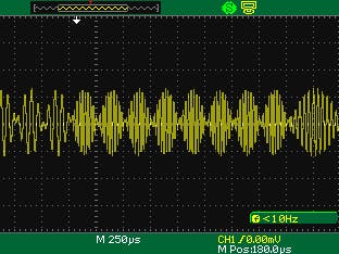
The next step is to monitor and measure the physical signals of the digital circuit that has been implemented on the FPGA board. FH signal and Spreaded signal are measured using each of Digital Storage Oscilloscope (DSO) and Spectrum Analyzer. Figure 5 and Fig. 6 show the FH signal is measured by the DSO. While in Fig. 7 and Fig. 8 the Spreaded signal is recorded.
Then, Spectrum Analyzer is used to visualize the spectral components of the Spreaded signal as shown in Fig. 9 below. The first two hops, 16 kHz and 24 kHz, are near the spectrum Analyzer starting point (9 kHz), so they have lower amplitude than the others on the Spectrum Analyzer.
- System Features
The main features of the FHSS system model that is based by FPGA are:
· Produce 500 hops/sec.
· Design flexibility, for example, it is possible to increase the hopping rate up to 16000 hops/sec in this system, just by changing only one number by HDL code.
· Has 7 different frequencies (Hops).
· The spacing between one frequency and another is 8 kHz.
· The data rate is 1 kbps.
· The system occupies a band of 48 kHz.
- References:
[1] R. C. Dixon, Spread Spectrum Systems with Commercial Applications, Third Edit. Wiley-Interscience Publications, 1994.


Comments