

Hardware components | ||||||
 |
| × | 1 | |||
| × | 1 | ||||
Let's try hacking the electric cooker with the explanation.
What is a Suvid Machine?The Suvid Machine is a recipe made a long time ago, and in 1799, the British Count Benjamin Thompson theoretically devised the first method of cooking, a recipe that warms food in a sealed plastic bag for long periods in warm water.
However, due to practicality such as cost of cooking, time, etc., it is not used positively.
Ingredients cooked with a Suvid machine preserve texture deformation, nutritional preservation, taste, form and juice, and are particularly excellent for producing soft texture in meat. It has the advantage that the loss of nutrients can be minimized because it is cooked at low temperature.
The disadvantage is: the price is very expensive. I have not been able to buy it for over 2 million won. Nowadays, for the household use, a water bead machine with a price of 200,000 won has been started to be installed in the cooking pot. There are not many kinds and there is a disadvantage that it can not heat a large amount of materials.
Ohm's law is inverse, so the heater capacity is estimated to be about 1 kilo watt.
220V / 220V / 43.5 ohms = about 5.057A
Voltage x Current = Power
220V x 5.057A = 1112W
I searched the internet and found the electricity consumption in the electric cooker specification is similar to 1100W. The heater capacity of 1100W does not seem to be sufficient for use as a bead machine. The heater may not work even if once you connect the 220V to the alligator clip to see if the heater works.
I have been touching it for a few seconds with the power supply and it turns out to be hot. Completion of testing of most parts in electric cooker.
1.77 inch TFT LCD operation successful. Standard LCD display provided by Arduino. Simple operation successful but the screen size is too small. Since Arduino is basically a TFT LCD, there is no need to add a library and it is easy to program. It is not enough to display all the desired temperature and time warning messages. I need to find a larger TFT LCD. If you want to display only the temperature information, you can use O.K.
2.4 inch TFT LCD Hacking ...
I bought a TFT LCD in China and the price is cheap, but there is no description, no test program or driver ...
I downloaded the program from the site I found by asking my brother, but it does not work ...
There's no doubt about the hardware misplacement of the Arduino shield, but ...
I suspected it was defective and changed the board and LCD module, but still do not work ...
The ones that sent text to the serial monitor are well visible ...
Compiling and uploading seems to be OK ...
Make sure that the size and shape of the product photos are the same on the downloaded site.
I do not know, I looked up Driver IC, and I can not tell because the IC is not coming out ...
I was worried for a while ...
Alas, TFT LCD was disassembled ...
To find the IC number ...
But...
I did not see the IC even though I disassembled it all ...
Fixed LCD problem that has long been deceived ...
After a few days of hardship, I found out ...
TFT LCD photo floating on the internet is same ...
There are two different types of driving ICs ...
In the manufacturer, the drive IC is called SPDF5408, but ...
In fact, the driver called ILI9341 was built ...
The driver is totally different.
The operation succeeded after replacing the library ...
Today's lesson ...
If you do not have a datasheet ... you will have to fight with lots of shits .
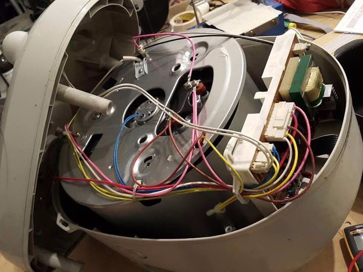
Disassembled the rice cooker sensor ...
I tried to disassemble the sensor to determine the part number of the thermistor.
It is tightly sealed, giving up the opening ...
If you have spare parts, I will open them even if i break them ...
It is not easy to obtain parts like this ...
If you fail to hack the thermistor value, consider replacing it with a known temperature sensor ...
Hacking the thermistor and temperature characteristics makes the hardware easier, while the software gets more complicated, while connecting the temperature sensors I know will make the hardware simpler but software easier ...
This problem will be determined after the temperature thermistor hack ..
The most inconvenient and unfortunate part of operating the TFT LCD is the font ...
The default fonts are based on an unsightly unsightly font in the old block breaking game, though the letters are a bit bigger ...
I was pretty good with Arduino (the Arduino instructor and long-time programmers) and I asked them how to use fonts that are nice to them ...
It's hard to get fonts, especially if you want to use Hangul ...
I asked a friend who was writing a part of the program at the Merkurton convention to look for a pretty-looking font. I spent a lot of time looking for it, but it was not so common that I finally found it.
I asked to create a font to fit the screen ...
Shaking his head ...
Nogada does not have such a nogada ...
finally...
I made it myself ...
It is convenient to use the utility as a bit image but it is too slow because the LCD is low so it is hard to display it as a bitmap ...
I draw the coordinates by using the relatively fast Line command ...
To make matters worse ...
Each segment of the 7 segments in the screen design received by the designer did not match the shape of each of the segments.
(Originally, I have to work with the designer again to get the coordinates of the segments and the coordinate values that are located in them ... I think the designer is too busy,
The code is as complex and long as a mop, thanks to ...
The time was devastated ...
depending on...
We have matched segments and numbers using arrays ...
I wrote a very simple automata ...
I feel burdened with the first project of Arduino ...
Since you have registered the test program in the attachment file, please download and run it if you need it ...
The program is long ...
The trap looks dirty and complicated ...
// Define the TFT LCD digit segments from 0 - 9
byte seven_seg_digits[10][7] = { { 1,1,1,1,1,1,0 }, // = 0
{ 0,1,1,0,0,0,0 }, // = 1
{ 1,1,0,1,1,0,1 }, // = 2
{ 1,1,1,1,0,0,1 }, // = 3
{ 0,1,1,0,0,1,1 }, // = 4
{ 1,0,1,1,0,1,1 }, // = 5
{ 1,0,1,1,1,1,1 }, // = 6
{ 1,1,1,0,0,0,0 }, // = 7
{ 1,1,1,1,1,1,1 }, // = 8
{ 1,1,1,1,0,1,1 } // = 9
};
int Diff_c_y = 30; // Difference y is 30 pixel for segment c
int Diff_d_y = 60; // Difference y is 60 pixel for segment d
int Diff_c_y_low = 10; //
int Diff_d_y_low = 20; //
int MoveX_low = 19; // Move to 18 pixel to right
int MoveX = 46; // Move to 46 pixel to right
void loop()
{
while(1)
{
seven_seg_set_temp_high_byte(8,WHITE);
seven_seg_set_temp_low_byte(8,WHITE);
seven_seg_now_temp_high_byte(8, WHITE); // present temp, upper byte LCD screen display CLEAR
seven_seg_now_temp_low_byte(8, WHITE); //
present temp, lower byte LCD screen display CLEAR
for (int i=0; i<10; i++) {
seven_seg_set_temp_high_byte(i,RED); //
present temp, upper byte LCD screen display
seven_seg_set_temp_low_byte(i,RED); //
present temp, lower byte LCD screen display
seven_seg_now_temp_high_byte(i, BLUE); //
present temp, upper byte LCD screen display
seven_seg_now_temp_low_byte(i, BLUE); //
present temp, lower byte LCD screen display
delay(1000);
seven_seg_set_temp_high_byte(i,WHITE);
seven_seg_set_temp_low_byte(i,WHITE);
seven_seg_now_temp_high_byte(i, WHITE); //
present temp, upper byte LCD screen display CLEAR
seven_seg_now_temp_low_byte(i, WHITE); //
present temp, lower byte LCD screen display CLEAR
} //for
} // while
} // end of loop
//
set temp, LCD screen display
void seven_seg_set_temp_high_byte(byte HighByte, int COLOR) {
byte segCount = 0;
// for (byte segCount = 0; segCount < 7; ++segCount) {
set_high_byte_segment_a (seven_seg_digits[HighByte][segCount], COLOR);
segCount++;
set_high_byte_segment_b (seven_seg_digits[HighByte][segCount], COLOR);
segCount++;
set_high_byte_segment_c (seven_seg_digits[HighByte][segCount], COLOR);
segCount++;
set_high_byte_segment_d (seven_seg_digits[HighByte][segCount], COLOR);
segCount++;
set_high_byte_segment_e (seven_seg_digits[HighByte][segCount], COLOR);
segCount++;
set_high_byte_segment_f (seven_seg_digits[HighByte][segCount], COLOR);
segCount++;
set_high_byte_segment_g (seven_seg_digits[HighByte][segCount], COLOR);
// } // for
} // end of function
//
set temp, lower byte LCD screen display
void seven_seg_set_temp_low_byte(byte HighByte, int COLOR) {
byte segCount = 0;
// for (byte segCount = 0; segCount < 7; ++segCount) {
set_low_byte_segment_a (seven_seg_digits[HighByte][segCount], COLOR);
segCount++;
set_low_byte_segment_b (seven_seg_digits[HighByte][segCount], COLOR);
segCount++;
set_low_byte_segment_c (seven_seg_digits[HighByte][segCount], COLOR);
segCount++;
set_low_byte_segment_d (seven_seg_digits[HighByte][segCount], COLOR);
segCount++;
set_low_byte_segment_e (seven_seg_digits[HighByte][segCount], COLOR);
segCount++;
set_low_byte_segment_f (seven_seg_digits[HighByte][segCount], COLOR);
segCount++;
set_low_byte_segment_g (seven_seg_digits[HighByte][segCount], COLOR);
// } // for
} // end of function
//
present temp, upper byte display
void seven_seg_now_temp_high_byte(byte HighByte, int COLOR) {
byte segCount = 0;
// for (byte segCount = 0; segCount < 7; ++segCount) {
time_high_byte_segment_a (seven_seg_digits[HighByte][segCount], COLOR);
segCount++;
time_high_byte_segment_b (seven_seg_digits[HighByte][segCount], COLOR);
segCount++;
time_high_byte_segment_c (seven_seg_digits[HighByte][segCount], COLOR);
segCount++;
time_high_byte_segment_d (seven_seg_digits[HighByte][segCount], COLOR);
segCount++;
time_high_byte_segment_e (seven_seg_digits[HighByte][segCount], COLOR);
segCount++;
time_high_byte_segment_f (seven_seg_digits[HighByte][segCount], COLOR);
segCount++;
time_high_byte_segment_g (seven_seg_digits[HighByte][segCount], COLOR);
// } // for
} // end of function
//////////////////////////////////////////////
//
present temp, lower byte display
/////////////////////////////////////////////
void seven_seg_now_temp_low_byte(byte HighByte, int COLOR) {
byte segCount = 0;
// for (byte segCount = 0; segCount < 7; ++segCount) {
time_low_byte_segment_a (seven_seg_digits[HighByte][segCount], COLOR);
segCount++;
time_low_byte_segment_b (seven_seg_digits[HighByte][segCount], COLOR);
segCount++;
time_low_byte_segment_c (seven_seg_digits[HighByte][segCount], COLOR);
segCount++;
time_low_byte_segment_d (seven_seg_digits[HighByte][segCount], COLOR);
segCount++;
time_low_byte_segment_e (seven_seg_digits[HighByte][segCount], COLOR);
segCount++;
time_low_byte_segment_f (seven_seg_digits[HighByte][segCount], COLOR);
segCount++;
time_low_byte_segment_g (seven_seg_digits[HighByte][segCount], COLOR);
// } // for
} // end of function
// -------------------------------------------------
// set temp. upper. 7 segment a
void set_high_byte_segment_a (boolean disp,int COLOR)
{
if (disp) {
for (int i=0;i < 8 ; i++) {
tft.drawLine(92+i,110+i,128-i,110+i,COLOR);
} // for
} // if
} // end of function
// -------------------------------------------------
// set temp upper 7 segment b
void set_high_byte_segment_b (boolean disp, int COLOR)
{
if (disp) {
for (int i=0;i < 4 ; i++) {
tft.drawLine(128-i,113+i,128-i,140-i,COLOR);
} // for
for (int i=0;i < 6 ; i++) {
tft.drawLine(126-i,115+i,126-i,141-i,COLOR);
} // for
} // if
} // end of function
// -------------------------------------------------
// set temp upper 7 segment c
void set_high_byte_segment_c (boolean disp, int COLOR)
{
if (disp) {
for (int i=0;i < 8 ; i++) {
tft.drawLine(129 -i,111+Diff_c_y + i,129-i,143+Diff_c_y - i,COLOR);
} // for
} // if
} // end of function
// -------------------------------------------------
// set temp upper 7 segment d
void set_high_byte_segment_d (boolean disp, int COLOR)
{
if (disp) {
for (int i=0;i < 8 ; i++) {
tft.drawLine(98-i,(108 + Diff_d_y + i),119+i,(108 + Diff_d_y + i),COLOR);
}
} // if
} // end of function
// -------------------------------------------------
// set temp upper 7 segment e
void set_high_byte_segment_e (boolean disp, int COLOR)
{
if (disp) {
for (int i=0;i < 8 ; i++) {
tft.drawLine(90+i,143+i,90+i,173-i,COLOR);
} // for
} // if
} // end of function
// -------------------------------------------------
// set temp upper 7 segment f
void set_high_byte_segment_f (boolean disp, int COLOR)
{
if (disp) {
for (int i=0;i < 4 ; i++) {
tft.drawLine(90 +i,111+i,90+i,140+i,COLOR);
}//for
for (int i=0;i < 4 ; i++) {
tft.drawLine(94+i,115+i,94+i,141-i,COLOR);
} // for
} // if
} // end of function
// -------------------------------------------------
// set temp upper 7 segment g
void set_high_byte_segment_g (boolean disp, int COLOR)
{
if (disp) {
for (int i=0;i < 4 ; i++) {
tft.drawLine(98-i,140+i,121+i,140+i,COLOR);
} //for
for (int i=0;i < 4 ; i++) {
tft.drawLine(94+i,144+i,124-i,144+i,COLOR);
} //for
} // if
} // end of function
// ============================================================
// set temp lower
//=============================================================
// -------------------------------------------------
// set temp lower 7 segment a
void set_low_byte_segment_a (boolean disp, int COLOR)
{
if (disp) {
for (int i=0;i < 8 ; i++) {
tft.drawLine(92+MoveX+i,110+i,128+MoveX-i,110+i,COLOR);
} // for
} // if
} // end of function
// -------------------------------------------------
// set temp lower 7 segment b
void set_low_byte_segment_b (boolean disp, int COLOR)
{
if (disp) {
for (int i=0;i < 4 ; i++) {
tft.drawLine(129+MoveX-i,111+i,129+MoveX-i,139+i,COLOR);
} //for
for (int i=0;i < 6 ; i++) {
tft.drawLine(126+MoveX-i,115+i,126+MoveX-i,141-i,COLOR);
} //for
} // if
} // end of function
// -------------------------------------------------
// set temp lower 7 segment c
void set_low_byte_segment_c (boolean disp, int COLOR)
{
if (disp) {
for (int i=0;i < 8 ; i++) {
tft.drawLine(129+MoveX-i,111+Diff_c_y + i,129+MoveX-i,145+Diff_c_y - i,COLOR);
} // for
} // if
} // end of function
// -------------------------------------------------
//
set temp lower
7 segment d
void set_low_byte_segment_d (boolean disp, int COLOR)
{
if (disp) {
for (int i=0;i < 8 ; i++) {
tft.drawLine(98+MoveX-i,(108 + Diff_d_y + i),119+MoveX+i,(108 + Diff_d_y + i),COLOR);
} // for
} // if
} // end of function
// -------------------------------------------------
//
set temp lower
7 segment e
void set_low_byte_segment_e (boolean disp, int COLOR)
{
if (disp) {
for (int i=0;i < 8 ; i++) {
tft.drawLine(90+MoveX+i,143+i,90+MoveX+i,173-i,COLOR);
} // for
} // if
} // end of function
// -------------------------------------------------
//
set temp lower
7 segment f
void set_low_byte_segment_f (boolean disp, int COLOR)
{
if (disp) {
for (int i=0;i < 4 ; i++) {
tft.drawLine(90+MoveX+i,111+i,90+MoveX+i,140+i,COLOR);
} // for
for (int i=0;i < 4 ; i++) {
tft.drawLine(94+MoveX+i,115+i,94+MoveX+i,141-i,COLOR);
} // for
} // if
} // end of function
// -------------------------------------------------
//
set temp lower
7 segment g
void set_low_byte_segment_g (boolean disp, int COLOR)
{
if (disp) {
for (int i=0;i < 4 ; i++) {
tft.drawLine(98+MoveX-i,140+i,121+MoveX+i,140+i,COLOR);
} // for
for (int i=0;i < 4 ; i++) {
tft.drawLine(94+MoveX+i,144+i,124+MoveX-i,144+i,COLOR);
} // for
} // if
} // end of function
// ============================================================
// present temp upper byte
//=============================================================
// -------------------------------------------------
//
present temp upper byte
7 segment a
void time_high_byte_segment_a (boolean disp, int COLOR)
{
if (disp) {
for (int i=0;i < 3 ; i++) {
tft.drawLine(210+i,149+i,224-i,149+i,COLOR);
} // for
} // if
} // end of function
// -------------------------------------------------
//
present temp upper byte
7 segment b
void time_high_byte_segment_b (boolean disp, int COLOR)
{
if (disp) {
for (int i=0;i < 2 ; i++) {
tft.drawLine(225 -i,150+i,225-i,160+i,COLOR);
} // for
for (int i=0;i < 2 ; i++) {
tft.drawLine(223-i,152+i,223-i,161-i,COLOR);
} // for
} // if
} // end of function
// -------------------------------------------------
//
present temp upper byte
7 segment c
void time_high_byte_segment_c (boolean disp, int COLOR)
{
if (disp) {
for (int i=0;i < 4 ; i++) {
tft.drawLine(225 -i,151+Diff_c_y_low+i,225-i,164+Diff_c_y_low - i,COLOR);
} // for
} // if
} // end of function
// -------------------------------------------------
//
present temp upper byte
7 segment d
void time_high_byte_segment_d (boolean disp, int COLOR)
{
if (disp) {
for (int i=0;i < 3 ; i++) {
tft.drawLine(212-i,(153 + Diff_d_y_low + i),222+i,(153 + Diff_d_y_low + i),COLOR);
} // for
} // if
} // end of function
// -------------------------------------------------
//
present temp upper byte
7 segment e
void time_high_byte_segment_e (boolean disp, int COLOR)
{
if (disp) {
for (int i=0;i < 4 ; i++) {
tft.drawLine(209+i,162+i,209+i,174-i,COLOR);
} // for
} // if
} // end of function
// -------------------------------------------------
//
present temp upper byte
7 segment f
void time_high_byte_segment_f (boolean disp, int COLOR)
{
if (disp) {
for (int i=0;i < 2 ; i++) {
tft.drawLine(211+i,152+i,211+i,162-i,COLOR);
} // for
for (int i=0;i < 2 ; i++) {
tft.drawLine(209 +i,150+i,209+i,160+i,COLOR);
} // for
} // if
} // end of function
// -------------------------------------------------
//
present temp upper byte
7 segment g
void time_high_byte_segment_g (boolean disp, int COLOR)
{
if (disp) {
for (int i=0;i < 2 ; i++) {
tft.drawLine(214-i,160+i,220+i,160+i,COLOR);
}
for (int i=0;i < 2 ; i++) {
tft.drawLine(212+i,162+i,222-i,162+i,COLOR);
} // for
} // if
} // end of function
// ============================================================
//
present temp upper byte
//=============================================================
// -------------------------------------------------
//
present temp upper byte
7 segment a
void time_low_byte_segment_a (boolean disp, int COLOR)
{
if (disp) {
for (int i=0;i < 3 ; i++) {
tft.drawLine(210+MoveX_low+i,149+i,224+MoveX_low-i,149+i,COLOR);
} // for
} // if
} // end of function
// -------------------------------------------------
//
present temp upper byte
7 segment b
void time_low_byte_segment_b (boolean disp, int COLOR)
{
if (disp) {
for (int i=0;i < 2 ; i++) {
tft.drawLine(225+MoveX_low-i,150+i,225+MoveX_low-i,160+i,COLOR);
} // for
for (int i=0;i < 2 ; i++) {
tft.drawLine(223+MoveX_low-i,152+i,223+MoveX_low-i,161-i,COLOR);
} // for
} // if
} // end of function
// -------------------------------------------------
//
present temp upper byte
7 segment c
void time_low_byte_segment_c (boolean disp, int COLOR)
{
if (disp) {
for (int i=0;i < 4 ; i++) {
tft.drawLine(225+MoveX_low-i,151+Diff_c_y_low+i,225+MoveX_low-i,164+Diff_c_y_low - i,COLOR);
} // for
} // if
} // end of function
// -------------------------------------------------
//
present temp upper byte
7 segment d
void time_low_byte_segment_d (boolean disp, int COLOR)
{
if (disp) {
for (int i=0;i < 3 ; i++) {
tft.drawLine(212+MoveX_low-i,(153 + Diff_d_y_low + i),222+MoveX_low+i,(153 + Diff_d_y_low + i),COLOR);
} // for
} // if
} // end of function
// -------------------------------------------------
//
present temp lower
7 segment e
void time_low_byte_segment_e (boolean disp, int COLOR)
{
if (disp) {
for (int i=0;i < 4 ; i++) {
tft.drawLine(209+MoveX_low+i,162+i,209+MoveX_low+i,174-i,COLOR);
} // for
} // if
} // end of function
// -------------------------------------------------
//
present temp lower
7 segment f
void time_low_byte_segment_f (boolean disp, int COLOR)
{
if (disp) {
for (int i=0;i < 2 ; i++) {
tft.drawLine(209+MoveX_low+i,150+i,209+MoveX_low+i,160+i,COLOR);
} // for
for (int i=0;i < 2 ; i++) {
tft.drawLine(211+MoveX_low+i,152+i,211+MoveX_low+i,162-i,COLOR);
} // for
} // if
} // end of function
// -------------------------------------------------
//
present temp lower
7 segment g
void time_low_byte_segment_g (boolean disp, int COLOR)
{
if (disp) {
for (int i=0;i < 2 ; i++) {
tft.drawLine(214+MoveX_low-i,160+i,220+MoveX_low+i,160+i,COLOR);
} // for
for (int i=0;i < 2 ; i++) {
tft.drawLine(212+MoveX_low+i,162+i,222+MoveX_low-i,162+i,COLOR);
} // for
} // if
} // end of function
<Temperature timer setting bar Heater reservation button operation test>
The set temperature was programmed to display the current time with the temperature setting and temperature graph ...
In order to be intuitive to understand at a glance, the screen design has graphically displayed the temperature and the remaining time. When heating, when the heater is reserved, the reservation LED is lit as an LED, which is also relatively faster than the bitmap (Square, circle) using ...
The source code is attached to the ...
Yesterday I had an all day trouble adding an all day library ...
There are a few things I found out ...
first,
Arduino does not need to add a library and then re-run it after finishing the sketch.
second,
I put a compressed file or folder in the Program Files (x86) \ arduino \ libraris directory ...
This folder is the directory used by the Aduno system ...
Library \ Documents \ Arduino \ libraries directory and add it to sketch -> Include Library -> Add zip library ...
I just downloaded the library from gitHUB without thinking ...
I noticed that the contents of the files may be different for each library. (Very important)
I have to do a lot of unnecessary tasks that can not be done because of this thing .. (ㅠ. ㅠ)
Once I solved the library problem ...
Another problem ...
I was writing a program and suddenly a strange message appeared ...
You can zoom in on the message screen ...
Message that the sketch (source file) is too big to compile ...
There are a lot of programs to be used in the future. I have already used all the memory, so I need to reduce the program size.
dump....
I sat down ...
Looking at the sky ...
I lost my say ...
Now how do you ...
I'm going back to my hardware troubles when I selected LCD again ...
You can use the Aduno Mega ...
If you attach it to the front of the rice cooker as originally planned, the size is too big and the TFT LCD is biased to one side.
The head gets complicated ...
< A Fundamental Reconsideration on Arduino Board ... >
Can Bead sous vide Can Bead Machine
After compilation error due to over capacity on the Aduno Uno board ...
We are rethinking the use of the Arduino Mega Board after a hard time ...
At first, the Arduino Mega Boards were bigger than Uno, and since they were sticking out laterally after mounting the TFT LCD, I did not use them in terms of mechanism.
As the program capacity became a problem, we began reviewing again ...
Once I plugged the pin array into the mega board ...
It did not work ...
For sure...
Friends who have a lot of experience on the Internet or Arduino told me that Shield is compatible without any action ...
In addition, looking at the circuit diagram, three D ports (PD4, PD5, PD6) were not connected to the circuit at all and were open. (I could not understand ... If you do not connect these three pins, Maybe it does not seem to be compatible.)
One site on the Internet says that Uno and Mega are fully compatible (http://kevinrye.net/index_files/arduino_mega_2560.php) ...
It seems that they didn't test all the compatibility tests, that only the LED flashes or the program is uploaded ...
ArduinoMEGA_0146-6
In the uno board, as shown in the above pin layout diagram, are PD0 ~ PD7 connected to pins 0 ~ 7?
PD0 ~ PD7 are not used as simple I / O inside the CPU, but they seem to be used as a data bus, so that they feel more inevitable ...
There are two ways to try
First, how to redefine the pin by considering the pin layout in the program and ...
Secondly, it is a way to physically disconnect the hardware by reconnecting the hardware and disconnecting the shield.
But the first way is to redefine the pin layout without touching the hardware, but it seems like PB0 ~ PB7 are used as data bus ...
I thought I might have a subtle impact on timing ...
The second method is that the PD4 ~ PD6 3 pins can not be connected to the pin connector on the CPU.
I also search for articles related to mega ...
I have also found a post that Mega Shield will not be compatible with Uno because it runs at 3.3V ...
I thought that it would be better to change the Uno to Mega even if I fix the whole device once ...
If you have experience with this, please advice ... Black ... Black ... ㅠ. ㅠ.
Various components of electric rice cooker (heater, switch, sensor, etc.) are used as they are but ...
The control circuit, including the CPU, is supposed to be programmed with the Arduino ...
In the rice cooker, pull out the module with the motherboard fixed and ...
Unscrew the fixing screw and ...
Cut all connected wires, including connectors ...
Remove the motherboard ...
The front panel requires the switch to be used as is, so without removing the PCB ...
The TFT LCD will be fixed in padded format ...
Arduino mega board and power unit (5V switching power, 12V switching power) and SSR for controlling the heater are directly measured and arranged, and the device is designed ...
Red is going to cut with laser cutting machine ...
I plan to mark only green without cutting ...
Since the size of the main board is the same as that of the main board, it is possible to match the sizes exactly by screwing the components together and then joining them again.
The tool design is written in Rhino, a 3D modeling tool, and is attached to the file in Rhino format.
When the key input is received from all microcontrollers, chattering (vibration caused by the machine when the contact of the switch is opened or closed.) When the switch is turned on or off, the intermittent state is repeated due to the vibration of the contact point. If this happens, the same character will be shot multiple times.)
There are two ways to do this ...
The first is the combination of the capacitor and the resistor by the hardware method, and the method of absorbing the appearance of the voltage when the chattering occurs in the capacitor and ...
Secondly, it detects the change of the input value by the method of software, measures the time at that point, compares it with a predetermined time (Debounced delay), and distinguishes whether chattering or normal key input is performed. It has the disadvantage of having to write it, but it does not have to use parts, so it has the advantage of simpler hardware and less material cost ...
This project also needs to take measures against Debounce because it gets taller.
I experimented with simple circuits as shown in the picture above ...
Press the key once to turn on the LED ...
Press again to turn off ...
Well, it worked fine ...
Please refer to the attached file for the program source ... debounce.test
Arduino and TFT LCD Shield Fixture to be attached to the front of the rice cooker ...
Combined with Arduino and Shield, it was designed and printed as a 3D printer for fixing to the front of the electric cooker ...
Hye Hye helped the maker ...
The first output will reflect the revision of some of the fixtures and output one more time ...
Because the front part of the rice cooker is rounded, the inside of the equipment is designed so that it gets a little bit ... (It was supposed to output the supporter so that the equipment could be rounded.
After attaching Arduino and TFT LCD shield to the instrument and fixing it ...
The front side of the TFT LCD is laser-cut and fixed to the front to hide the dirty content ...
I put it on the front of the rice cooker ...
It fits exactly to the curve ...
At last, we operate TFT LCD on Arduino Mega Board ...
Meantime...
We have the wrong information that Aduino Megaboda is fully compatible (Pin to Pin) with Aduino Uno board.
After a lot of hard work ...
The connection to the mega board was successful ...
But rather than the joy of setting ...
I spent a lot of time trying to find cause ...
Like...
If you do an investigation with the real criminal ...
Like I can not catch the killer after all ...
It is a lethal mistake that the Uno and Mega Boards are fully compatible ...
The detailed analysis of the circuit diagram of Aduno Uno and Megaboard ...
The definition and arrangement of the pins as well as the number of pins were also very different ...
So ...
Give up the shield ...
I was able to find the pins and connect them ...
In the program, I have found all pin definitions and matched them ...
The most worried data bus in the process is the 8-bit data ...
Fortunately, I was able to connect using Port A ...
When I traveled to Jeju Island ...
I was thinking all over the TFT LCD ...
I did not have any sightseeing .... ㅠ. ㅠ.
My good time ...
Modify the SD interface settings on the Arduino Mega Board ... ...
As I explained in my previous story ...
The TFT LCD Shield for Arduino Uno has been operated by setting and changing the hardware pin connection ...
The image on the SD card does not come up on the TFT LCD ...
Uno and hardware pins were matched 1: 1 with pin numbers (10, 11, 12, 13) ...
Does not work ...
again...
Looking at the schematics of Uno and Mega ...
Apart from the pin number, the function for communicating with the SD card was differently mapped to the pin number ...
After moving the pins, normal operation ...
Unomega
10 -> 10 times
11 -> 51
12 -> 50 times
13 -> 52
conclusion
Arduino mega differs from Uno in circuit and pin arrangement is completely different ...
However, I have installed a port to absorb the functions of Uno, but it is not pin to pin compatible ...
After all, it's a natural story ...
Shield for Uno does not work even if it is attached to mega board ...
Software Timer Interrupt Coding......
Whether LED blinks on a bead machine or makes repetitive movements at a fixed time ...
There are two ways of causing a hardware interrupt to be executed every predetermined cycle by a hardware interrupt so that a specific routine is executed and a method by software interruption.
The hardware-based method can be advantageous when the interrupt situation or condition is complicated, but ...
In this case, I have created an interrupt service routine that is called once per second, because it only requires a simple timer interrupt such as time setting, LED blinking, and setting value blinking in the TFT LCD setting.
What should be noted here is ...
MsTimer2.h, a timer library that worked normally in Arduino Uno, did not work on mega and it took a lot of time ...
I found that the Mega and the Uno are very different from each other in hardware such as the pin assignment, but I have learned from previous experiments.
In this test program, I noticed that the library is also not compatible with the board ...
So if you are using a megaboard, you should use a header file that works on the megaboard that you uploaded as an attachment file ...
The test program is ...
Flashing the LED every 1 second ...
Serial port to current seconds ...
Output every minute and minutes ...
A test program that displays the hour when time passes ...
If you use it as a timer, you will have to input the setting value and count down.
Present temperature display with RGB LED ...
If the bead lid cuts acryl and engraves letters and changes the color of the lid according to the current temperature ...
Even at a distance, I was able to carry a certain temperature even if I looked at the color of the lid.
I have enjoyed two kinds of effects: interior fun and practicality ...
First, the RGB LED operates at 12V, and the GPIO of the Arduino is about 5V, so there is not enough voltage or current to drive it directly.
So I connected the FET to drive the RGB LED ...
Theoretically, you have to operate with the above circuit only ...
It does not work because it actually connects ...
As shown in the above data sheet, it is said that about 4.5A of current can flow about 10A.
The solution is to use one more FET ...
But...
In order to drive the RGB LEDs, the circuit must be more complicated because there are three more circuits ...
Plan to run with ULN2003 changed ...
I did not change the brightness of the LED, and after a long time ...
All digital I / O pins were not PWM capable and I / O ports were moved and working normally ...
Now we are slowly seeing the end of this project ...
Just a little more ...
The hardware is more than 90% complete ...
Please note that the test program is uploaded as an attachment file ...
Most mobile phone charging adapters available today do not have a coupling screw ...
Cutting forcing by attaching cutting tool to Dremel ...
After forcibly removing the lid ...
The board was removed ...
The AD-DC converter with a capacity of 0.42A is selected as the 12V power supply.
I chose the small size ...
You can measure the size of the motherboard by ...
I designed the machine so that I can cut the laser in the same size as the main board ...
.
I printed out the actual size of the printer and put each part on it.
The hole positions for fixation were precisely matched ..
Present temperature display with RGB LED ...If the bead lid cuts acryl and engraves letters and changes the color of the lid according to the current temperature ...
Even at a distance, I was able to carry a certain temperature even if I looked at the color of the lid.
I have enjoyed two kinds of effects: interior fun and practicality ...
First, the RGB LED operates at 12V, and the GPIO of the Arduino is about 5V, so there is not enough voltage or current to drive it directly.
So I connected the FET to drive the RGB LED ...
Theoretically, you have to operate with the above circuit only ...
It does not work because it actually connects ...
As shown in the above data sheet, it is said that about 4.5A of current can flow about 10A.
The solution is to use one more FET ...
But...
In order to drive the RGB LEDs, the circuit must be more complicated because there are three more circuits ...
Plan to run with ULN2003 changed ...
I did not change the brightness of the LED, and after a long time ...
All digital I / O pins were not PWM capable and I / O ports were moved and working normally ...
Now we are slowly seeing the end of this project ...
Just a little more ...
The hardware is more than 90% complete ...
Please note that the test program is uploaded as an attachment file ...
Create AIDINO Mega Bead Shield # 1I made a shield board for Arduino Mega ...
Soldering is done by aligning the connectors that can be connected to the Arduino Mega Board.
Cutting with angle saw ...
Solder all the way to Teflon wire ...
Try running the test program ...
Action successful ...
Key setting and status transition diagram for numerical bead machine operationThe button key attached to the rice cooker differs from the use of a bead machine ...
So ...
Some buttons (start button) are made of thin metal and added ...
The rest is to use the same key as it is ...
The state transition diagram below is ...
It tells you the status change of which button to press when from standby to do the next action ...
I can not think of it as final because I just saw it as I thought.
It may change according to future situation ...
I need a switch to run a bead machine ...
In this project ...
Hack the switch on the front of the rice cooker and use it ...
Hacking and tracing PCB board pattern and connecting to each connector by detecting position and connection point of each switch ...
Solder the points of each connector and use the shrink tubing to clean the wires ...
see...
Now you can use the front switch of the rice cooker as it is ...
The pin number of the Arduino Mega is
Connect 7 pins by setting input pins to 30, 31, 32, 33, 34, 35, 36 ...
About temperature sensing ...The electric rice cooker (naturally) also has a temperature sensor ...
If you can use this temperature sensor ...
In fact, the ...
because...
It is the most advantageous that there is a sensor at the position where the temperature sensing is the best in terms of mechanism,
However, if you want to use a temperature sensor that is mounted on an electric cooker ...
Hacking the temperature characteristics of a temperature sensor that is not open at all and reverse it ...
It is necessary to find out the change of the resistance value of the sensor and the temperature of the rice cooker while giving the temperature change.
So ...
Using the LM35 temperature sensor, which includes temperature characteristics and data sheets as well as source code, the coding is very simple and ...
There is no need to calibrate the temperature and the values received on the analog input ... (there is a calculation formula for reading the temperature).
And if you use three temperature sensors ...
Because the number of sensors is large, we can find more accurate temperature values ...
If one or more temperature sensors fail during operation, a warning message may be issued ...
In fact, when I connected the sensor, one of the three temperature sensing values is read differently from the two,
I tried to melt the silicon with the silicone gun after attaching the bond.
Three problems ...
first...
The switch that recognizes that the rice cooker is put on because of applying the bond did not work well ...
second...
I searched the internet and it was hard to use due to the possibility of melting due to the heat generated when the silicon melts at low temperatures.
Finally, the third ...
I actually connected to Arduino and measured the temperature and output it with Serial.print function ...
The three sensors (T1, T2, T3) have similar measured values ...
The temperature on the front of the rice cooker and the temperature of the back of the rice cooker with three sensors were very large. I could not read the correct temperature as shown in the picture above.
The situation is like this ...
I can not help it now ...
The previous temperature sensor was needed again ...
I contacted the electric cooker manufacturer in a hurry and asked if I could buy only the temperature sensor.
I'm not ...
If you sell parts to a consumer, you may have a material or an accident, so we do not sell it at our headquarters ...
I went to the center and assessed it. (I had experience working at a large research institute, so I could design an electronic circuit and write a note if necessary.
Removing existing sensors and ...
Replace the newly purchased temperature sensor ...
I connected the removed sensor to Arduino and wrote the program and checked the temperature value.
Temperature drifts up to 2 degrees ...
It may be because of the noise on the analog input ...
How to reduce the noise by delaying or taking an average value when reading the temperature in the program ...
How to use IR filter ...
You can implement a method of reducing noise by connecting a capacitor to an analog reference voltage.
In conclusion...
I decided to use the temperature sensor in the existing rice cooker and ...
It seems that there is a need to reduce the deviation of the temperature values measured by the hardware and software methods and increase the accuracy.
Complete mainboard ...The main board is finished ...
First, I used the laser cutter to mark the outline and fix the name of each part to fix the SSR which controls the heater of 5V, 12V and the rice cooker of Arduino Mega ...
Place each part in the outlined position so that the position of the fixing hole matches the part placement and wiring.
Think of the wiring path so that wiring is as short as possible and the associated parts are the shortest distance ...
By securing a hexagonal column nut on an acrylic plate, space is secured in the hole (middle portion) where the entire board is fixed by keeping the Arduino Mega Board in close contact with the acrylic.
Even if there is a fever in Adu-no-Mega, it gives a space to allow air to flow in, giving room for heat to escape ...
In each hole, make a screw groove with a tapping drill blade so that the bolt can be fixed even if there is no other nut.
Tapping all the holes and ...
Fix parts on board ...
Wires that are likely to be shorted are put in a shrink tube to heat them all to a safe state.
Tie the wires to the rack ...
Mainboard Board Completion ...
Using SSR for heater on off ...In order to turn off the heater of the rice cooker, we have to use relay or SSR (Solid State Relay) ...
Rather than using relatively inexpensive relays, we will use SSR ...
I chose SSR because ...
First, it does not sound when it is turned on ...
Second, the switching noise is very small compared to the relay when it is turned on.
Third, Debouncing Noise noise is very low on On Off ...
Fourth, the output from the Arduino digital pin can be driven without a separate component or circuit ...
Test on On Off by connecting 220V incandescent lamp instead of heater ...
Hack the temperature sensor in the rice cooker ...
The temperature sensor in the rice cooker has no information ...
This is because data sheets can not be found because part model numbers are not known either ...
Therefore, if you want to use unknown parts, you have to hack ...
To measure the temperature, we connected a precision thermometer and a voltmeter to measure ...
The temperature is continuously raised, and the measured value is output to the serial monitor for each temperature, and each value is recorded.
By turning on the heater and continuously raising the temperature, the temperature and the voltage across the analog input pin (A / D converter) are measured and plotted and analyzed ...
The circuit is ...
Connect a 15K ohm resistor in series to the temperature sensor of the rice cooker to obtain the output voltage at the intermediate connection point ...
Connect parts to a small breadboard and measure the relationship between temperature and voltage ...
The data values in the graph above are manually entered by hand.
I would like to use a program to automatically import the measured data into Excel, but ...
There is an error because there is not enough time ...
Calculate the temperature value in the Arduino based on the measured value of the graph ...
Arduino Mega Shield Making # 2
Making the last bead shield # 1 was the wiring to connect the TFT LCD ...
Temperature sensor, heater control, RGB LED connection, 12V power supply, 5V power supply, connector wiring for switch input of front panel of rice cooker was added ...
Electric rice cooker on analog pin Connector for connecting 1 temperature sensor and 3 separate temperature sensors Electromagnetic rice cooker Temperature sensor 2 pin, Temperature sensor 5V Power 1 pin, Each sensor output 3 pin, GND 1 pin Total 7 pin connector required .
Electromagnetic cooker switch input connects to digital pin 30 ~ 37 ...
The 12V power supply supplies the output of the AD-DC converter to the shield board through a 2-pin connector. The SSR control is controlled via pin 11 of the digital pin and the RGB LED is controlled by 12V with ULN2003.
Since the FET that I connected last time had to write another FET one more because of the driving voltage, I plan to use relatively cheap and simple UNL2003 ...
It supplies 12V to the pin 8 and pin 9 of the above semiconductor chip and connects the three outputs connected to the three inputs to the RGB LED ...
Finally...
On the TFT LCD side, use a universal board to solder the connector wires and connect them to the bead shield ...
Answers to questions about the Suvid Machine ...I met a reader who accidentally saw all my bead machine making machines ...
The reader asked two questions ...
The first is whether the sensed temperature is changing and how to cope ...
The second question was, like other machines, why not circulate water ...
The answer to the first question is ...
As I mentioned in the previous story, there was a temperature error ...
In the Arduino circuit, there was no noise reduction or compensation circuit for this noise ...
If you need to do this, you have to make it in the shield ...
I can solve some of the hardware ...
Software can also calibrate and reduce noise ...
Use the IR filter algorithm we talked about in the previous story ...
By reading a number of temperature values and then averaging them, it will be possible to use a low pass filter consisting of a capacitor and a resistor in the hardware ...
Answer the second question ...
Since we are planning to cover the lid in the process of remodeling the electromagnetic rice cooker that is currently being manufactured, it is difficult to arrange the components and components that can circulate the water with the pump etc. ...
The pressure cooker's pot is much thicker than the water tank thickness of a general water bead machine, so heat transfer and blocking are relatively good.
Actually, even if you measure the four corners and the center with a precision thermometer (see the figure below), there is no need to make the flow of water because there is not much temperature difference.
If the temperature difference inside the pressure cooker is large, is not the temperature difference enough to make rice delicious?
but...
If you make a large number of bead machines with a large tank size, you may need to consider this because the temperature difference can be severe.
Arduino Mega Shield Board, who was doing his own work well, did not suddenly start to work after his friends came and visited him.
It is not easy to debug while tracing the wiring, since there is a lot of wiring and bad eyes ...
If you make the PCB and upload the file at this opportunity ...
If there are those who would like to follow up later, I think I can easily follow it without wires.
(Of course I have never seen PCBs before ... I mean, it takes a lot of time to make it because I have to make it while studying from the beginning ...)
Circuit design tools are very expensive to purchase formally ...
Of course you can use it in the dark path, but ...
I am studying Ki-CAD because I think it will be possible to do a lot of work using Ki-CAD, which is an open project base.
I first drew the circuit as shown below ...
It's a circuit. There's nothing particularly difficult ...
just...
Work done by soldering all day ...
Printed on the board, I get a little hands on the work ...
Once you have made it, you can use it without hesitation.
ULN2003 does not have a library in Ki-CAD.
The measurement temperature is slightly unstable when I measure the temperature through the Adouino shield ...
I have measured the analog reference voltage with the oscilloscope I have ...
The reference voltage is shaken ...
We have added a circuit to reduce the noise by attaching a low pass filter to the capacitor on the Aduinomega shield board ...
I plan to experiment later on how useful this project is.
Please note that the circuit and ULN2003 library are attached files.
Arduino Mega Shield PCB Production # 2In the completed schematic, each device is numbered with annotate schematic components ...
Electrical Rule Check finds errors in circuit connection and completes the preparation of PCB by creating NET list ...
After drawing PCB outline (PCB cutting line) ...
I am ready to move the parts within it and prepare to play ...
Now you just need to wire ...
Arduino Shield I did not have a connector that fit exactly, so I used it to replace the hole size and spacing ...
I have heard that there is a library of Arduino Shields for Son Hojo ...
When I asked where I was, I did not know exactly where I was and I have seen it once ...
So ...
Stop working front ...
I will find the Arduino Shield Library and Foot Print and work again ...
The work files are kept in the attached file, so if you need ...
Water Bead Shield Rework # 1After a long time asking Google ...
I found the Arduino Mega Shield library ...
I used the Arduino Mega shield library to redraw the circuit from the beginning ...
In this case, to reduce the noise, we place two capacitors, 0.1uF and 100uF, respectively, in the power supply.
And I removed the pins that are compatible with the Aduino Uno ...
In the future I've considered connections that might possibly lead to additional ...
Completing the circuit and turning the Electronic Rule Check ...
I have an error like the above ...
Even if an error occurs, the NetList is generated, but ...
If you proceed without catching the error, it may cause problems such as not wiring on PCB later, so it is better to catch all errors.
As you can see above, the red circle is ...
It means that the power line shows an error ...
The meaning of the error means that there is no part connected to the power supply, and if the Power Flag is added, the error disappears ...
I fixed the error by putting the Power Flag in the place ...
I got all the errors ...
Completion of circuit diagram ...
Schematics and UNL2003 and Arduino Mega Shield library are attached files ...
Water Bead Shield Rework # 2I found the Arduino Mega shield library through the internet ...
There are a lot of Eagle libraries, but KiCAD is not much more than I thought ...
The search for the Arduino Mega Shield Library and FootPrint did not work together, so I had to work with the pin array and label to match each other ...
Once you have loaded the NetList, arrange the parts appropriately and ...
Looking at the circuit diagram, find the best place to wire the parts and replace them ...
Completed wiring ...
There are many Dip type parts and the wiring is not open ...
Considering future extensibility, we put the connector as far as possible ...
If you do not need it, you can not use it.
After finishing wiring ...
Add Filled Zone function puts copper plate on GND ...
Plate the front plate, the back plate, and finish the plate ...
It is the first production of PCB and I have finished it ...
I think I can do better if I try again next time ...
I have a few tips ...
The via hole used 38 pieces ...
I heard that there are a lot of via holes in the PCB manufacturing cost.
I found out that there was a long time ago when the size of the idle hole was very small (0.3mm or less).
In the case of PCBs like the ones we made today (0.6mm), we do not affect the unit price.
After making the production ...
Search the Internet to see if the pattern track is too thin ...
The wiring used was class 2 (0.25mm) ...
If you calculate the pattern width 0.25mm with PCB track thickness calculation program ...
I can run the current of about 535mA ...
Water Bead Shield Rework # 3Now the Suvid Shield is complete ...
We have manufactured the side board to connect the TFT-LCD with Suvid Shield ...
Actually...
I did not think I would make a side board, but after I finished the Suvid shield board, I added a circuit to the circuit diagram suddenly because I thought about the board side. I made a PCB and put it beside the bead shield PCB, Cut lines were made to order two PCBs in one.
PCB is made by placing it beside the bead shield PCB and making V-cut line for V-cut so that two PCBs can be ordered in one.
Now the bead shield related PCB is finished ...
We will make the first production, test it and fix it ...
Each gerber file is uploaded with an attachment ...
Suvid shield production # 3 (PCB order)After checking the size and component placement of the bead shield PCB ...
Now the final PCB order ...
Because the budget of the project has already been exhausted a long time and we have to save a lot of money ...
I searched for cheap places in China and got a quote ...
The quantity needed is 5 bead shields and 5 board ...
To save money, I sent an e-mail asking me to attach two PCBs and to insert a V-cut (dashed line cut by hand).
If you put a V-cut, it would be better to send two pieces separately ...
Uh ...
I have to tell you how much the price goes up ...
Decide whether or not to ...
Quote from another place ...
It seems to be manufactured in Hong Kong ...
I've been using the same PCB Gerber file in two ...
The price is almost double the difference ...
The mail came from the mail that the solder mask Gerber file was missing and I sent it again ...
I tried to attach a file to this entire story and I can not attach more than 5 files ...
So I attached a solder mask file to this story ...


Comments