

Hardware components | ||||||
 |
| × | 1 | |||
High Speed PWM Using TCC Timer/Counters
Read moreOn the Arduino with Cortex-M0 (ATSAMD21) there is more choice in frequency and speed for your PWM control than just the AnalogWrite() functions.
- Why not using Tone() function? : this function does not support you to change the PWM duty cycle.
- Why not using the AnalogWrite() function? : this function only supports one frequency ~ 490Hz
- Why not use the setPwmFrequency() function : this changes the Clock pre-scaler, possibly influencing timing of other Arduino functions for time.
It took me some efforts scrolling through fora and demo's to figure it out, so I like to share.
The difficulty is to figure out the right register settings, using the datasheet, Chapter 31 - TCC timers/counters, specific 31.6.2 for setting up the PWM counters - using GCLKC4 (not used by arduino) and connecting them to the right TCCs, and to the right IO pin.
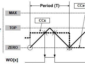
Code is self explaining, and using the dual-slope PWM mode to create glitch-free PWM signals for low (several Hz) and high speed (>>500Khz).
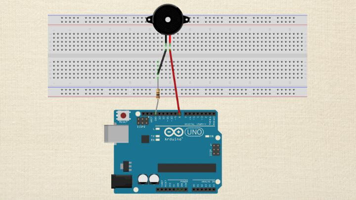
You can do a simple test by connecting a piezzo speaker to the IOs (for the audible frequencies).


Comments