

During the product development process, simulation is a key tool for analyzing the behavior and performance of complex circuits. Simulation can be used to proof basic designs, evaluate the effects of both nominal component values and variations due to parasitics, saturation and other real effects, and predict the design’s response to noise and other non-ideal inputs.
Many current industry tools for simulation are based around the SPICE (Simulation Program with Integrated Circuit Emphasis) environment. A SPICE interpreter takes text-based ‘netlists’ that include the parameters of each circuit components as well as their nodes, then translates them into matrices, differential equations, and other mathematical relations based on Kirchoff’s Laws and other physical constraints. Modern simulators generally incorporate a schematic creation tool in which the user can construct circuits using symbols with associated netlist models, and the simulator will generate a netlist based on the schematic. They also integrate a range of possible measurements and post-simulation processing tools. Both PSpice and LTSpice are such environments, owned by Cadence Design Systems and Analog Devices respectively. Each includes a native library of component models as well as the ability to import third-party component models.
In September of 2020, Texas Instruments launched a new variation of the PSpice simulator in partnership with Cadence Design Systems. It was intended to streamline the process of designing circuits with components from TI, allowing engineers to evaluate, verify, and debug circuit designs while minimizing iterations of physical prototyping. The simulator integrates a substantial native library of models of TI components. It includes automatic measurements and a number of post-processing tools including Monte Carlo and worst-case analysis. As with previous PSpice iterations, the circuit as designed in PSpice for TI can be imported directly into Cadence’s PCB design tools in order to continue the design process without needing to recreate the circuit.
This project uses TI’s PMLK Buck Evaluation Module (EVM) to demonstrate the tool capabilities. After reviewing existing references, I provide an overview of the theory involved in a buck converter. Next, I review construction of schematics of the EVM circuit in both PSpice and LTSpice, a major competing simulation tool. The next step is to demonstrate how to run various simulations on the modeled circuits: basic DC bias point checks for the various module configurations, inputs, and loads; AC frequency responses for various passive element selections; and transient output quality characterizations such as ripple characterization. Finally, I compared the simulation results with experimental data collected from the actual EVM and discuss the comparative advantages and areas of improvement for the tool.
PSpice for TI ReferencesA free download of PSpice for TI can be requested here:
https://www.ti.com/tool/PSPICE-FOR-TI
After the request is approved (likely within one day) you will receive a confirmation email with an access key. Follow the link to download the software, then run the.exe installer. In the popup, enter your TI user credentials (created during the request process) and the access key from the confirmation email, then choose a directory and wait for installation. The installation process takes less than 20 minutes.
Basic video tutorials are available on the TI website, detailing the basic workspace for schematics, simulation, and analysis.
https://training.ti.com/pspice-ti-introduction
A more detailed training course is also available through Cadence. This course includes a written guide to a number of PSpice for TI functions, beginning with basic schematic capture, then outlining the procedure for six prominent simulation types. It further discusses more complex functions such as adding parasitics and third-party models, conducting noise analysis, and resolving convergence errors.
https://www.pspice.com/pspice-for-ti/training-course
Additionally, both Cadence and TI maintain forums for users to consult experts and fellow users when they encounter issues with the tool.
https://www.pspice.com/forums/pspice-ti
https://e2e.ti.com/support/tools/sim-hw-system-design/f/234
Buck Converter TheoryThis tutorial uses as an example the PMLK-Buck EVM, incorporating the TPS54160 step-down buck converter. This IC admits input in the range of 3.5V to 60V, allowing conversion down to 0.8V-58V and supporting an output load current of up to 1.5 amperes; it operates with switching frequency ranging from 100-2500 kHz.
In the case of the PMLK-Buck Evaluation Module, the device is used to implement a buck converter, converting 6V-36V input to 3.3 V output and supporting a maximum load current of 1.5A. To function as a demonstration board for power supply operation, the EVM contains a number of jumpers allowing the variation of the switching frequency (250 or 500 kHz), the input capacitance (add 4x4.7 uF extra capacitors to the 4.8 uF base), the output capacitance (10 uF or 220 uF polarized), and the inductive element (18 uH ferrite or 15uH powdered-iron). The user can also modify the gain in the feedback and error sensing loop. The full schematic is shown below:
Figure 1: TPS54160 PMLK Buck Circuit Schematic
A simplified version of this schematic, again from TI’s documentation of the EVM, is shown below:
In terms of basic operation, a non-synchronous buck converter operates by alternating two switches, one a controlled MOSFET and the other a diode. The output voltage is governed by the following equation, where D represents the duty cycle of the MOSFET:
This theoretical value is dependent on components being chosen effectively: a large enough input capacitance ensures that the input voltage can be regarded as essentially constant, while the output capacitor determines the output voltage ripple, with larger values corresponding to a steadier output. The size of the inductor determines the voltage ripple.
Additionally, component choice significantly influences the efficiency of the circuit. Equivalent series resistances in the capacitors create some loss, and the choice of inductor core is important both for size efficiency and heat losses. The bulk of the circuit loss, however, occurs in the switching loop involving the MOSFET, inductor, and diode; the choice of switching frequency and inductor (both inductance and core type) can thus be crucial in determining the efficiency of the converter.
The competing pressures of output voltage/current ripple and converter efficiency create a tradeoff when selecting components and operating conditions. An important application of simulation in this case, then, is to model the effects of various configurations on both output quality and efficiency in order to predict the optimal component selection before the fabrication process. As such, the simulations focus on characterizing the input and output power as well as the output current and voltage ripple in response to the various possible component selections, across the range of specified input voltages and output currents.
Schematic Construction in PSpice for TIIn order to construct the model for simulation, the first step is to obtain the necessary subcircuit models. While PSpice for TI contains a large library of part models from Texas Instruments, the TPS54160 has not yet been integrated. However, Spice models of the part are available on the Texas Instruments website. For simulations involving steady state and AC analysis, the average model is used, while the transient model contains more detailed information that allows for time-domain transient simulations.
Figure 3: EVM Circuit with Transient Model in PSpice for TI. Note value flags from the DC Bias simulation, which generates initial conditions.
In order to import the transient model, which did not come with a symbol library, I used PSpice for TI’s 3rd-party model import tool. This tool first prompts the user to select the model file, allowing a broad range of formats. The next stage is to obtain a symbol for the part. After the user selects a library, PSpice for TI scans for parts with an equal number of pins, and the user can select a symbol that matches their part. In this case, I chose to use the TPS54140 symbol already included in PSpice for TI’s libraries, and associate the pins accordingly:
Figure 4: TPS54160 Model Import, Symbol Pin Association
For the EVM diode, which was also not included in the model library, I was able to include a SPICE directive directly in the schematic through the ‘Place Text’ feature which can be used alongside the more high-level experience that PSpice for TI provides. This feature also allows direct access to simulation settings such as the pseudo-transient tolerance, used in order to streamline the simulation process, which can otherwise be difficult to access using the simulation configuration menu.
As this project involves sweeping through multiple possible component values, input voltages, and output loads, the parameter environment for PSpice for TI was utilized. Sources such as the input voltage can be stepped, and the EVM controls frequency through a jumper which can be modeled by connecting or disconnecting a wire that shorts the C20 capacitor. However, for the output load, output capacitance, and inductance, it was useful to set global parameters. To do this, the user must first open the ‘Place > PSpice Component > Search’ Menu, and search for the ‘PARAM’ part, which when placed on the schematic will appear as a text heading ‘PARAMETERS’. Opening the properties menu for this ‘part’, the user can add parameters and values using the ‘New Property’ button, and then set them to be visible on the schematic by selecting the chosen property and then using the ‘Display’ button.
Figure 5: Parameters Property Menu. Parameters Cout, Iout, and L have been added and assigned values.
PSpice for TI uses its separate modeling application to model components with parasitic elements. To open this application, select ‘Place > PSpice Component > Modeling Application’, and then select the appropriate component value. PSpice will then produce a window in which the user can input the relevant parameters:
Figure 6: Custom Passive Component (Capacitor) Modeling with Parasitics. The diagram on the upper right will update with the types of parasitics included, and the dissipation factor will be recalculated as values are adjusted.
Schematic Construction in LTSpiceAs with PSpice for TI, modeling in LTSpice first required importing the circuit models. In order to do this, one must first open the.lib file for the model in LTSpice. Then, right-clicking on the.subckt statement allows one to enter the symbol editor, as shown below:
Figure 7: Creating a Symbol from a.lib file in LTSpice (shown for the TPS54160 average model)
LTSpice then automatically generates a custom rectangular symbol with ports for the model, allowing the user to edit before saving to the ‘Auto-Generated’ symbol library within the LTSpice files. After doing this, the user can select the component from the component directory while constructing their schematic layout. The user must also use a.include statement to add the model from the.lib file to the schematic.
Simpler diode models and parameters are both added in as dot commands in LTSpice:
Figure 8: Parameter and Model statements in LTSpice.
Parasitics and other specific parameters of generic parts are most easily added by right-clicking the part, producing a menu along the following lines:
First, each simulator was used to study the basic output behavior across the expected range of input voltage, output load, and the two options for switching frequency. These initial tests would function as a proof-of-concept for a circuit in development. These simulations were conducted on the average model, shown below in each software:
Figure 9: Average Model of TI-PMLKBUCK EVM in PSpice for TI, without extra input capacitors. Initial DC Bias calculations are shown in maroon.
Figure 10: Average Model of TI-PMLKBUCK EVM in LTSpice. Extra input capacitors disconnected.
I began by conducting a simple DC sweep for the full range of input voltages at three different output load values (0.5 A, 1.0 A, and 1.5 A) and the two different frequencies for each of the 8 possible passive component configurations.
To begin such a simulation in PSpice for TI, I created a new simulation profile in the ‘PSpice’ menu and selected the Analysis Type to be a DC Sweep.
The primary parameter being swept was the input voltage, across the acceptable range of 6-36V. A secondary sweep was added of the ‘Iout’ parameter, and a third swept the ‘FS’ frequency parameter.
In LTSpice, the simulation can be configured by placing the following three dot commands on the schematic:
Figure 11: LTSpice DC Voltage Sweep base simulation commands.
As expected, these DC analyses did not differ significantly based on component choice, and while both frequency and output load did have a small effect on the output voltage, the total variation was within 0.2 mV, or.006% of the nominal output of 3.3 V. Notably, the DC bias point was in all cases roughly 28 mV larger than the nominal value, an error of roughly 0.85%. Additionally, as noted above, the most significant factors in the output voltage were load and operating frequency, with 250 kHz operation producing slightly higher voltages for identical loads. This is consistent with the theoretical observation that higher operating frequencies lead to increased switching loss, and therefore can reduce the efficiency of the circuit. However, the power differential indicated was, at maximum, 0.015 mW, about a 0.45% drop in efficiency. From this, we can predict that the losses incurred by using a higher frequency are minimal even for large input powers, suggesting that minimizing ripple is likely the more important factor when selecting frequency.
LTSpice and PSpice produced functionally identical results for this DC bias survey; plots for the case with the additional input capacitors, the 15 uH powdered-iron inductor, and the 220 uF output capacitor all connected are shown below and are representative of the other configurations.
Figure 12: PSpice for TI DC Parameter Sweep Output. Red traces represent 250 kHz simulations, green correspond to 500 kHz, and the load current for each pair increases from top to bottom.
Figure 13: LTSpice DC Sweep Output. Notably, LTSpice allows the user to create a legend tabulating trace parameters for a sweep.
Output Stability CharacterizationNext, the effects of output capacitors, inductors, switching frequencies, and control mechanism on the output stability was considered. For this simulation, we again use the average model of the TPS54160. However, to measure the response in the face of various output noise, an AC voltage source was inserted at the output along with a simple, large LC filter, and the magnitude and phase of the output voltage was sampled for frequencies ranging from 1kHz to 1MHz.
Figure 14: Bode Analysis Schematic Setup in PSpice for TI
To set up the simulation, create a new simulation profile in the PSpice menu. Select the ‘AC Analysis’ option for analysis type, and configure the options as shown:
Figure 15: Bode Analysis Simulation Profile setup. End frequency was set to 1 MHz in order to guarantee the inclusion of the crossover frequency, which varies based on component selections.
In LTSpice, a similar addition is made to the schematic:
Figure 16: Bode Analysis Schematic in LTSpice. Note that the output source is still the same 'part' as the DC source, but with a small-signal ac voltage specified rather than a DC value.
And the spice directives for the simulation appear as follows:
Figure 17: LTSpice Simulation Commands. Note that the.ac command controls the frequency sweep, while the.step commands allow multiple bode simulations to be run and displayed in parallel.
Results of the simulations are tabulated below:
Table 1: Crossover Frequency and Phase Delay for various configurations. CY denotes that the extra input capacitors are included. Values are taken from PSpice for TI simulations, although they did not differ significantly from the LTSpice results.
As shown above, the passive component selection has a significant effect on the stability of the output. The most relevant factor, as one might expect, is the output capacitor. The operating frequency of the circuit also has a notable influence on the crossover frequency and phase margin, while the inductor plays a fairly minimal role, as does the input capacitor.
Figure 18: Bode Plots in LTSpice (top) and PSpice for TI (bottom) with no extra input capacitors, 15uH ferrite inductor, and 220uF output capacitors. Note that two frequencies are displayed in LTSpice, and that the magnitude scales differ between the tools.
The results of the Bode analysis were again functionally identical between PSpice for TI and LTSpice. Notably, the selection-based simulation profiles in TI, combined with a prohibition of more than one ‘step’ directive in a simulation, meant that displaying a wide range of parameter variations on one graph was not possible.
The final simulation explored in this project concerns the steady state ripple in the output current and voltage. These simulations utilize the transient model of the TPS54160, which is much more complex and thus requires much more time to run; therefore, the specific cases of a 16 V input with either 1.5A or 0.75A output load were considered, with analysis focusing on the variations due to component selection.
In order to set up the simulation in PSpice for TI, the first step was to construct the following schematic using the transient model, imported as discussed in the earlier section:
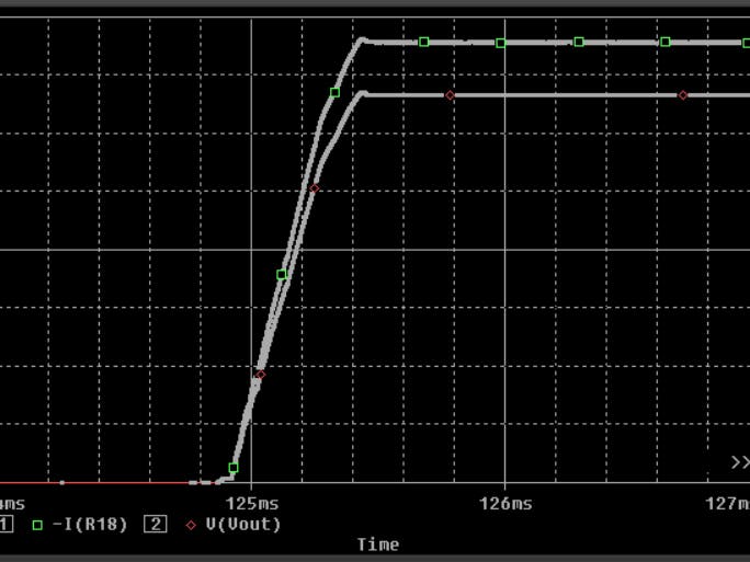
Note the value of C20, connected to the SS_TR node of the TPS54160, is 1 nF rather than the nominal value on the EVM of 0.1 uF. This change was made in order to shorten the startup time of the transient model, since we are interested in ripple rather than startup behavior and would like to shorten our simulation time. The startup behavior for the two values is compared below:
Figure 19: Startup Behavior for SS_TR capacitor value of 1 nF (top) versus the nominal 0.1 uF (bottom).
While both have a long delay in starting (126 ms), the slope of the startup is drastically steeper for the reduced SS_TR capacitance. As this is the point where the circuit behavior becomes more complex, the simulator slows down considerably, and thus the ~50 ms reduction in time to reach steady state cuts the simulation time from over an hour to roughly fifteen minutes.
To configure the simulation, create a new simulation profile from the PSpice menu, selecting the ‘Time Domain/Transient’ mode and configuring as follows:
While running stepped simulations with varying currents or parameter values would have been convenient, I found that it caused simulation failures and so ran each configuration separately. In order to speed up the simulation process, I modified the simulation speed to 5, set the RELTOL value to 0.003, and slightly loosened the absolute and voltage tolerance conditions in the options menu as shown:
Additionally, ensure that the transient.lib file is included in the config files for the project.
The steady state ripple for current and voltage appears as shown:
The setup in LTSpice is very similar, with the “.tran” command as well as the option configurations included on the schematic.
However, LTSpice’s solutions for this simulation ran prohibitively slowly, and as such only a small number of cases were simulated.
A block diagram of the experimental setup is included below:
The EVM provides test points at the input and output voltages that can be used to attach oscilloscope probes; a magnetic current meter can be connected to the wires leading to the electronic load.
In the lab, imprecision of instruments presented a significant obstacle to exact data collection; shown below is the baseline ripple in voltage and current with an open load:
Figure 20: Open Load Ripple for current (channel 3, blue) and voltage (channel 2, green).
Additionally, the power supply reached only 20 V of output, preventing the upper ranges of the EVMs input capacity from being evaluated.
DC Parameter SweepThe DC operating points for a range of input voltages and currents are charted (for a single configuration) below:
As suggested by the simulations, the output voltages are higher for lower current values, though it is difficult to differentiate between the values at different voltages or frequencies; this makes sense as the difference between frequencies in the simulated outputs was in the tens of microvolts. The bulk of the variation is between currents, suggesting that most of the loss is in conduction loss rather than switching loss, either in circuit components or in the measurement connections.
Additionally, the converter efficiency is tabulated for a range of circuit configurations at 1.5 A:
As discussed in the analysis of the simulated DC output in PSpice for TI, the converter efficiency is relatively uniform (roughly 80%) across most configurations. The exception to this was for cases with 10 uF of output capacitance and 250 kHz operating frequency, at which the efficiency dropped sharply. In order to determine the reasons for this, I moved to studying the ripple behavior of the circuit.
For a configuration not falling into the above category, the ripple appeared roughly as follows:
Figure 21: Output Ripple for 250 kHz, no extra input capacitance, 220 uF output, and 15 uH inductance. Note the approximately linear voltage ripple (green), with the current ripple (blue) fairly insignificant compared to the baseline.
The output current and voltage ripples, reduced by the baseline peak-to-peak instrument error reported above, are tabulated below in comparison with the values from the PSpice for TI simulations:
Table 2: Output Voltage and Current Ripple for 1.5 A Output Load, in millivolts and milliamps respectively.
Table 3: Output Voltage and Current Ripple for 0.75 A Output Load, in millivolts and milliamps respectively.
Even with the baseline variation subtracted, the experimental values are drastically different from the simulated values. However, the trends indicated by the simulations generally hold: the most drastic factor in voltage ripple is the output capacitors, then the frequency, then the inductor, with the input capacitors having minimal effects. For the output current ripple, the most important factor is also output capacitance, then frequency, but inductance plays a much more substantial role.
Now consider the major outliers discussed above, the 1.5 A trials with 10 uF output capacitors and 250 kHz frequency; referring to the efficiency table, we can see that both powers and the converter efficiency also drop significantly for these configurations. We can observe the output for one such configuration:
Figure 22: Output Ripple for no extra input capacitors, 10 uF output, 18 uH inductance, and 250 kHz. Note the switching behavior of the input voltage (yellow).
Observing the moments when the ripple is significantly larger, we can see that the switching behavior of the input voltage is also absent; this suggests that the diode does not stop conducting on these cycles, and the capacitor continues to discharge and the voltage (and average current) continue to drop. This behavior suggests that the 10 uF capacitor value is not appropriate for 250 kHz operation and high output load, as it does not adequately limit the voltage ripple for the longer period. The PSpice simulations do not indicate this possibility, but they do suggest that these configurations will have the largest ripple by far.
Notably, this behavior is not exhibited in the 0.75 A case, where ripple is generally smaller.
Conclusions and ComparisonsThis project indicates substantial variation between the real-world results of a buck converter circuit and simulated results. While some of this can be attributed to imperfections in measurement equipment, it is important to note that real world circuit operation will always contain non-idealities that are not modeled in simulation; also, simulators make significant approximations in order to compute solutions, which can create notable error in the results. However, the project also demonstrates that simulators accurately predict the pattern of behavior exhibited by real-world circuits and serve as a robust first test to catch circuit design errors early and to provide advice on component selection. These simulations accurately predicted the relatively large importance of the selection of the output capacitor and the converter frequency in the output ripple, and the converter’s ability to maintain the target output voltage for varying input voltages across most configurations, with the most significant factor in average output voltage being the load current. The simulator also allows a quick evaluation of otherwise difficult trials, such as a Bode analysis to prove that the converter is stable in response to noise in the output load.
In comparison with LTSpice, the PSpice for TI simulator generally produced similar numerical results. However, there were several notable divergences in the user experiences of the two tools. The most notable of these was the simulation time for the transient simulation. Where PSpice for TI was able to quickly simulate the very simple pre-startup behavior before slowing down during startup as the circuit began to switch, LTSpice maintained a much slower pace throughout the simulation, even with settings optimized for speed. This resulted in transient simulations that were anywhere from five to ten times as fast in PSpice for TI than in LTSpice.
Some other advantages of PSpice for TI that I have identified include the more detailed user interface, which hastens the process of developing and debugging simulations by making various simulation options immediately accessible without perusing documentation for the appropriate syntax. Moreover, the ability to save several simulation profiles in association with a schematic is extremely useful when conducting a large array of simulations on one circuit, allowing much more organization than the collection of SPICE commands required in LTSpice. PSpice for TI also allows a much more streamlined process for saving and reloading data output by simulations, allowing for an easy comparison across simulation runs where necessary.
There are a few areas in which the user experience of the tool could be improved: for example, PSpice for TI does not include a method to display labels or a legend for the different traces in a parameter sweep. Additionally, designs integrating any third-party model require at least one and no more than three markers to be placed on the schematic; the simulator sometimes requires these markers to be confirmed by the user on every run, even when the markers have not changed.


Comments