


Hardware components | ||||||
 |
| × | 1 | |||
 |
| × | 1 | |||
 |
| × | 1 | |||
 |
| × | 1 | |||
 |
| × | 1 | |||
Software apps and online services | ||||||
_4YUDWziWQ8.png?auto=compress%2Cformat&w=48&h=48&fit=fill&bg=ffffff) |
| |||||
This project tutorial is a good lesson on how to build a sensitive morning alarm system. This simple photosensitive alarm activates a buzzer when light shines directly on the connected LDR. The system should be placed on the window at night so that when the light appears in the morning, it will activate the buzzer to alarm. The alarm makes use of a buzzer which is powered by a 9V battery. Read through to understand more.
- Components:
- Battery 9V
- Photoresistor LDR
- BC547 Transistor
- Resistor 1k
- Buzzer
This circuit can be tested on the breadboard before making an order for the board prototyping. You can also simulate it through proteus EDA if you cannot find the components for use on the breadboard. The simulation is also a perfect way of testing the circuit before ordering for manufacturing.
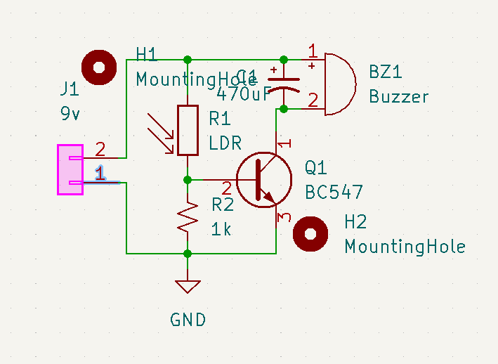
The Circuit Diagram.The components should be connected as shown in Figure one below:
The Circuit is similar to that of the automatic lighting circuit. But here the transistor is activated when the LDR is hit by light. The photoresistor and the connected resistor make up a voltage divider. To understand this circuit make sure you go on basic electronic knowledge of how a transistor works.
At night or when the system is placed in darkness, the LDR possesses very high resistance much higher than that of the connected resistor R1. This tells us that the voltage divider delivers very little voltage to the transistor base hence the transistor is not biased. The transistor remains off and thus the buzzer on the circuit remains deactivated.
When the LDR is supplied with enough light its resistance is reduced. This outputs a high voltage which is supplied to the base of the transistor in the circuit and thus it gets biased hence turning ON. The turning on of the transistor activates the buzzer and it beeps, alarming the user.
Connecting Circuit on the Breadboard for Testing and Prototyping.The circuit is connected to the breadboard as shown above.
PCB LayoutUsing KiCAD EDA, the circuit is converted into PCB, and the layout is prepared. The layout process will involve arranging the components, determining the size of the board, sizing the traces, adding filled zones, and generating the manufacturing files such as Gerber, drill, pick and place, and BOM. This is done nicely and the result is shown below.
PCB 3D Files Generation
From the PCB Layout, we can generate the 3D files as shown in the photos below:
This project is something that can be ordered instantly online and delivered within seven days from the comfort of your home anywhere in the world. Some of our readers keep wondering how this is possible. thanks to the worldwide PCB manufacturer PCBway for the good service they are offering. I have always trusted them when it comes to ordering such boards and they have never disappointed.
the process is very simple and you just need to create an account with them, then log in clicks on the instant order page, and order your board through the simplest p[rocedure placed on that site. it is simple, affordable, and deliverable.


_Ujn5WoVOOu.png?auto=compress%2Cformat&w=40&h=40&fit=fillmax&bg=fff&dpr=2)
Comments