


Hardware components | ||||||
_ztBMuBhMHo.jpg?auto=compress%2Cformat&w=48&h=48&fit=fill&bg=ffffff) |
| × | 1 | |||
 |
| × | 1 | |||
 |
| × | 1 | |||
 |
| × | 14 | |||
 |
| × | 14 | |||
 |
| × | 1 | |||
 |
| × | 1 | |||
 |
| × | 1 | |||
Software apps and online services | ||||||
 |
| |||||
This article is part 2 of two articles/sketches that roll dice. In the part 1 article a single die is configured to allow it to be randomly thrown with the results being represented by an arrangement of seven LEDs - the seven LEDs are laid out to represent the standard and traditional pip patterns of a single six faced/sided die. In the part 1 design the LEDs are directly connected to the microcontroller; in this part 2 article we extend the design such that we may add more dice by using serial-parallel input/output ICs (SIPOs) (eg 74HC595s) which reduces connections to the microcontroller radically (to just three, irrespective of the number of dice we configure in a single cascade of ICs).
If you have not read the 'Rolling the Dice part 1' article then it may be helpful to start there. However, it is not a prerequisite.
Differences Between the Part 1 and Part 2 DesignsIn the part 1 article and design the LEDs representing a throw of the die are directly connected to the microcontroller meaning that each of the seven LEDs required a digital I/O port to be assigned. This works very well and is a straight forward way in which to connect a single die. However, if we wish to scale up to two (or more) dice then this approach is not very practical - too many digital I/O ports would be needed.
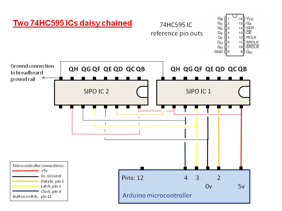
The part 2 design therefore introduces serial-parallel input/out ICs (SIPO ICs), eg the low cost 8-bit 74HC595 IC. This allows us to drive each of the eight IC's output ports using just three microcontroller connected wires. However, by cascading, or daisy chaining these ICs, we are able to drive 8, 16, 24, 32, 40,... output ports using these same three microcontroller connections - all of our LED connections can therefore be backed off to cascaded 74HC595 ICs with each LED being mapped to an IC output port. For convenience, we allocate one SIPO IC to each die so, for this design with two dice, we will be using 2 x 74HC595 ICs in a cascade (2 x 8-bit output ports). As we only require a maximum of seven output ports to map our LEDs to, this means that we end up with a spare and unused IC output port on each SIPO IC (port QA). However, the design caters for this.
The part 2 design accomplishes this by using the ez_SIPO8_lib library which provides easy to use functions to manage and drive these ICs singly or in cascaded form (we call these SIPO IC banks). For the part 2 design, we assemble two 74HC595 ICs into a single 2 x 8 port cascaded bank which allows us to assign each of our two dice to one IC and address their respective LED ports (die pip configurations) independently.
Whereas the part 1 design addresses the LED ports directly (ie using the function digitalWrite(LED,HIGH), etc), the part 2 design maps each die pip (LED) to a single addressable 74HC595 IC port by using the features of the ez_SIPO8_lib library.
The ez_SIPO8_lib works virtually, insofar as it allows us to assemble our output port configurations by software as bit mapped bytes (one byte for each die) and, when we are ready, transfer (xfer in SIPO8 library speak) these port/bit arrangements to the physical ICs in one process. The ez_SIPO8_lib library has many functions that allow us to update the IC's ports independently for each connected die, although for this design we will be using very few of its very rich and flexible features.
In the part 1 design, if we wish to address a specific pip we simply write a value (LOW/HIGH) to is allocated digital output pin number. However, in the part 2 design we cannot do this. Instead we need to address each pip (LED) by a bit address relative to its associated SIPO IC. The pip layout combinations for both dice for each face/side of a die are represented by a binary 8-bit byte pattern as follows:
- face/side 1, 1 pip :
0b00010000
- face/side 2, 2 pips:
0b01000100
- face/side 3, 3 pips:
0b00111000
- face/side 4, 4 pips:
0b10101010
- face/side 5, 5 pips:
0b10111010
- face/side 6, 6 pips:
0b11101110
So, for example, if we wish to send a pip value of two, then the associated IC's output ports would be bit 2 (port QC) and bit 6 (port QG) of each IC (we do not use output ports 0 (QA) in this design).
(Note that the RHS is the least significant bit and that the design does not use the QA port of the SIPO ICs (first output port), hence the least significant bit is always 0 in each pip pattern byte. Each of the above bit patterns provide the standard and tradition pip layout for each face of a six sided die when the associated LEDs are positioned as per schematics.)
Other than the above distinctions, the part 1 and part 2 sketch designs are largely the same and it will be seen that we also retain the same heart beat code as in the part 1 design.
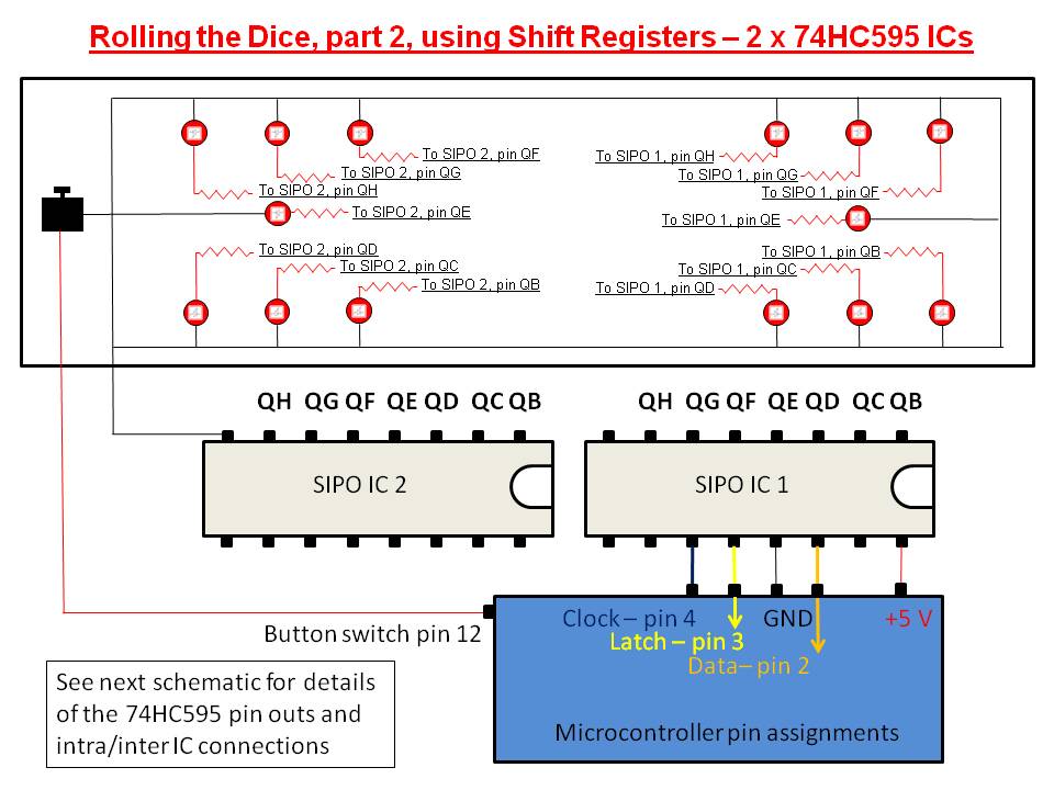
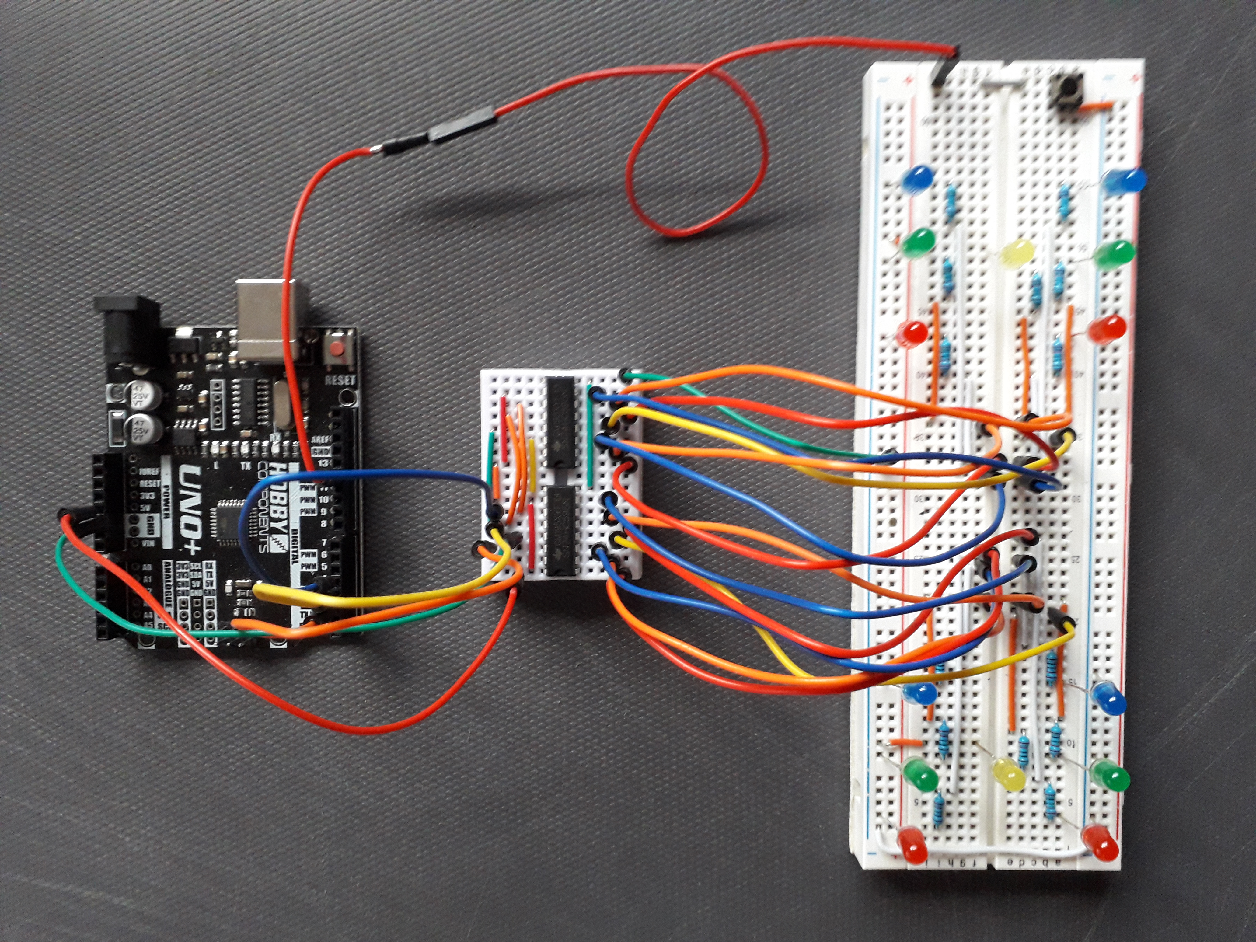
Hardware Design OverviewThe overall design is very much the same as the sketch offered in the part 1 article - a simply connected button switch is constantly scanned and, if switched, the dice are thrown with each die showing a random value of pips.
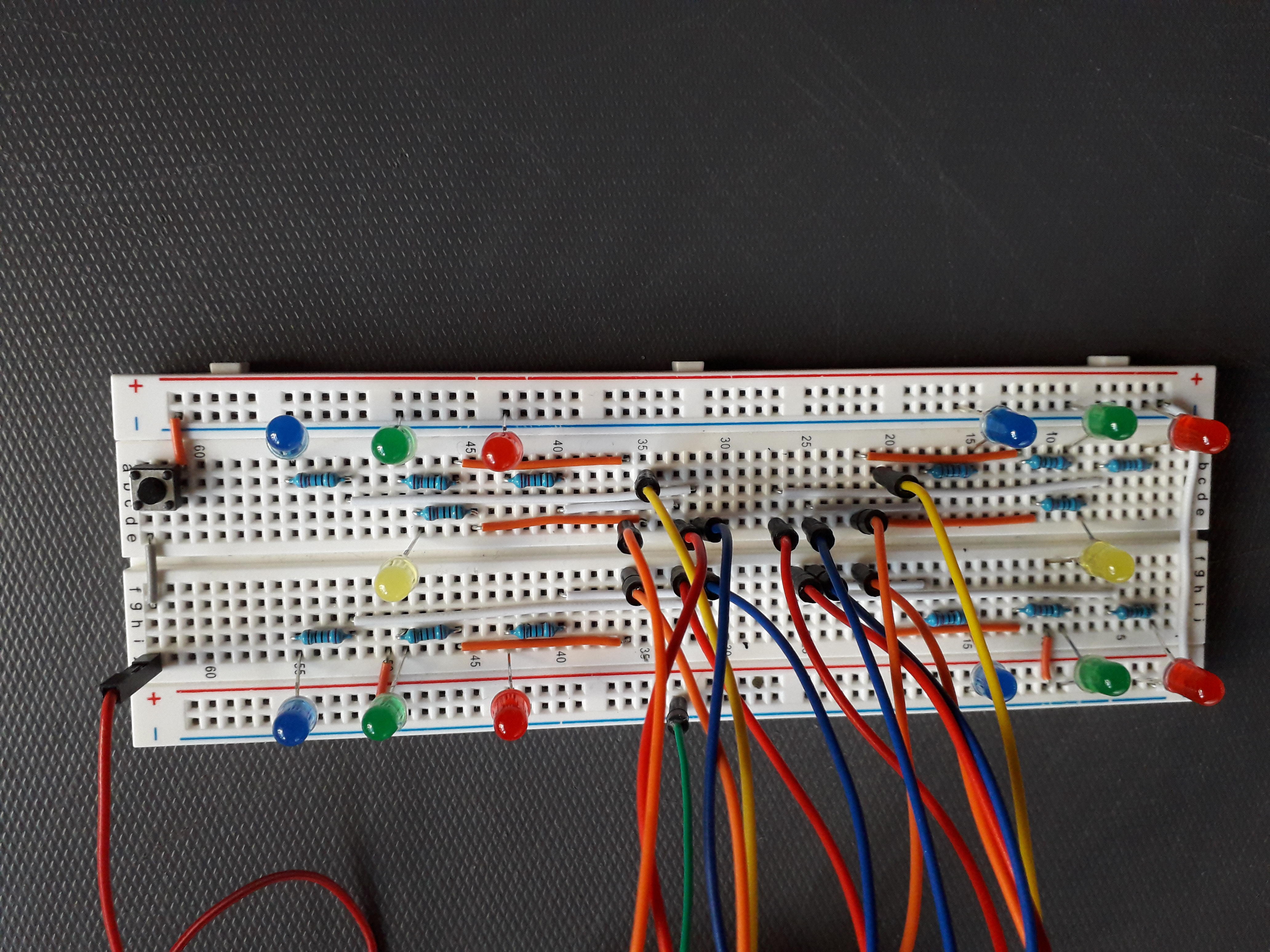
The same breadboard design and layout as in part 1 is maintained in part 2, albeit we now have seven LEDs representing each of the two dice on the breadboard. A simply connected button switch is again used to request a throw of the dice.
The schematics show the logical diagrams for the design. However, when dealing with serial-parallel input/output ICs we always seem to end up with a lot of wired connections. The logical schematics are therefore, in the main, drawn without these being shown. Instead, the wires connecting LEDs to the IC ports are labelled at each end to show how they are to be connected to each of the two ICs. For clarity, the two ICs are labelled 'SIPO IC1' and 'SIPO IC 2'. The output ports of each SIPO IC are labelled QB-QH so, for example, LED 4 of SIPO IC2 is labelled SIPO IC2 QE, etc. To note is that the design does not use port QA of either SIPO IC - the first LED of each IC is therefore reference as bit 1 of an 8-bit mapped byte as shown above.
Software Design OverviewAs mentioned above, the design and sketch makes use of two libraries, one for managing the button switch and the other for managing the SIPO ICs. To start, download these two libraries and their associated files as follows:
To incorporate the ez_switch_lib library, create a directory under your local Arduino/libraries directory called 'ez_switch_lib' and download the three files into this directory from the Project Hub article:
1. ez_switch_lib.h
2. ez_switch_lib.cpp
3. keywords.txt
To incorporate the ez_SIPO8_lib library, create a directory under your local Arduino/libraries directory called 'ez_SIPO8_lib' and download the three files into this directory from the Project Hub article:
1. ez_SIPO8_lib.h
2. ez_SIPO8_lib.cpp
3. keywords.txt
(Note that both libraries have extensive documentation and numerous examples in their application - User Guides, Crib Sheets, tutorials and sketch examples, if these libraries are of wider interest to you.)
Now let's look at the other principal parts of the sketch:
Library DeclarationandInitiation
Each of the two libraries used by the design must be declared and then initiated. The library declarations are straight forward enough, these being:
#include <ez_switch_lib.h>
#include <ez_SIPO8_lib.h>
Next we need to initiate each library instance and size for our purposes:
Switches my_switches(1);
Here we have sized the switch instance to be large enough for just one switch and will use 'my_switches' as its instance name. We do not define its type just yet (see setup).
SIPO8 my_SIPOs(num_dice, num_SIPO_timers);
In this instance definition for the SIPO library we will use 'my_SIPOs' as the name for the instance and include the following two parameters:
- a first parameter giving the number of physical SIPO ICs we wish to size the instance for - here we have designed our sketch for just two dice so '
num_dice' is defined as 2, one SIPO IC for each die (two SIPO ICs in total that we cascade - seesetup).
- a second parameter specifying the number of SIPO timers we wish to configure - the SIPO8 library also has a useful feature in that it can configure any number of timers. However, we do not use this feature in this sketch, although we could in the heart beat function if we wish. This value is therefore set to 0, that is
num_SIPO_timersis defined as 0.
Heart Beat Monitor
As in the part 1 design/sketch, I have included within the part 2 design/sketch the same heart beat monitor which is designed to flash the in-built microcontroller LED (LED_BUILTIN, usually on pin 13) at a frequency of 1 hertz (1 cycle per second). This provides some physical indication that the sketch is running (or not). If this aspect of the sketch is not required then it may be disabled by setting a macro definition in the heart beat declaration section to 'false'. That is, set '#define heart_beat_on false'. The associated data for the heart beat monitor is:
// Define heart beat data...
//
#define heart_beat_pin   LED_BUILTIN  // digital pin for heart beat LED
#define heart_beat_on    true         // determines if the implementation uses the heartbeat
long unsigned heart_beat_freq = 1000; // time(milliseconds) of heart beat frequency
long unsigned heart_beat_on_off_time; // the time the LED is on and off - 1/2 frequency
long unsigned last_heart_beat_time;   // time in milliseconds of last heart beat status change
bool heart_beat_status = HIGH;        // current status of heart beat, start high
//
I have already mentioned that the code uses the on-board LED (LEDBUILTIN) and how to disable the monitor if not required, but if you wish to vary the frequency of the monitor then edit the variable 'heart_beat_freq' to be the total number of cycles per second wished. Note that a complete cycle is on and then off, so the flash rate is automatically calculated to be 1/2 the selected frequency.
The heart_beat function is straight forward but the heart beat will only operate if the function is regularly called. It should therefore be called throughout the code, as can be seen in the sketch.
Now let's look at the other principal parts of the sketch:
setup - The setup function initialises everything needed by the sketch - the button switch (add_switch()), the SIPO cascaded bank (create_bank()) and the heart beat monitor. The two SIPO ICs are created as a single bank of two addressable 8-bit bytes (byte 0 for the first die and byte 1 for the second die) providing physical connectivity to the LEDs of each die, respectively. These are both explained below:
The add_switch() function has three parameters (switchtype, switch pin, circuit type), where
switch type- is defined by the library reserved macro 'button_switch',
switch pinis defined as 'button_switch_pin', the digital pin we have decided to use in our sketch, and
circuittype- this is defined by the library reserved macro 'circuit_C2'. This informs the switch library that the switch is to be wired simply without a 10k ohm pulldown resistor.
The returned value from the add_switch() call is the switch id which should be used in any functional call of the switch library.
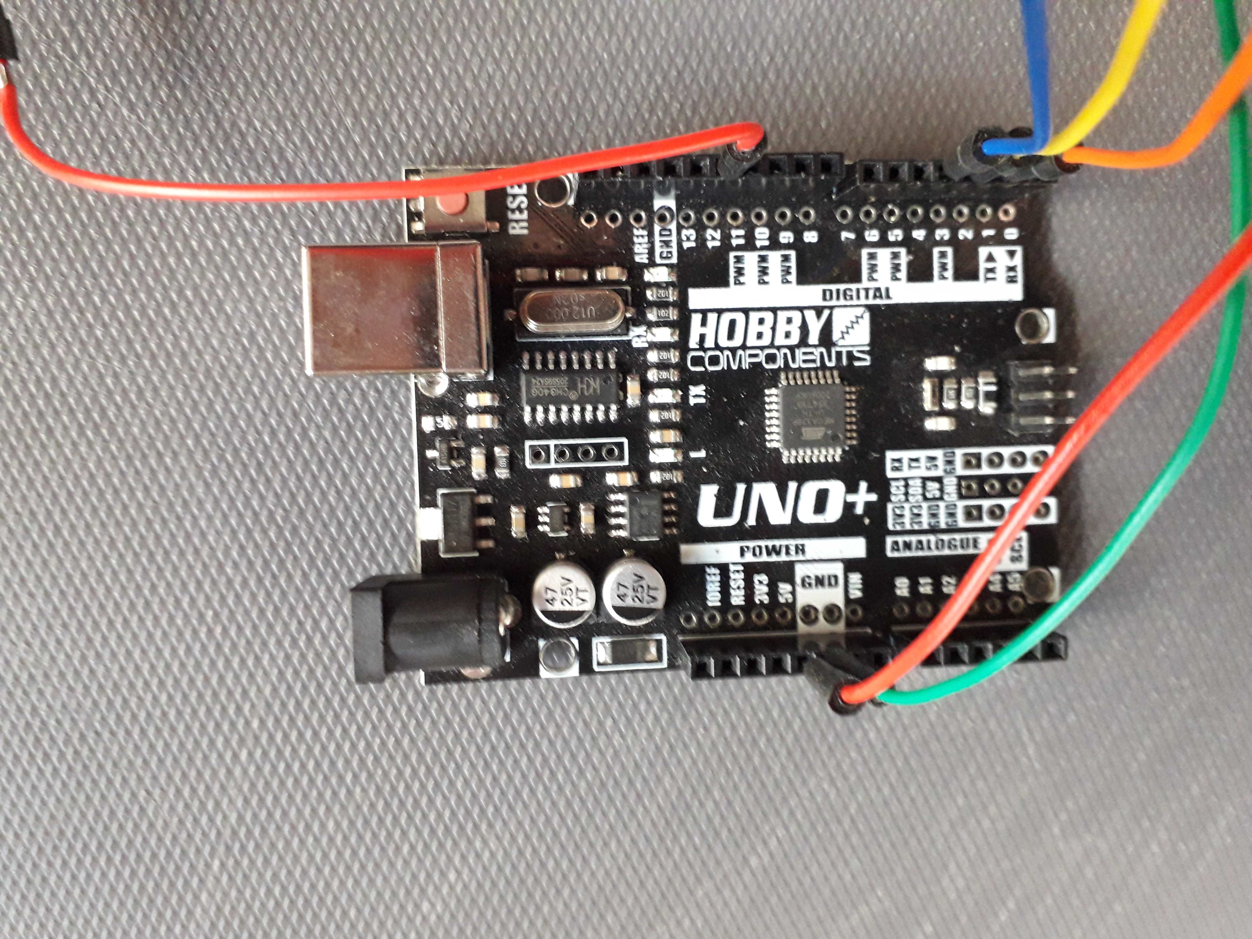
The create_bank() function has four parameters (data_pin, clock_pin, latch_pin, num_SIPOs), where
data_pinis the digital output pin assigned for the SIPO serial interface assigned by the sketch, here it is pin 2
clock_pinis the digital output pin assigned for clocking the SIPO and is assigned to pin 3 by our sketch
latch_pinis the digital output pin for triggering a latch of the the SIPO bank and is assigned by our sketch to pin 4, and
num_SIPOsdefines the physical number of 8-bit SIPO ICs we have cascaded in our SIPO bank, here 2
The returned value from the create_bank() call is the bank id which should be used in any functional call of the SIPO8 library.
To note is:
- the assignment process for the button switch and SIPOs are verified for success. If either cannot be assigned, for any reason, then the sketch will terminate. This will be seen if the heart beat monitor has been configured and it is observed not to be operating (flashing)
- the data, clock and latch pin values are only used in creating a SIPO bank - they are not referenced again thereafter even when we shift out data (
xferinez_SIPO8_libjargon) to the ICs.
clear_pips - this function clears all bits in each of the two dice and updates their physical SIPO IC ports (LEDs). The function uses two SIPO8 library functions, these being:
set_bank- this function resets every bit in the SIPO bank defined by thebank_idparameter. You do not need to know how many 8-bit SIPO comprise the bank as all will get reset to the parameter value specified, here LOW (0)
xfer_bank- the function transfers out all bits defined by the specifiedbank_idto the physical SIPO ICs (LEDs). In the design, we always assume that bit numbering is from right to left and so the final parameter of the function call is to shift out starting at the most significant bit (MSBFIRST). Again, we do not need to know how many SIPO ICs comprise the specified bank - this is automatically determined.
announce_throw - this function is called just before a throw of the dice to provide visible indication that the throw is about to start. The LED pattern is defined by five bytes with each bit position of each byte indicating which LED is to be illuminated (note we do not use bit 0 of each SIPO output port, QA). The preset data for the pattern is:
...
#define faces_per_die 6
#define die_1         0
#define die_2         1
...
#define num_patterns  5
 uint8_t announce_pattern[num_patterns] = {// simple strobe sequence - down and up
   0b00100010, // outer two top LEDs of a die
   0b01000100, // outer two middle LEDs of a die
   0b10001000, // outer two bottom LEDs of a die
   0b01000100, // outer two middle LEDs of a die
   0b00100010  // outer two top LEDs of a die
 };
The bit pattern can be anything, but the one coded provided a short strobe effect. Worth of note is that the function works with each die separately within the SIPO bank. It does this using the library function set_bank_SIPO, one call for each of the two die (SIPO ICs), as follows;
set_bank_SIPO- the function has three parameters - ourbank_id, the byte in the bank we wish to update (byte 0 for the first die and byte 1 for second), and the byte (bit pattern) to be written to the specified SIPO byte (die 0 or 1). For instance:
 // Start by clearing down the existing die pips/score
 clear_pips();
 for (uint8_t cycle = 1; cycle <= num_cycles; cycle++) {// do 'num_cycles' cycles
   // send each face/side strobe pattern to each die with a short delay between each
   for (uint8_t pattern = 0; pattern < num_patterns; pattern++) {
     my_SIPOs.set_bank_SIPO(bank_id, die_1, announce_pattern[pattern]); // set first die to this 'pattern'
     my_SIPOs.set_bank_SIPO(bank_id, die_2, announce_pattern[pattern]); // set second die to this 'pattern'
     my_SIPOs.xfer_bank(bank_id, MSBFIRST); // transfer (xfer) out the dice bits to the physical cascaded SIPOs
     delay(50);
     heart_beat(); // keep pumping the heart beat
     clear_pips();
   }
 }
throw the dice - The throw_dice() function firstly 'announces' that a throw of the die is about to start by cycling each of the seven LEDs for each die on/off over two cycles by calling the announce_throw() function. How this function 'announces' a throw is about to start is arbitrary and may be coded to display any pattern wished (see above).
After this, the function resets the random seed at each call and then determines a throw value (a random face/side of the die) in the range 0-5. Once a random face/side value is determined, the associated bit pattern for that die face/side is assembled using the function set_bank_SIPO which updates the virtual byte for the referenced die (0 or 1) ready for transfer to the SIPO ICs. Only when a random face/pip value has been determined for both dice are the SIPO ICs physically updated using the xfer_bank function. Because we defined our two SIPO ICs as a single bank comprising IC 0 and IC 1 the function knows to move out both pip value bytes for the dice cascade. Once this occurs, the dice then display the random face/pip value patterns following a press of the button switch.
 uint8_t die_face;
 die_face = random(1, 104640) % faces_per_die;   // range 0-(faces_per_die-1)
 my_SIPOs.set_bank_SIPO(bank_id,
                        die_1, // first die in the bank
                        pip_patterns[die_face]); // load first die pip patern for this face
 die_face = random(1, 104640) % faces_per_die;   // range 0-(faces_per_die-1)
 my_SIPOs.set_bank_SIPO(bank_id,
                        die_2, // second die in the bank
                        pip_patterns[die_face]); // load second die pip pattern for this face
 my_SIPOs.xfer_bank(bank_id, MSBFIRST);          // move dice data to the physical cascaded SIPOs
main loop - The main loop of the sketch is very simple and continually cycles checking the status of the simply connected button switch. Only if a press/release cycle is detected will a throw of the dice be actioned by calling the throw_dice() function:
void loop() {
 do {
   heart_beat(); // keep pumping the heart beat timer every cycle
   if (my_switches.read_switch(switch_id) == switched) {
     // Switch has been pressed and released, so throw the die...
     throw_dice();
   }
 } while (true);
}
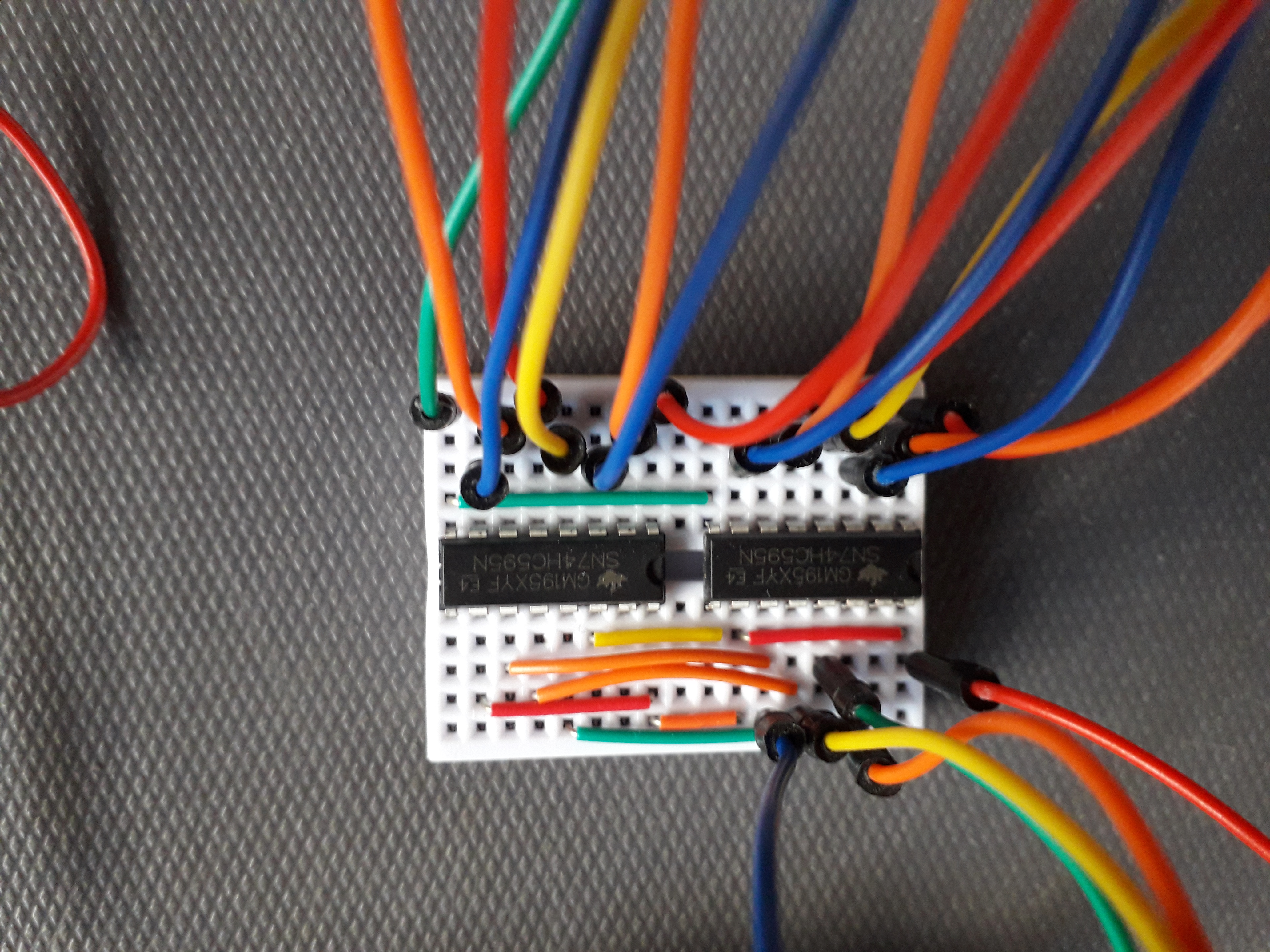
Without doubt the most difficult aspect of this article lies in the layout and wiring of the dice and the 74HC595 ICs. However, a little patience will be rewarded, so I hope you find the article of interest and fun.
If you have an interest or requirement for using serial-parallel input/output ICs (eg 74HC595 or others) then do have a look at the ez_SIPO8_liblibrary which provides many useful functions and techniques for managing and controlling these ICs, either singly or in multiple cascaded form arranged into banks. Indeed, these is no practical limit to how many may be cascaded into in a single bank or how many banks may be created, all of different sizes.
Breadboard layout with 74HC595 IC and microcontroller connections
74HC595 IC intra/inter connections


Comments