

Hardware components | ||||||
_ztBMuBhMHo.jpg?auto=compress%2Cformat&w=48&h=48&fit=fill&bg=ffffff) |
| × | 1 | |||
 |
| × | 1 | |||
Software apps and online services | ||||||
 |
| |||||
One of the most basic elements of the microcontroller (MCU) is the I/O – the number of pins, the sink and source strengths, and what features are available. In some cases, a mismatch may occur between the I/O needs of the system and the memory size of the microcontroller. Generally, the more I/O available, the more memory that is included, which makes the microcontroller more expensive.
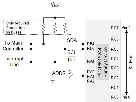
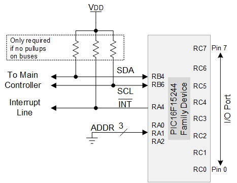
The I/O expander provides extra I/O bank(s) to the main microcontroller through serial communication, usually I2C or SPI. Common use cases of the I/O expander include simplifying PCB routing, improving power dissipation and physically shrinking the main microcontroller.
I/O expander ASICs are a common commodity, however each ASIC has slightly different features and use cases, which can cause headaches during design. However, I/O expanders are a relatively simple digital device that can be emulated using a microcontroller, such as the new PIC16F15244 family. This can yield more design flexibility, features, and even a lower Bill of Materials (BOM) cost than the associated ASIC based solutions. However, the ASIC based solutions have the upper hand in spatial and power efficiency due to the more specialized hardware.
To demonstrate the flexibility of this concept, we have created 2 separate code examples. The first code example is a very simple I/O expander. The firmware associated with this project could be easily tailored for even further simplicity in communication. The second code example is a very flexible “advanced” I/O expander, which was designed to allow practically every I/O setting to be controlled over I2C, rather than relying on pre-set features.
Both I/O expander examples share common features and much of the code base. Like many I2C devices, addressing lines are assigned to some of the unused I/O to set some of the bits for the I2C address, which provides flexibility in designs without extra programming. Unlike ASICs, these assignments can be changed, rerouted, removed, or reordered in software. Additionally, the device provides an external interrupt line (INT) to signal a change in the I/O level. INT can be either open-drain for a common line, or push-pull if this line is exclusive.
Simple I/O ExpanderBefore diving into the advanced I/O expander, let’s look at the simple one. There are two continuous states for each I/O line in this example (assuming the code is unmodified): a weak pulled-up input or an output LOW. The weak pull-up allows the I/O expander to define the logic level when used as an input and it also turns off connected circuits that would normally sink current into the expander. The strength of the internal weak pull-up in this device is on the order of 10s or 100s of µA.
The LOW output is a much stronger drive, with the ability to sink up-to 25mA per I/O, with a 300mA for the entire device (-40C to +85C). For more information on these limits, please see the electrical characteristics section of the device datasheet. One problem that could be encountered when transitioning from the output state to the input state is the charge time of the parasitic capacitance present on the I/O line. This capacitance can cause a delay in transitioning from 0 to 1, which may trigger the interrupt-on-change circuit. To minimize these effects, the simple I/O expander can be configured to momentarily switch on the high-side I/O driver to quickly recharge this capacitance before switching to the weak pull-up.
The run time for the high-side I/O driver is configurable in software and can be disabled, if desired. The images below show the enhancement to the rise time with this method – note the change in time scale from 20µs/div to 40ns/div in the images. Note: We do not recommend directly driving a capacitor in any configuration.
I2C communication with this example is also extremely simple. The complete I2C communication requires only 2 bytes for reads and writes. In an I2C write, the 1st byte of data is a bitmap which sets each I/O line, represented by a single bit, to an input or an output. All other bytes of data sent are discarded and can be omitted by the developer.
In an I2C read, the byte(s) read from the device are a bitmap that represents the digital value at each I/O line, which is accessed internally through the PORT register.
The objective when developing the Advanced I/O Expander was to provide a much more full-featured program than the simple variant shown above. The simple I/O expander has many limitations due to the extremely simple serial communication and is unable to leverage the menagerie of I/O-centric features available in the PIC16F15244 family, such as input level control, open drain outputs, maskable interrupt on change, and weak pull-up enables.
By contrast, this more complex example can configure almost every feature of the on-board I/O. To implement this feature set, the program uses a lookup table to determine which register to access or what function to execute. Figure 7 shows a sample application where the microcontroller acts a keypad controller, notifying the main microcontroller when a key has been pressed. (This example will be expanded on in a later post.)
Advanced I/O Expander – Program Structure
Figure 8 is the lookup table of “registers” in the device. Some registers in the table are physically present on every PIC16F15244 family device, such as TRIS and LAT, while other registers such as ERROR are “virtual.” The virtual registers are specific to this program and exist only in RAM.
One benefit of this lookup table structure is the flexibility to rearrange the registers, which can be used to optimize serial communications or to reduce the chance of a software glitch disturbing crucial settings.
The lookup table is split into two separate functions for reads and writes. This creates a simple and reliable permission scheme, at the cost of code size. For instance, to create a read only function, simply omit the address from the write lookup table.
Advanced I/O Expander – Communication
Communication with this example is more complex than the simple I/O expander. Before a read or a write can be performed, the controller must have indicated the address to start reading or writing to.
An I2C write uses the first data byte to set the address to start at. Then, the next byte is used to load data for that address. The address is then incremented for the next byte of data sent. This process can repeat so long as the address is still writable and valid, as shown below. If an invalid or read only address is written to, then the address is not incremented, and the device will not acknowledge (NACK) to signal that an error has occurred.
For I2C reads, the address to read from must be set first. Normally this accomplished with a single data byte written to the device, although some operations may set the address automatically for convenience. The I2C bus is stopped, then started again in read mode.
The 1st data byte of a read occurs at the address set. After this byte is read, the address is incremented, so the next read occurs at address + 1, address + 2 and so on. If an invalid or write only area is encountered, then the program stops incrementing the address and returns 0x00 until the read is stopped. Figure 12 shows a sample read of two registers.
This program stores 8 I/O related settings, all of which are documented in the device datasheet in more detail. The only I/O settings not saved are analog select (ANSEL) and PORT. It is assumed that the I/O expander is always digital, thus ANSEL is a constant value. The PORT value is the logic level present at the I/O bank, which is dependent on circuit conditions.
When referencing these registers, the “x” (e.g.: TRISx) refers to the selectable I/O bank that could be assigned. By default, bank C was used for this example.
- Tri-State Direction Control [TRISx] – Controls whether the line is an output (0) or an input (1).
- Latch [LATx] – Sets the output value of the I/O driver.
- Interrupt-On-Change Positive Edge [IOCxP] – Enables whether rising edges on the selected pins generate an interrupt.
- Interrupt-On-Change Negative Edge [IOCxN] – Enables whether falling edges on the selected pins generate an interrupt.
- Weak Pull-Up [WPUx] – Enables a weak pull-up for each selected I/O.
- Input Level Control [INLVLx] – Selects TTL or Schmitt Trigger CMOS input thresholds for each pin.
- Open Drain Control [ODCONx] – Enables open drain output functionality for the selected pins.
- Slew Rate Control [SLRCONx] – Enables slew rate restrictions to improve EMI performance on the selected pins.
Advanced I/O Expander – Memory Operations
As an additional feature, this code example supports the ability to restore default settings, save, load, or save and load its settings into internal non-volatile memory. The PIC16F15244 family does not have EEPROM, however a small section of Program Flash Memory (PFM) can be marked as non-executable by enabling Storage Area Flash (SAF).
Figure 13 shows how configurations are internally stored. Only a single memory row (32 words of 14-bits) is used to store the settings. This configuration simplifies the memory management and leaves the remaining non-executable memory free for other uses.
The I/O settings that are configurable are saved to the PFM, along with a simple (software-created) CRC-8 checksum to verify integrity of the configuration. To pack the CRC into the available space, it is split into chunks of 2 bits and attached to the first 4 settings of each configuration.
If the loaded configuration fails verification with its checksum, it is not loaded into the appropriate registers. For memory loads, the I/O pin behavior can be specified in the memory operation byte, shown in Figure 14. If the load fails, the pins will remain in that state until reconfigured.
The I/O settings can be saved and loaded to any of the four configurations at runtime. As a compile option, the developer or designer can set the device to try and load configuration 0 on startup rather than the defaults, which could be used as a simple firmware update that does not require a full reprogramming operation. If configuration 0 fails CRC verification, the program boots with the default I/O settings.
The default I/O settings on the device are defined as constants, which the developer can set as needed for the application. These defaults are not modified by the program and are considered a known good value. Running the memory operation “load defaults” will load the registers with these default values.
As a failsafe, all memory operations (excluding the load on startup) require a specific sequence of bytes to “unlock” the operation. This reduces the chance that a software glitch will erase or overwrite settings.
ConclusionAs shown in this article, simple 8-bit microcontrollers can be a reasonable substitute for a generic I/O expander ASIC in applications that require flexibility in I/O configurations or which utilize a cornucopia of I/O expanders in a single system. The required firmware for both examples is available on Github through the links below. Demo libraries and code for the Advanced I/O Expander, utilizing an Arduino Uno, are provided in the Github as well.
This is part 1 of a 3-part blog post series. The next post will cover utilizing the advanced I/O expander to control 7 segment displays.
For part 2 of this series, covering the use of the I/O Expander to control 7-segment displays, please see this Hackster Post.
For the final part of this series, covering the use of the I/O Expander to create a keypad controller, please see this Hackster post.


Comments