


Hardware components | ||||||
 |
| × | 1 | |||
| × | 1 | ||||
Software apps and online services | ||||||
 |
| |||||
This code example demonstrates the interfacing of PSoC 4200 pioneer kit with MB39C031-EVBSK-01 evaluation kit. The MB39C031 is the I2C configurable device, so the PSoC 4200 can be used as I2C master to configure the MB39C031 device.
Requirements:- Tool: PSoC Creator™ 4.0
- Programming Language: C ( ARM GCC 4.9.3 and MDK compilers)
- Associated Parts: PSoC 4200, MB39C031-EVBSK-01 evaluation kit
Related Hardware: CY8CKIT-042 pioneer kit, MB39C031-EVBSK-01 evaluation kit, DC-DC power supply, Multi meter
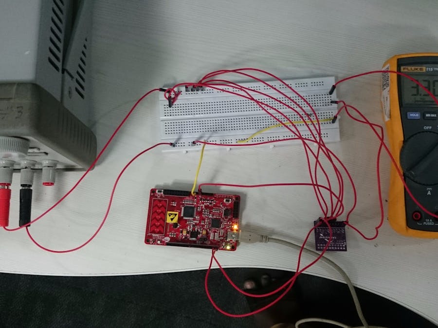
Hardware Connections:
1. To check the functionality of the MB39C031 device, it is required to do the following steps.
- The snap shot of the MB39C031-EVBSK-01 evaluation kit is attached here.
- The unregulated power supply is connected to the Vi terminal (which is marked in the snap shot). The Ground terminal of power supply, multi meter, MB39C031-EVBSK-01 evaluation kit and PSoC needs to be shorted.
- The below control terminals are available in the board.
§ CTL1 Control pin for 1st channel Buck DC/DC converter
§ CTL2 Control pin for 2nd channel Buck DC/DC converter
§ CTLL Control pin for LDO pin
§ CTLM Control pin for common block and digital block
To enable the particular channel or LDO, the CTLM and the appropriate CTLx pin should be high (It can be shorted to Vi terminal externally).
- Once the Vi and CTLx is supplied, the corresponding PGx should be high. If the device works fine, the PGx of the corresponding CTLx is high and ERR also will be high.
- The more information about the development kit is available in below link:
http://www.cypress.com/file/227276/download
I2C configuration:
The MB39C031 provides configurable output voltage based on the I2C data which is sent by I2C Master. The more information about I2C address and data is provided in below link, page no 31-41:
In the attached project, the 2 channels and LDO is controlled by PSoC 4200 device. The firmware is developed to control the MB39C031 device.
- Connect DC-DC supply to Vi input of the MB39C031-EVBSK-01 evaluation kit.
- Connect Vi to the CTLx of the required channel of MB39C031 which needs to be enabled. This connection should be done externally.
- Connect PSoC4200 VDD pin to VCCI2C pin of the MB39C031-EVBSK-01 evaluation kit.
- Make sure that Ground of DC-DC supply, PSoC4200 pioneer kit, Multi meter and MB39C031-EVBSK-01 evaluation kit are connected.
- The input voltage of the DC-DC supply can be set 2.5-5.5v. Here 4.0v is set for testing.
- In the project, there are below lines which is used to configure 2 channels or LDO in MB39C031 device.
The I2C address of the device is 0x2E. It is initialized as below.
#define I2C_SLAVE_ADDR (0x2Eu)
/* Buffer and packet size */
#define BUFFER_SIZE (2u)
#define PACKET_SIZE (BUFFER_SIZE)
There are two channels and LDO in the MB39C0321 device. The SOP_PACKET_CHx or SOP_PACKET_LDO is used to define the address of particular channel or LDO. Similarly, OUTPUT_VOLTAGE_CHx or OUTPUT_VOLTAGE_LDO mentions the output voltage of the particular channel or LDO.
/*Start of Packet for CH1 - It includes address of CH1 DC/DC converter and output voltage*/
#define SOP_PACKET_CH1 (0x00u)
#define OUTPUT_VOLTAGE_CH1 (0x03u) // 0x03 is equal to 1.06v
/*Start of Packet for CH2 - It includes address of CH2 DC/DC converter and output voltage*/
#define SOP_PACKET_CH2 (0x01u)
#define OUTPUT_VOLTAGE_CH2 (0x03u) // 0x03 is equal to 1.35v
/*Start of Packet for LDO - It includes address of LDO of DC/DC converter and output voltage*/
#define SOP_PACKET_LDO (0x02u)
#define OUTPUT_VOLTAGE_LDO (0x03u) // 0x03 is equal to 3.30v
/*Buffer for different channels*/
uint8 buffer_CH1[PACKET_SIZE]={SOP_PACKET_CH1,OUTPUT_VOLTAGE_CH1};
uint8 buffer_CH2[PACKET_SIZE]={SOP_PACKET_CH2,OUTPUT_VOLTAGE_CH2};
uint8 buffer_LDO[PACKET_SIZE]={SOP_PACKET_LDO,OUTPUT_VOLTAGE_LDO};
7. Once the project is built and programmed in the PSoC 4200 device, corresponding channel or LDO output can be measured using Multi meter. Here P4_0 and P4_1 is used as I2C pins and it should be connected with SCL and SDA of the MB39C031 device.


Comments