


This project documents my workflow for making a custom PCB with the xTool F1 Ultra using its fiber laser for direct copper removal.
One reason this machine is especially interesting for PCB experiments is that it combines two different laser sources in the same platform: a 20 W blue diode laser at about 450–455 nm and a 20 W fiber infrared laser at about 1064 nm. xTool presents the diode laser as the option for many common materials, while the fiber laser is the one intended for metal engraving, deep engraving, embossing, and thin metal cutting.
For this reason, I used the fiber laser for my PCB tests with xTool Studio 1.5.8. In this specific machine, it is the metal-oriented laser source, so it is the most natural starting point for experiments on copper-clad boards. At the same time, I do not want to oversimplify the physics: in the broader laser-processing literature, copper generally absorbs shorter visible wavelengths better than near-infrared light around 1064 nm. So I am not claiming that copper is easier to process only because of the infrared wavelength itself. In my case, the practical advantage comes from the fact that this machine’s fiber module is built for metal processing, and it was the one that gave the most useful copper-removal behavior during real PCB tests.
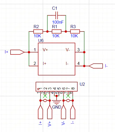
The board used in this test was a single-sided PCB (top layer only) made from 1 oz copper on 1.6 mm FR4, with 0.3 mm clearance and 0402 SMD footprints, making it a meaningful test case for fine-feature PCB prototyping.
The copper-clad board also needs to be properly sanded, cleaned and kept as flat as possible before engraving. Any oxidation, dirt, fingerprints, uneven sanding, or local warping can make copper removal less consistent and introduce unwanted defects.
My workflow can be divided into five main stages:
- Calibration
- PCB image generation
- Basic cleaning
- Focused cleaning
- Cutting
This work was inspired by previous xTool F1 Ultra PCB experiments shared online, especially a written article by Michael Parks and a practical YouTube walkthrough. My goal here is not to repeat those resources, but to document my own real workflow, including the specific adjustments that were necessary in my setup.
Before working on the actual PCB, I first performed the laser calibration procedure for the xTool F1 Ultra. According to the xTool workflow, this calibration is started from Device settings → Parameter settings → Fiber IR and blue-light laser calibration in xTool Studio.
For my setup, I used the black calibration sheet and followed the cross-alignment procedure. I designed or used the calibration pattern with two white crosses, then observed the variation between the blue and red light references on each cross. The goal of this step was to measure the offset between both laser references and correct it before processing the real PCB.
After completing the laser alignment calibration, I moved on to the actual PCB workflow: board preparation, image generation, focusing with AutoMeasure, copper removal and final cutting.
From the beginning, I always kept the PCB on top of that black metal plate to avoid damaging the original machine base. Since this process involves repeated engraving and cleanup passes, that support plate became an essential protective element in my setup.
Before measuring anything, I made sure the copper board was properly sanded and cleaned. I also checked that the surface was as flat as possible. This step matters a lot, because even small height differences can lead to non-uniform copper removal across the PCB.
For the distance measurement, I used AutoMeasure, but instead of measuring on the reflective copper side, I measured from the opposite side of the PCB, where the surface is less reflective. In my own tests, that gave me a more stable reference.
After that, I manually added +1 mm to the measured distance. This was not taken from a formal parameter table, it was simply the offset that gave me the best practical result after trial and error. There may still be another software or machine parameter affecting the effective focus behavior, but for now, this correction worked best in my setup.
2. PCB Image GenerationFor the PCB artwork, I first generated the board in EasyEDA and exported the visual result as a PDF/image in white on black. I used this format so that the black regions corresponded to the PCB clearance, meaning the copper areas intended to be cleaned by the laser, while the white regions preserved the trace and pad geometry.
After importing the image into the xTool software, the same black-and-white logic can also be obtained directly inside xTool Studio by using Adjust → Invert on the imported image.
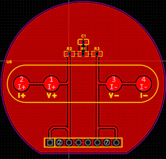
Because I was working from an image instead of directly from vector manufacturing data, scaling became a critical step. To make sure the imported geometry matched the real board dimensions, I used a known feature as reference. In this case, the PCB had a diameter of 44 mm, so I used that value for scaling.
At this stage, I also checked that the full board geometry stayed completely inside the machine working area. Since some practical laser-marking references and scan-field studies indicate that distortion and positional error can become more noticeable toward the edges of the field, I tried to place the PCB as close to the center of the working area as possible. This was a simple precaution to reduce potential alignment error during engraving.
Once the image was correctly scaled, I used the Trace tool inside the xTool software to convert the imported PCB image into workable paths. From this point on, this traced geometry became the actual working pattern for the rest of the process, so the original imported image was no longer needed.
After preparing the traced PCB geometry, the process moved to the first copper-removal stage, referred to here as basic cleaning.
The purpose of this stage was to remove most of the unwanted copper in a broader and more aggressive way, without focusing yet on the smallest details. A key setting here was Engrave → Advanced settings → Cross hatch, which helped the laser scan the area in both horizontal and vertical directions. In practice, this made the cleaning pattern more uniform and helped reduce the total laser exposure time needed to remove the bulk of the copper. Around 15 to 20 passes were required at this stage to achieve the desired level of general copper removal.
This stage was mainly intended to expose the general board pattern and separate the workflow into two goals: first, bulk copper removal; second, detail refinement. During this process, a useful visual cue could be observed: when the laser was still interacting with remaining copper, the emission appeared blue or sometimes blue-green in practice, while areas that had already reached the fiberglass substrate showed an orange appearance. The written PCB workflow that inspired these tests specifically describes remaining-copper spots as blue and fiberglass-reached areas as orange, which makes this color change a useful indicator during processing.
This stage used fewer passes and a higher frequency, specifically 40 kHz, following the general logic of the reference workflow used during the early tests. In practice, this step required around 10 passes to achieve the desired cleanup level. The goal here was no longer broad copper removal, but improvement of the isolation areas, edge definition, and smaller regions where residual copper was still present. xTool documentation for the F1 Ultra also notes operating ranges such as 30–60 kHz in relevant processing contexts, which is consistent with this kind of parameter adjustment.
5. CuttingIn my case, the PCB had a custom geometry, so I cut it in two steps: first a circle, and then a line. That sequence worked better for my design and gave me more control over the final result.
I treated cutting as a separate stage because a board can have an acceptable copper pattern and still fail mechanically if the final contour is inaccurate or badly aligned.
After the laser process was completed, the PCB was lightly sanded and cleaned again to remove residue and improve the final surface condition.
As a practical finishing step, I manually applied a layer of matte black spray paint to the PCB surface to help protect the copper against corrosion. This was used as a simple and low-cost alternative to a more formal UV protective coating or other dedicated finishing process.
After applying the black spray, the pads were carefully cleaned with tweezers to remove the paint from the unwanted areas and expose the copper only where electrical contact and soldering were needed. This step required patience, but it made it possible to preserve the protected surface while keeping the pads accessible for assembly.
At this stage, the workflow has only been tested on a single-sided top-layer PCB.
So far, I have not yet tested:
- drilling holes for through-hole components,
- adding a true silkscreen layer,
- applying a dedicated UV solder mask or a more standardized protective finishing process.
Because of that, this post should be understood as a validated workflow for copper removal, board shaping and basic post-processing, but not yet as a complete end-to-end PCB fabrication method.
AcknowledgmentsThis workflow was inspired in part by earlier PCB experiments shared by other makers working with the xTool F1 Ultra, especially Michael Parks’ written article and a hands-on YouTube walkthrough. My contribution here is the documentation of my own real test process, including image-based PCB scaling from EasyEDA, backside AutoMeasure, a +1 mm manual offset and a two-stage copper cleanup approach.
I would also like to thank the Laboratório de Sistemas Autônomos e Robótica Móvel (MOBI), CCT, Universidade do Estado de Santa Catarina (UDESC), Joinville, Santa Catarina, Brazil, for providing access to the equipment used in this project.
This project is connected to my master’s research in biomedical instrumentation at UDESC Joinville.

Comments