Hardware components | ||||||
_ztBMuBhMHo.jpg?auto=compress%2Cformat&w=48&h=48&fit=fill&bg=ffffff) |
| × | 1 | |||
 |
| × | 1 | |||
Assember programming is hardware level, we use a simple set of commands to perform mathematics and move bits around. At this level we turn circuits on and off with our commands.
Avrasm2 is the program from Atmel (now MicroChip) for their AVR products. You install it on Windows computers when you setup MicroChip Studio IDE or an older Atmel Studio Suite. The manual for AVRASM2 is online.
In this project I will be using the Avra assembler on Linux. We will use a text editor for our source file and the terminal window CLI. Do not use MSWord, WordPad or OpenOffice because these will add unseen formatting characters to the text.
Let's CodeWe are going to use this program, below. About once a second the sixth pin on PORTB of the microcontroller chip will toggle the Arduino Uno board LED on and off.
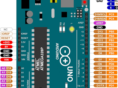
An image of the Arduino Uno is at the top of this project. Look for PB5 and you will find pin 13 at the right edge of the board. The Uno has an LED circuit built-in.
The bits from our program will be made into 0's and 1's that control voltages. We control which pins are output. PORTB is a block of 8 memory circuits located at address 0x25 and it outputs the binary value of the number PORTB. PINB is the input and sees the voltages at PORTB. DDRB is the Data Direction Register for PORTB at address 0x24.
This is a diagram of the circuits inside the microcontroller chip. PB0 is the first pin of PORTB and it is pin D8 on the Uno Board. PB5 has the built-in LED circuit connected. In the Arduino IDE we would turn on PB5 as an output with the command pinMode(LED_BUILTIN, OUTPUT).
When output pin PB5 to the Arduino Uno has DDRB = 1 then the output circuit for that pin is enabled. When DDRB = 0 then the circuit allows the pin to connect to register PINB and the voltage at the pin is an input.
PreparationDownload the blink.asm and m328pdef.inc files attached to this project. Create a new folder and put the two files into it.
Open blink.asm in a plain text editor like notepad.
Edit blink.asmAVR assembly language has a small number of commands. Words like inc, dec, clr or ldi mean things to the assembler program so we can only use them as the increment command, decrement, load immediate etc.
We are using DDRB and PORTB in our program, where do these words come from and what do they mean? They are not part of the Assembly language.
Assembly language allows us to substitute equivalent values. A text file called a definition file exists for the Atmega328p used in the Arduino Uno, a slightly different definition file has been created for the Atmega8 chip.
The definitions file for our exercise is attached. Open it with text editor and search for DDRB and PORTB. You find commands saying that one thing is the equivalent to another. For example, look for PB5 and you see:
.equ PB5 = 5 ; For compatibilityWhat this line means to the assembler is that when it sees PB5 in the program to use the number 5. We will come back to this in our project.
Registers
r0 to r31 are internal registers close to the processor heart. Each is an 8bit storage circuit where the controller we can perform mathematical operations. You can think of them as 8bit abacuses with bits in place of beads
Next we define some words, labels to help us remember and understand the code, to make it more logical to us. r16 is called mask and holds a value we will use it once to turn on the thirteenth pin on the Atmel MCU device.
r17 controls if the LED is on or off so we give it the name ledR. r18, r24 and r25 hold numbers that will count down to create a delay. We are giving the registers names in our program so that we puny humans can more easily understand our code.
Loop Values
The numbers used for the delay are named oVal and iVal when the assembler sees these names used in our assembly code it will use the locations of the assigned numbers.
Wait! 8bit numbers only go up to 255. How can we do math with numbers higher than that?
The AVR is able to work with numbers that have 16bits. We can count, multiply, divide numbers as high as 65025. We will see the special reserved keywords HIGH and LOW, later in the program that signal to implement the 16bit mathematics.
oVal is decimal 71 and iVal is decimal 28168. So the delay values are:
.equ    oVal    = 71        ; outer loop value
.equ    iVal    = 28168     ; inner loop value
We want the Arduino to use about a second to count down to zero. Do a google search for AVR Assembly and these numbers. You will find detailed calculations how long it takes for the commands to execute.
        clr    ledR
        ldi    mask, 0x20
        out    DDRB, mask
First, we clear ledR. We have told the assembler that ledR is just a name for r17 so we are really setting r17 to all zeroes. Outputting this value into the device register PORTB turns the LED off on the Arduino board.
Mask is our name for r16. We output the value to DDRB to set the Data Direction Register for for PORTB to input or output. out DDRB, 0xFF sets all 8 pins to output. Change the line to ldi mask,0x20, or 0b00100000 and now we are only turning on the sixth pin of PORTB.
A moment to think about Uno digital Pin 13 in the Arduino IDE. It really is the sixth pin of PORTB. Since we start counting at number 0, 1, 2.. 5 is actually the sixth number. How about we do some Arduino math and left shift a 1 in the ones position 5 positions to the left?
; shift a 1 five positions to the left
    clr    ledR
    ldi    mask, (1<<PB5)
    out    DDRB, mask
It works because the m328pdef.inc file says that PB5 is equivalent to the number 5. 1 << 5 means the one in our command is moved 5 positions and 0b00000001 becomes 0b00100000 which we write 0x20 in hexadecimal.
StartThe word start is just a label and we could call it anything. But using a word means we can understand better what we are looking at and we make a loop by ending the program with rjmp start.
start:
    eor    ledR, mask
    out    PORTB, ledR
In count.asm we output to PORTB the value we have labelled ledR which is stored in register r17. Then we increment ledR and continue with the program. In blink.asm we toggle the value in r17 that we have named ledR from 0b00000000 to 0b11111111.
The loopIt takes numbers and decrements them until they get to zero. When the value hits zero then the processor jumps out of the loop to its next command.
Let's take a look at how the loops work.
        ldi	oLoopR,oVal	    ; initialize outer loop count
oLoop:
        ldi	iLoopRl,LOW(iVal)  ; intialize inner loop LOW
        ldi	iLoopRh,HIGH(iVal) ; intialize inner loop HIGH
iLoop:
        sbiw	iLoopRl,1   ; decrement inner loop registers
        brne	iLoop	    ; branch to iLoop if iLoop not 0
        dec	oLoopR	    ; decrement outer loop register
        brne	oLoop	    ; branch to oLoop if outer loop not 0
        rjmp	start	    ; jump back to start
We enter the loops with oVal and iVal at their starting valuesin registers r18(oVal) and r24 and r25 splits the value for iVal. For each count of oVal the sixteen bit value iVal is counted down to zero. When the loops are finished the program returns to the location labelled start.
AssemblyTo generate an output hex file we have lots of options. On a Windows PC we can edit the assembly code with MicroChip Studio, MPLabX, CodeBlocks and assemble with the Avrasm2 installed with MicroChip Studio.
For this project let us use Avra compiler on Linux. Open a terminal in the directory where we have our.asm file and the m328pdef.inc definitions file.
Type
$ avra blink.asmIf all goes well we will see the following display
In the folder with the assembly source program we should see some new files that were generated as part of the assembly process. We are looking for the file blink.hex. Extra files will not affect our project.
Connect an Arduino Uno and check the port assigned. Open a terminal in the directory and enter:
$ avrdude -p atmega328p -c arduino -P /dev/ttyACM0 -U flash:w:count.hex:iAvrdude will take the hex file and upload it to the Arduino on port ttyACM0. Transmit and receive lamps will flicker on the board and the screen will show:
The LED built into the Uno board should now be blinking about once a second.


Comments