


Hardware components | ||||||
| × | 9 | ||||
| × | 2 | ||||
| × | 4 | ||||
| × | 1 | ||||
| × | 1 | ||||
| × | 1 | ||||
| × | 8 | ||||
| × | 2 | ||||
| × | 2 | ||||
| × | 5 | ||||
| × | 1 | ||||
Hand tools and fabrication machines | ||||||
 |
| |||||
 |
| |||||
This is my version of the LumiTrap by gokux. Gokux describes this as follows:
Seeking a non-toxic and sustainable method to rіd your space of insects? This solar-powered bug trap presents an eco-conscious alternative, removing the necessity for chemicals or pesticides, thereby ensuring safety for individuals and the environment. Whether safeguarding a vegetable gаrden from destructive pests or aiming to relish еvenings on your balcony or at a campsite free frоm insect swarms, this device serves as an optіmal solution. It is especially effective at capturing mosquitoes as well.
Check out Gokux's build on Instructables.
Parts & ChangesThe original LumiTrap was designed to be used outdoors where-as this build is for indoor use only. Power is provided from a 12V adaptor rather than from solar panels. When indoors, fan noise can become an issue. So circuitry has been added to allow control over the fan speed and UV light intensity.
This build increases the UV lamp power with nine 3W 365nm LEDs so as to attract more annoying bugs. The case was designed around a 100mm x 100mm x 18mm Aluminum Heatsink. The nine LEDs are glued on using thermal paste (you can get this from sites like Ali-Express).
The fan is a 92mm x 92mm x 25mm to fit in the case. Power and fan wiring is passed from the bottom section to the top section via 60mm M3 hexagonal brass pillars.
I printed this in ABS so it can withstand any direct sunlight. (PLA can weaken under direct sunlight).
UV Bug Trap - Top.stl - 0.2mm layer height with supports
UV Bug Trap - Fan.stl - 0.2mm layer height with supports
UV Bug Trap - Collector.stl - 0.2mm layer height without supports
UV Bug Trap - Post.stl - 0.2mm layer height with raft (clone to get 4 posts)
UV Bug Trap - Knobs.stl - 0.2mm layer height. Change to contrasting color at the start of layer 66.
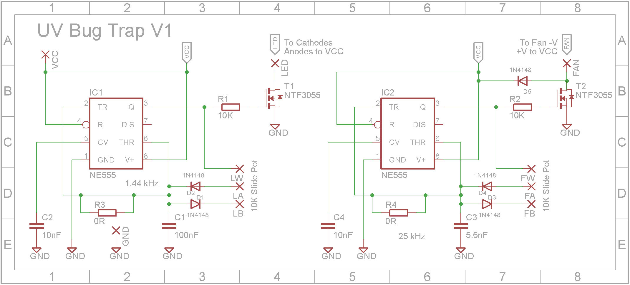
The schematicThe circuit design incorporates two PWM controllers. One controls the light intensity and the other controls the fan speed. The controller is designed around the 555 timer IC.
555 Trigger Pin
Pin 2 is the trigger pin. The trigger sets the output pin (pin 3) high when the voltage on pin 2 drops to below 1/3 of the supply voltage.
555 Threshold Pin
Pin 6 is the threshold pin. The threshold sets the output pin (pin 3) low when the voltage on pin 6 reaches 2/3 of the supply voltage.
Astable operation
When the 555 timer IC is configured in astable mode, capacitor C1 charges through resistors R1 and R2. While the capacitor is charging, the output is high. When the voltage across C1 reaches 2/3 of the supply voltage C1 discharges through resistor R2 and the output goes low. When the voltage across C1 drops below 1/3 of the supply voltage C1 resumes charging, the output goes high again and the cycle repeats.
Note that the on-time is determined by R1, R2 and C1 where-as the off-time is determined by R2 and C1. This means the on/off time can never be the same when the 555 timer is configured in this arrangement.
One method to make an equal on/off time is to add a pair on diodes.
By adding two diodes, charge time is determined by R1 & C1 and discharge time is determined by R2 & C1. By making R1 = R2, the on and off times are the same.
Pulse-width modulationThe following is an extract from ScienceDirect.
Pulse-width modulation is a digital technique to control a signal by repeatedly toggling a signal between a HIGH and a LOW state in a consistent pattern. We can portray new information by changing how long the signal is HIGH versus LOW. The PWM signal has two key parameters - frequency and duty cycle.
The period of the PWM signal(measured in seconds) indicates the amount of time it takes for the signal to complete one cycle. Refer to the image above. We can see that a period is a complete cycle of the signal, changing from LOW signal to a HIGH signal and back to a LOW signal. The signal pattern of each period is repeated over and over again.
The frequency of the PWM signal, measured in Hertz (Hz), indicates the number of complete periods that occur in 1 second. In our LaunchPad, the PWM signal typically has a frequency of 490 Hz. This means that our PWM signal completes 490 periods every second. The period and frequency of a signal are closely related, in that the faster the frequency, the smaller the period. The slower the frequency, the larger the period.
The relationship between period and frequency is realized with this equation:
For example, the period of a 1-kHz (1000 Hz) signal is 1/(1000 Hz) = 0.001 s or 1 ms.
The Duty Cycle of the PWM signal is the percentage of time that our PWM signal is in a HIGH state versus a LOW state. For example, a simple square wave has a duty cycle of 50%. However, we can change the duty cycle of our PWM signal, anywhere from 0% (for always OFF) to 100% (for always ON) and anywhere in between, depending on what type of information we want to portray.
PWM can also be used to control the power that is fed into certain electrical devices. By changing the duty cycle of a PWM signal, we can actually simulate an average voltage (or current) output. The longer the duty cycle is, relative to the period, means that, on average, the signal is more HIGH than LOW. This means on average more voltage (or current) is seen at the digital output pin. If we start at a duty cycle of 0%, we should see an effective average voltage of 0 V. Increasing duty cycle to 50%, we’ll start to see an effective average voltage of VCC/2. And lastly, at a duty cycle of 100%, we should see an effective voltage of VCC.
Fixing the frequency and varying the duty cycleWe saw how the 555 timer can change the on/off time (duty cycle) by changing R1 and R2. By using two diodes, the mark/space ratio is determined by R1/R2. The frequency will be determined by R1 + R2 and C1, that is the frequency is:
1 / (on time + off time)
Now replacing R1 and R2 with a variable resistor, we can change the duty cycle without changing the underlying frequency.
The above diagram shows two variants that essentially perform the same function. In the second variant, when the output is high, the charge path is pin 3, 2-3 of R1_R2, D2, C1 to gnd and when the output is low, the discharge path is C1, D1, 1-2 of R1_R2 to pin 3. I used this variant in this project.
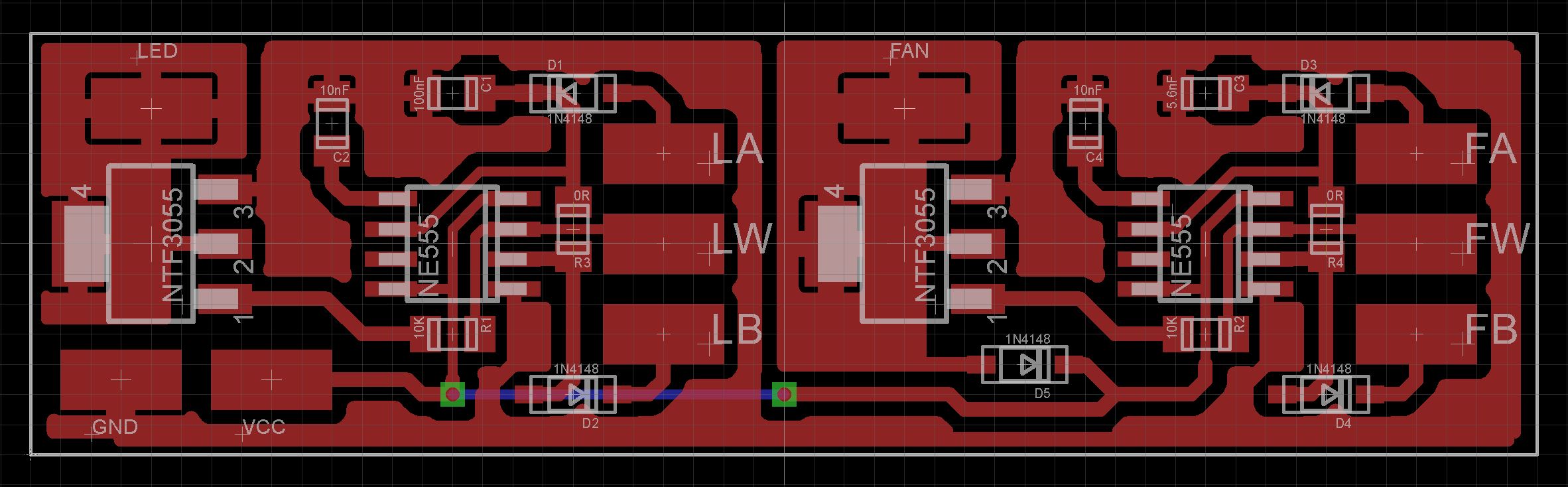
Assembling the PCBStart by adding the SMD components. I find it easier to use solder paste rather than use solder from a reel when soldering SMD components. I used my SMD Hot Plate to reflow the solder paste.
Add the links if your board is single sided.
Drill out the heatsink holes with a 2.5mm drill and create a thread with a M3 tap.
Arrange the LEDs in a 3x3 grid in the center of the heatsink. Make sure each is orientated correctly as shown in the photo below.
Glue in place using thermal paste. Leave the paste to dry for at least 24 hours.
Wire up with tinned copper wire as shown in the above photo. Note each vertical column is wired in series and the three columns are connected in parallel.
Assembling the bottom sectionSolder +12V and GND wires to the DC panel socket. Screw into base using M2 6mm screws.
Insert the fan using 45mm M3 screws which are screwed into the 60mm brass pillars. Use a spring washer, plain washer, eye terminal and another washer before placing the screw through the fan and case holes and into the brass pillar.
Once all screws are in place, cut the fan and power cables to length. See the photo below to see which eye terminals that they attach to. Remove each screw in turn and crimp/solder the wire to the eye terminal before screwing them back in. Note: both the Fan+ and +12V wires go to the same eye terminal.
Start by connecting three wires to each slider potentiometer. Screw them in to the top using 4mm M2 countersunk (flat head) screws.
Place the PCB in the top as shown in the photo below.
Cut and solder the wires from the slider potentiometers to the corresponding pads on the PCB.
Add two wires on the eye terminal that is screwed onto the +12V post coming up from the base. One wire goes to the VCC pad on the PCB and the other goes through a hole that connects to the anodes (+) of the LED columns.
Add one wire on the eye terminal that is screwed onto the GND post coming up from the base. This will go to the GND pad on the PCB.
Add one wire on the eye terminal that is screwed onto the FAN - post coming up from the base. This will go to the FAN pad on the PCB.
Solder a wire to the LED pad on the PCB and feed it through the hole that lines up with the LED cathodes (-) of the LED columns.
Slide on the four 3D printed posts and screw the top to the pillars using M3 x 8mm screws. Due to space limitations near the slider potentiometers, leave off the spring washer and plain washer when screwing in those two screws.
Cut the wires to the LEDs such that they will allow the heatsink to fold down when accessing the internal circuitry. Solder them onto the LED array.
Place the heatsink into the top and secure with four M3 6mm countersunk (flat head) screws.
Push any access wiring to the LED array back through their corresponding holes.
Applying PowerThe LEDs have a 3.2V drop and when three are mounted in series, the voltage should not exceed 9.6V. This is an average voltage so when using PWM, the voltage can exceed this provided the on time of the PWM signal is not excessively long. Start with the pots in the middle (you may have the A and B ends swapped so what you may think is minimum is actually maximum). Adjust the fan slider first to check are wired correctly. When using the unit don't have the LED slider exceed the halfway mark.
In the container section that slides in under the bottom section, add some oil, like coconut oil, to it. Make sure it is spread evenly. Slide the on the tray and place it somewhere it is dark and not too close to any light source.
ConclusionThe aluminium heatsink and 3W UV LEDs are really an overkill. I do like the industrial look with the massive heatsink. All in all, an interesting project. It is winter here in Sydney so the mosquitoes aren't around but come summer I hope to have a peaceful nights sleep without the annoying buzz of a mosquito near my head.
Thank you Gokux for an inspiring project 👍👍👍.


Comments