



Hardware components | ||||||
 |
| × | 1 | |||
Software apps and online services | ||||||
 |
| |||||
 |
| |||||
Hand tools and fabrication machines | ||||||
 |
| |||||
Introduction: Generating a Pulse Width Modulation (PWM) signal is one of the most fundamental requirements in embedded systems—whether you are driving servos, dimming LEDs, or controlling motor drivers. While high-level abstraction layers (like HAL or Arduino) can get a PWM signal up in a single line of code, they obscure the underlying silicon logic.
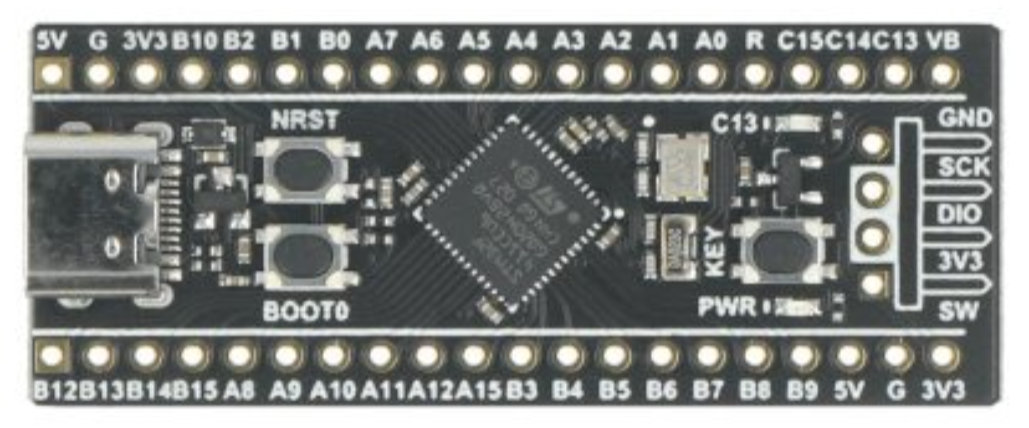
In this project, we are throwing away the libraries and configuring a general-purpose timer on the STM32F411CEU6 "Black Pill" from scratch using pure C and bare-metal register manipulation (CMSIS). We will configure TIM3 to drive two independent hardware PWM outputs on PB4 and PB5 simultaneously, completely bypassing the CPU once initialized.
How It Works: The Silicon Layer A hardware timer is essentially an autonomous high-speed digital counter. It uses the MCU's internal clock source (in this case, the default 16 MHz internal High-Speed oscillator, or HSI) and runs silently in the background.
The architecture relies on three primary 16-bit registers working in tandem:
Prescaler (PSC): Divides the incoming 16 MHz clock down to a manageable frequency. For a 1 MHz timer tick, we divide by 16 (PSC = 15).
- Prescaler (PSC): Divides the incoming 16 MHz clock down to a manageable frequency. For a 1 MHz timer tick, we divide by 16 (PSC = 15).
Auto-Reload Register (ARR): The ceiling value. The counter (CNT) ticks up until it matches ARR, then instantly resets to 0. This governs the PWM Frequency.
- Auto-Reload Register (ARR): The ceiling value. The counter (CNT) ticks up until it matches ARR, then instantly resets to 0. This governs the PWM Frequency.
Capture/Compare Register (CCR): The threshold value. A hardware comparator checks if CNT is less than CCR. This governs the PWM Duty Cycle.
- Capture/Compare Register (CCR): The threshold value. A hardware comparator checks if CNT is less than CCR. This governs the PWM Duty Cycle.
The Mechanism (PWM Mode 1):
While CNT is less than CCR: The physical pin is pulled HIGH.
- While CNT is less than CCR: The physical pin is pulled HIGH.
The moment CNT is greater than or equal to CCR: The pin drops LOW.
- The moment CNT is greater than or equal to CCR: The pin drops LOW.
When CNT reaches ARR: The counter resets to 0, and the pin pulls HIGH again.
- When CNT reaches ARR: The counter resets to 0, and the pin pulls HIGH again.
Step-by-Step Configuration Flow: Configuring bare-metal peripherals requires a strict order of operations across three layers: RCC (Clocks), GPIO (Routing), and the Timer Peripherals.
Layer 1: Powering the Blocks (RCC) By default, peripherals are clock-gated off to conserve power. A peripheral without a clock is completely unresponsive—writing to its registers does absolutely nothing. We must enable the clock for GPIOB on the AHB1 bus and TIM3 on the APB1 bus.
Layer 2: Routing Pins via Alternate Functions For a pin to carry a hardware-generated PWM signal, it must be detached from the standard CPU input/output register and handed over to the timer mux.
Set the pin mode to Alternate Function (0b10) in MODER.
- Set the pin mode to Alternate Function (0b10) in MODER.
Map the pin to AF2 in the Alternate Function Low Register (AFRL), which explicitly wires PB4 to TIM3_CH1 and PB5 to TIM3_CH2 in silicon.
- Map the pin to AF2 in the Alternate Function Low Register (AFRL), which explicitly wires PB4 to TIM3_CH1 and PB5 to TIM3_CH2 in silicon.
Layer 3: Timer Setup & Preload Buffers We calculate our registers using the standard formulas:
Frequency = input_clock / ((PSC + 1) * (ARR + 1))
- Frequency = input_clock / ((PSC + 1) * (ARR + 1))
CCR = duty_fraction * (ARR + 1)
- CCR = duty_fraction * (ARR + 1)
Crucially, we enable the Output Compare Preload bit (OCxPE). This acts as a vital safety buffer: when you update a duty cycle in your application loop, the hardware intercepts the write and waits until the current counting cycle completes before applying it, completely eliminating mid-cycle waveform glitches.
Common Gotchas & Troubleshooting:
No output on the pins? Ensure you enabled RCC->AHB1ENR and RCC->APB1ENR before touching any peripheral registers.
- No output on the pins? Ensure you enabled RCC->AHB1ENR and RCC->APB1ENR before touching any peripheral registers.
Using TIM1 instead of TIM3? Advanced timers like TIM1 require you to explicitly set the Main Output Enable (MOE) bit in the TIM1_BDTR register, or the pins will stay completely dead.
- Using TIM1 instead of TIM3? Advanced timers like TIM1 require you to explicitly set the Main Output Enable (MOE) bit in the TIM1_BDTR register, or the pins will stay completely dead.
Overwriting channels? When configuring channel properties in CCMR1, always use read-modify-write bitwise operations (|=). A raw assignment (=) to configure Channel 2 will silently wipe out your settings for Channel 1.
- Overwriting channels? When configuring channel properties in CCMR1, always use read-modify-write bitwise operations (|=). A raw assignment (=) to configure Channel 2 will silently wipe out your settings for Channel 1.


Comments