

Hardware components | ||||||
 |
| × | 1 | |||
 |
| × | 1 | |||
Software apps and online services | ||||||
| ||||||
 |
| |||||
 |
| |||||
In this project, we provide Maker's nRF54L15 Debug Board.
The nRF54L15 has just been released. Although Nordic official boards exist, makers are looking for something more useful.
We design and built a compact evaluation board (EVM) featuring the powerful nRF54L15 Wireless SOC.
The schematics designed in Autodesk Fusion, along with a BOM ready for immediate order from PCBWay, are also available.
These resources make it easy for Makers and new developers working with the nRF54L15 to get started.
This project is aimed for Makers, and those interested in exploring Nordic Semiconductor nRF54L Series.
You can download the Autodesk Project file(.f3z), Schematics(.pdf), Gerber(.zip) and BOM(.xlsx) files in the 'Schematics' section.
This project main topics are as follows:
- Implemented Zephyr (RTOS) and Interface (SWD, GPIO, UART, PWM, ADC, I2C, SPI, I2S, NFC) on the nRF54L15.
- Bluetooth Debugging with nRF54L15. (BLE, ISO Time Synchronization, Mesh, RSSI)
- Integration of RISC-V and ARM M33 on nRF54L15.
- Introduction to the Design PCB of Autodesk Fusion.
This bellow video summarizes the main results. It's all wrapped up in about five minutes, so please take a look!
2.Key Features of this Project:This project board is all about making the nRF54L15 more accessible to makers. Here’s what it packs:
- nRF54L15(Wireless SOC): This board enables debugging of nRF54L15, which is suitable for products using BLE, proprietary 2.4 GHz protocols, and more.
- Type-C and Program Connectors: We’ve added a Type-C connector for easy power and debug, plus a dedicated program connector. Debugging becomes less of a hassle, allowing you to quickly flash code and monitor performance.
- 2.54mm Pin Headers(EasilyforDebug): Maker friendly! The board comes with standard 2.54mm pin headers, making it breadboard-compatible. No complex wiring, just plug and play!
- Compact Autodesk Design: The compact PCB design was created using Autodesk tools, and here’s the cool part: the Autodesk schematics and artwork will be released publicly! Feel free to dig in, understand, and even customize your board.
On the left is the Nordic official board(nRF54L15-DK), and on the right is a custom board(Maker's nRF54L15 Debug Board).
Custom Board is very compact, and smaller than Nordic board(nRF54L15-DK).
This section details the core components.
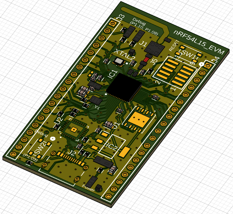
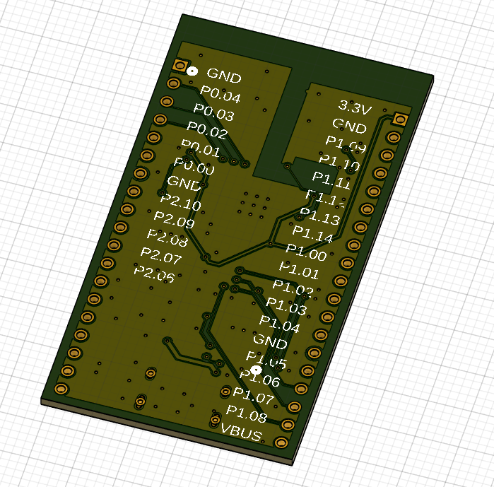
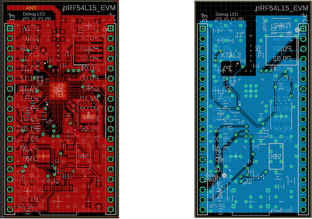
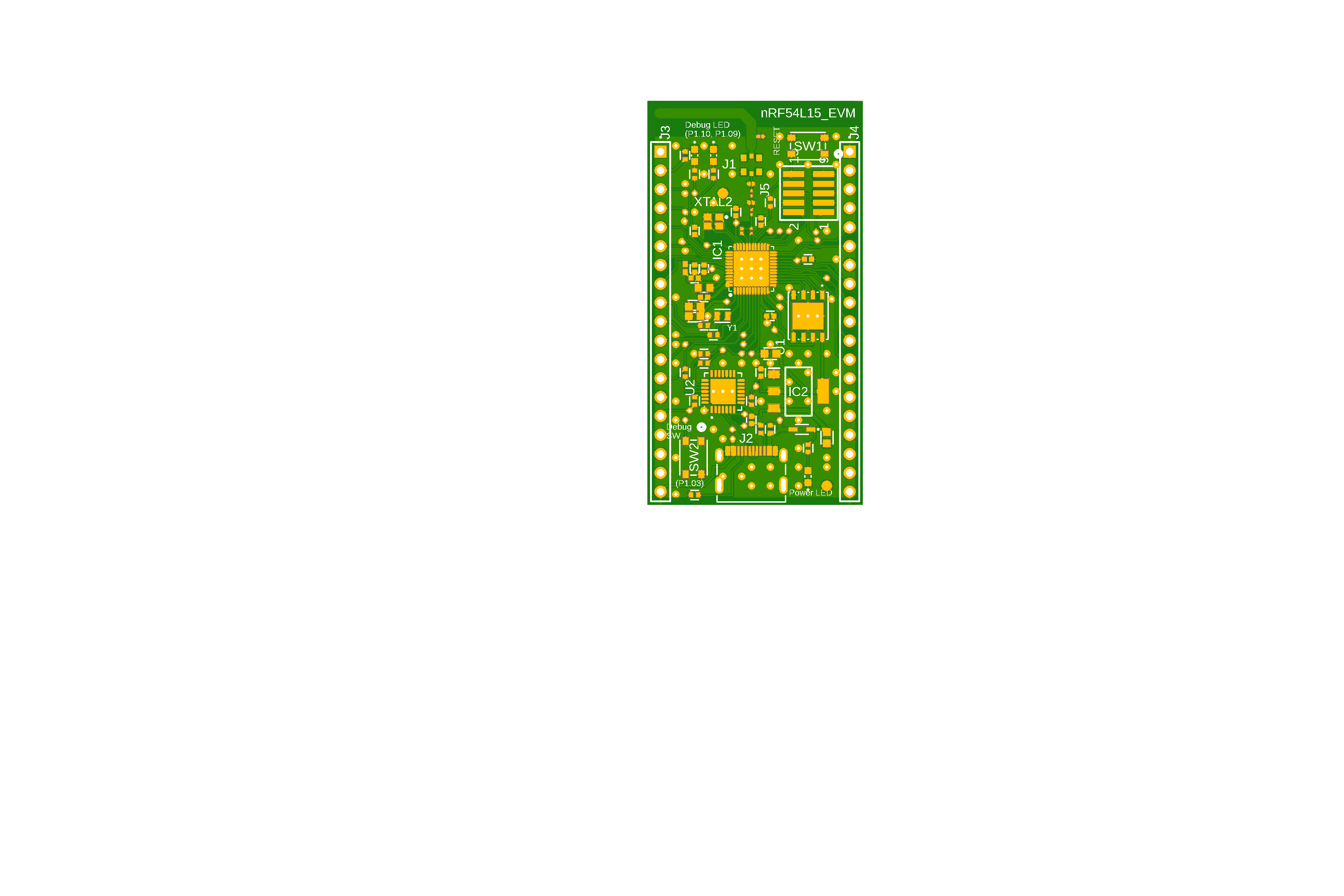
Maker's nRF54L15 Debug Board 2-layer PCB.
For details, Please refer to the AutodeskProjectfile(.f3z),Schematics(.pdf), Gerber(.zip) and BOM(.xlsx) files in the 'Schematics' section.
- The central component is the nRF54L15(IC1), a low-power wireless SOC.
- The board uses a Type-C connector (J2) for power input.
- There is a 5V-to-3.3V LDO regulator (IC2) to provide the necessary power supply for the nRF54L15 and other components. In this board, the external IO voltage level is also 3.3V.
- The design includes a CP2102N USB-to-UART converter (U2) to enable communication with a computer through a USB port. The UART pins of the CP2102N are connected to the nRF54L15.
- There is a Debug In Connector (J5), which is a Pin header for connecting an external debugger. This SWD (Serial Wire Debug) signal's interface allows the user to program and debug the nRF54L15.
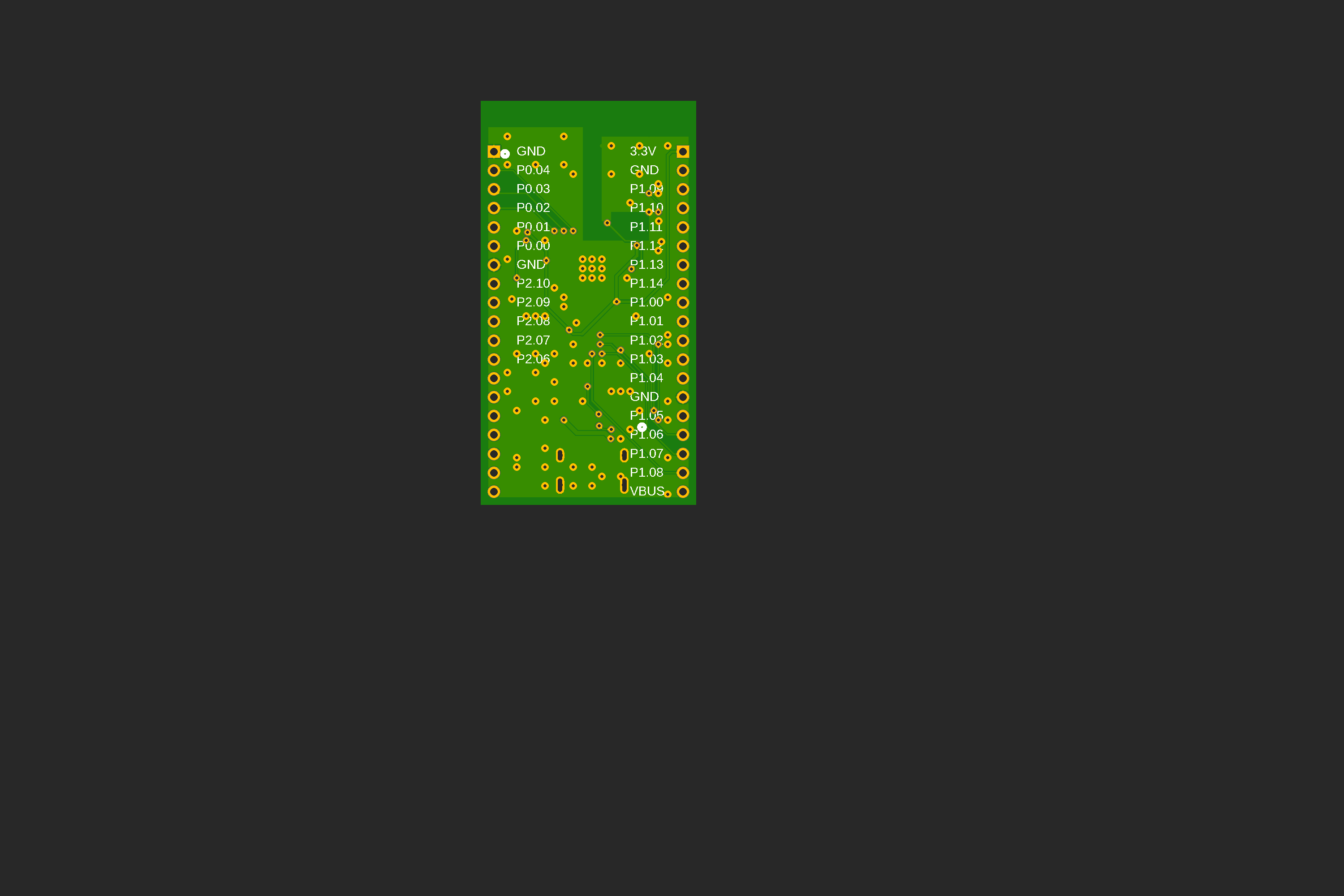
- 2.54mm GPIO connectors (J3, J4) provides access to a range of nRF54L15 GPIO pins for general-purpose use. This allows for easy connection to external sensors, actuators, or other hardware components.
- An external flash memory chip (U1) is included, probably to store user data. This chip communicates with the nRF54L15 via SPI interface.
- There is a RESET_SW(SW1) tactile switch for manually resetting the nRF54L15. The board also includes a DEBUG_SW (SW2) for a user definable purpose.
- Two User LEDs, one Red and one Green, are included for visual feedback. These are likely used to indicate power status or some operational state of the board.
All source code and board files(DeviceTree) for this project are available on GitHub.
https://github.com/iotengineer22/Board-Designer-Competition/tree/main
We chose Zephyr RTOS for this project. It offers scalability and a robust ecosystem for the nRF54L15. And, by using the Nordic Semiconductor nRF Connect SDK, software implementation is made easy.
- Zephyr RTOS: An open-source RTOS that is well-suited for this kind of embedded system.
- Nordic Semiconductor nRF Connect SDK: This SDK is a very useful tool for developing on a custom board for nRF54L15. We will also introduce practical debugging and usage methods. We use v2.9.0 version.
All source codes for projects are also available on GitHub.
https://github.com/iotengineer22/Board-Designer-Competition/tree/main/src/project
It's primarily based on modified sample code from Zephyr and nRF Connect SDK. Each test case has its own saved version. Original source links are provided in the description of each code.
The test program also references the two sample libraries mentioned above.
https://github.com/zephyrproject-rtos/zephyr/tree/main/samples
https://github.com/nrfconnect/sdk-nrf/tree/main/samples
4-2. Board file(DeviceTree)The original board(DeviceTree) files for this project are available on GitHub.
https://github.com/iotengineer22/Board-Designer-Competition/tree/main/src/board
- test_nrf54l15dk_nrf54l15_cpuapp.dts, dtsi (For ARM_M33)
- test_nrf54l15dk_nrf54l15_cpuflpr.dts, dtsi (For RISC-V)
Based on and modified from the Nordic nRF54L15-DK.
https://github.com/zephyrproject-rtos/zephyr/tree/main/boards/nordic/nrf54l15dk
They were created using the Nordic Semiconductor nRF Connect SDK within the nRF Connect for VS Code environment.
This setup allows anyone to replicate the development environment.
Basically, we use this board file in Build Configuration.
Here's an introduction to the software development environment used and the simple setup process. For details, please refer to the official link provided.
- nRF Connect for Desktop
https://www.nordicsemi.com/Products/Development-tools/nRF-Connect-for-Desktop
Although not used directly for this project, we installed this beginner-friendly desktop tool from Nordic. (It is noted to be convenient for getting started with official Nordic evaluation boards.)
In addition, the driver for programming the nRF54L15 was available for download at the same time.
- nRF Connect for VS Code Extension Pack(nRF Connect for VS Code)
https://www.nordicsemi.com/Products/Development-tools/nRF-Connect-for-VS-Code
For this project, we utilized the nRF Connect SDK via VS Code.
The nRF Connect SDK itself was also installed through the VS Code extension.
- nRF-Util
https://www.nordicsemi.com/Products/Development-tools/nRF-Util
Simply installing nRF Connect for VS Code was not sufficient to flash the nRF54L15, resulting in an error.
Flashing build to 1057787458 C:\Windows\system32\cmd.exe /d /s /c "west flash -d c:\boards\test\blinky_3\build --skip-rebuild --dev-id 1057787458"

-- west flash: using runner nrfutil -- runners.nrfutil: reset after flashing requested FATAL ERROR: required program nrfutil not found; install it or add its location to PATH
Therefore we reference Installation guide:
https://docs.nordicsemi.com/bundle/nrfutil/page/guides/installing.html
We downloaded nrfutil and placed it in the following folder within the nRF-SDK:
\ncs\toolchains\***<is your toolchain>\opt\bin\Scripts
To address this, we installed nRF Util via the command prompt. The nrfutil command becomes available after restarting.
C:\Users\***>curl https://files.nordicsemi.com/artifactory/swtools/external/nrfutil/executables/x86_64-pc-windows-msvc/nrfutil.exe -o nrfutil.exe

C:\Users\***>nrfutilThe nRF54L15 is equipped with interfaces. For details, please refer to the official nRF54L15 datasheet:
https://docs.nordicsemi.com/bundle/ps_nrf54L15/page/keyfeatures_html5.html
We introduce some of these interfaces that I debugged and tested, though not all of them.
5-1 Programming via SWDThe original nRF54L15 board is programmed using SWD (Serial Wire Debug). The SWD connector on this board is J5.
We use the nRF54L15 DK (Development Kit) and the Nordic Semiconductor nRF Connect SDK for programming.
You could also purchase and use an ARM debugger (like a J-link), but since the official board (nRF54L15-DK) was available, we chose to use it this time.
Connect the Debug OUT connector on the nRF54L15 DK to connector J5 on your board using a 10-pin cable with a 1.27mm pitch.
This bellow demo video explain how to program for nRF54L15 original board.
It is convenient that you can flash immediately after building using nRF Connect for VS Code.
After flashing, the change in the Custom board's LED lighting indicates successful programming.
GPIO debugging was performed. The board features onboard switches and LEDs, allowing for operation verification without external components.
Debug messages are also verified via USB serial (UART) through the Type-C connection. We use Silicon Labs CP2102N-A02-GQFN28R, as USB-UART IC on the board.
As the program is long, you can find it on GitHub. The following program was used for testing:
URL:https://github.com/iotengineer22/Board-Designer-Competition/tree/main/src/project/gpio
GPIO and UART device tree image are below. (For details, see the board file.)
led1: led_1 {
gpios = <&gpio1 10 GPIO_ACTIVE_HIGH>;
label = "Green LED 1";&pinctrl {
/omit-if-no-ref/ uart20_default: uart20_default {
group1 {
psels = <NRF_PSEL(UART_TX, 1, 4)>,
<NRF_PSEL(UART_RTS, 1, 6)>;
};
group2 {
psels = <NRF_PSEL(UART_RX, 1, 5)>,
<NRF_PSEL(UART_CTS, 1, 7)>;
bias-pull-up;
};
};The demo video is below:
The LED illuminates, confirming proper GPIO operation.
And, USB serial messages are successfully received via UART.
PWM debugging was carried out. An external servo motor (SG-90) is controlled by varying the PWM frequency.
As the program is long, you can find it on GitHub. The following program was used for testing:
URL:https://github.com/iotengineer22/Board-Designer-Competition/tree/main/src/project/pwm
5V power pin is available on the board, enabling operation directly from the board.
PWM device tree image is below. (For details, see the board file.)
/omit-if-no-ref/ pwm20_default: pwm20_default {
group1 {
psels = <NRF_PSEL(PWM_OUT0, 1, 14)>;
};
};The demo video is below:
We use nRF54L15 P1.14 pin as PWM.
The servo motor (SG-90) rotation angle is successfully controlled.
Oscilloscope measurements confirm the PWM frequency (600us-2400us) changes.
ADC (Analog-to-Digital Converter) debugging was performed. Analog measurements were taken by varying the voltage using external resistors and thermal sensor.
As the program is long, you can find it on GitHub. The following program was used for testing:
URL:https://github.com/iotengineer22/Board-Designer-Competition/tree/main/src/project/adc
ADC device tree image is below. (For details, see the overlay file.)
channel@0 {
reg = <0>;
zephyr,gain = "ADC_GAIN_1";
zephyr,reference = "ADC_REF_INTERNAL";
zephyr,acquisition-time = <ADC_ACQ_TIME_DEFAULT>;
zephyr,input-positive = <NRF_SAADC_AIN4>; /* P1.11 */
zephyr,resolution = <10>;
};
channel@1 {
reg = <1>;
zephyr,gain = "ADC_GAIN_1";
zephyr,reference = "ADC_REF_INTERNAL";
zephyr,acquisition-time = <ADC_ACQ_TIME_DEFAULT>;
zephyr,input-positive = <NRF_SAADC_AIN2>; /* P1.06 */
zephyr,resolution = <12>;
zephyr,oversampling = <8>;
};Note: This test requires the addition of an ADC device tree. We are using the configuration file for the nRF54L15-DK.
Make sure to configure it using "Extra Devicetree overlays" during board configuration.
The demo video is below:
Connected Register(47k + 10k_Variable) and Thermal sensor(LM35) with nRF54L15 on the breadboard.
And Checking Analog voltage with three ADCs.
Checking internal reference voltage. VREF≒0.9V... OK.
Changing variable register(10kΩ). Analog voltage ≒ (0V - 0.579V)...OK
*Vout_min = 3.3V * (0Ω / (47000Ω + 0Ω)) = 0V
*Vout_max = 3.3V * (10000Ω / (47000Ω + 10000Ω)) = 0.579V
Checking Thermal sensor (room temperature), and Heating the Thermal sensor with HOT Coffee. 241mV≒24℃ → 348mV≒35℃ ...OK.
We used LM35 Thermal sensor.
I2C (TWIM) debugging was performed.
Read/Write operations were verified using an external EEPROM. We used Atmel AT24C256.
As the program is long, you can find it on GitHub. The following program was used for testing:
URL:https://github.com/iotengineer22/Board-Designer-Competition/tree/main/src/project/i2c
I2C device tree image is below. (For details, see the board file.)
/omit-if-no-ref/ i2c21_default: i2c21_default {
group1 {
psels = <NRF_PSEL(TWIM_SDA, 1, 11)>,
<NRF_PSEL(TWIM_SCL, 1, 12)>;
};
};The demo video is below:
We connected SCL and SDA for EEPROM from nRF54L15.
SCL Clock setting is 100kHz.
Debug messages confirm successful I2C Read/Write operations.
We check I2C with Oscilloscope. (CH1_SCL, CH2_SDA)
The waveforms show that data 0xAA was written or read during the I2C communication.
Actual SCL clock Waveforms confirm 100kHz.
SPI debugging was performed. Read/Write operations were verified using the onboard FLASH (ROM).
We used Macronix MX25L6433FZNI-08G Flash(ROM).
As the program is long, you can find it on GitHub. The following program was used for testing:
https://github.com/iotengineer22/Board-Designer-Competition/tree/main/src/project/spi
SPI device tree image is below. (For details, see the board file.)
/omit-if-no-ref/ spi00_default: spi00_default {
group1 {
psels = <NRF_PSEL(SPIM_SCK, 2, 1)>,
<NRF_PSEL(SPIM_MOSI, 2, 2)>,
<NRF_PSEL(SPIM_MISO, 2, 4)>;
};
};The demo video is below:
nRF54L15 and Flash-ROM are on the board.
When the board is reset, the nRF54L15 communicates via SPI.
Debug messages confirm successful SPI Read/Write operations (0x55 0xAA 0x66 0x99).
I2S debugging was performed. An external I2S-DAC decoder and speaker were used to generate a beep sound.
Note: This is simple I2S demo. Since nRF54L15 doesn't have audio PLL, so we cannot have very accurate sampling frequency at 48KHz/24KHz/16KHz. And we cannot tune the sampling frequency to sync with transport layer (e.g., BLE), so there may be some restriction.
As the program is long, you can find it on GitHub. The following program was used for testing:
URL:https://github.com/iotengineer22/Board-Designer-Competition/tree/main/src/project/i2s
I2S device tree image is below. (For details, see the board file.)
/omit-if-no-ref/ i2s0_default_alt: i2s0_default_alt {
group1 {
psels = <NRF_PSEL(I2S_SCK_M, 1, 12)>,
<NRF_PSEL(I2S_LRCK_M, 1, 13)>,
<NRF_PSEL(I2S_SDOUT, 1, 11)>;
};
};The demo video is below:
Connected DAC + Speaker and nRF54L15 via I2S, and Preparing Beep Sound only.
We use MAX98357A, as I2S-DAC IC.
Reset and beep with i2S and nRF54L15.
This waveform means CH1_3.3V, CH2_BCLK, CH3_DIN, CH4_LRC.
The BCLK waveform was approximately 1.4 MHz. This is as expected based on the following calculation:
BLCK = 44100 Hz × 2 channels × 16 bits/channel = 1.4112 MHz
NFC debugging was performed. An external NFC Antenna were used, it was included in Nordic nRF54L15 DK.
Note: This is a simple NFC demo. Since the NFC antenna was modified using jumper wires for this demonstration and the NFC filter circuit diagram is not available, this circuit is not complete/standard.
As the program is long, you can find it on GitHub. The following program was used for testing:
URL:https://github.com/iotengineer22/Board-Designer-Competition/tree/main/src/project/nfc
The nRF54L15's dedicated NFCT peripheral and its corresponding NFCT_ANT1 and NFCT_ANT2 RF pins for NFC communication.
These are not standard GPIO pins like 1.02 or 1.03. The software configuration in prj.conf enables the NFCT hardware, and the device tree defines the peripheral, but the antenna pin connections are hardware-fixed.
CONFIG_NFC_T2T_NRFXLIB=y
CONFIG_NFC_NDEF=y
CONFIG_NFC_NDEF_MSG=y
CONFIG_NFC_NDEF_RECORD=y
CONFIG_NFC_NDEF_URI_REC=y
CONFIG_NFC_NDEF_LAUNCHAPP_MSG=yNFC Antenna is only connected directly. (not proper circuit diagram)
Details on the appropriate NFC circuit can be found in the following section of the datasheet.
https://docs.nordicsemi.com/bundle/ps_nrf54L15/page/nfct.html#ariaid-title11
The demo video is below:
We used "nRF NFC Toolbox" App for checking NFC communication.
It's a quick circuit this time: no filters, and the antenna is simply connected directly.
We need to have time to detect, but finally managed to detect as NFC Tag.
With a properly designed NFC, detection is quick.
When we use Nordic nRF54L15 DK, we can detect NFC tag info quickly.
If you are implementing an NFC connection, please refer to a proper circuit design, such as the one used on the nRF54L15-DK.
nRF54L15 is suitable for products using BLE, proprietary 2.4 GHz protocols, and more. We check some Bluetooth demo tests.
6-1. Bluetooth Low Energy (BLE)Bluetooth Low Energy(BLE) debugging was performed.
As the program is long, you can find it on GitHub. The following program was used for testing:
https://github.com/iotengineer22/Board-Designer-Competition/tree/main/src/project/lbs
Note: This project board file for this project does not support Non-Secure mode. Therefore, the NordicnRF54L15-DK board file is being used for this test.
The demo video is below:
Control GPIO with nRF54L15 and BLE from Tablet.
And Tablet App is "nRF Connect for Mobile".
Control GPIO with nRF54L15 and BLE from Tablet.
Finding and Connecting BLE device(My original nRF54L15 board) from App.
We can connect with BLE(Bluetooth Low Energy).
Checking Control GPIO(LED/SW) ON/OFF with BLE.
Bluetooth ISO(isochronous) Time Synchronization debugging was performed.
We check the synchronization between boards using Bluetooth ISO Time Synchronization.
As the program is long, you can find it on GitHub. The following program was used for testing:
https://github.com/iotengineer22/Board-Designer-Competition/tree/main/src/project/iso
The demo video is below:
Connected Bluetooth and nRF54L15 boards.
With Oscilloscope and LED, Check ISO Time Synchronization.
Setting transmitter/receiver, and Syncing start.
Input SW, Sync Output message and Sync Output LED... OK.
Checking Output Sync with Oscilloscope... OK.
We can check Sync Output waveform on the order of microseconds.
Bluetooth Mesh debugging was performed. (In this test, Initial Configuration check only.) Mesh is a type of network that lets many Bluetooth devices talk to each other.
As the program is long, you can find it on GitHub. The following program was used for testing:
https://github.com/iotengineer22/Board-Designer-Competition/tree/main/src/project/mesh
Note: This project board file for this project does not support Non-Secure mode. Therefore, the NordicnRF54L15-DK board file is being used for this test.
The demo video is below:
We use the "nRF Mesh" app on a tablet for mesh communication.
Bluetooth Mesh has been already initialized by nRF54L15.
Proceeding Identify and Provision for Mesh.
Setting OOB Type.(Adapting nRF54L15 for Output)
Authentication OOB.(Input OOB String: K)
Initial Configuration Complete.(But there are some steps for Mesh Chat.)
Bluetooth RSSI(dBm) debugging was performed. (In this test, We check and measure Bluetooth RSSI only.)
We compared the Nordic nRF54L15-DK with our custom board.
TAs the program is long, you can find it on GitHub. The following program was used for testing:
https://github.com/iotengineer22/Board-Designer-Competition/tree/main/src/project/lbs
This demo video is below:
In this test, scanning Bluetooth RSSI(dBm) with "nRF Connect" App.
The Nordic nRF54L15-DK has better Bluetooth performance than our custom PCB.
Our custom PCB has plenty of room for improvement in the antenna design.
The nRF54L15 SoC features a dedicated VPR CPU, based on the RISC-V architecture, called the Fast Lightweight Peripheral Processor (FLPR).
The nRF54L15 RISC-V are documented at https://docs.nordicsemi.com/bundle/ncs-latest/page/nrf/app_dev/device_guides/nrf54l/vpr_flpr.html.
This project board files for this chip include RISC-V(FLPR) configurations.
https://github.com/iotengineer22/Board-Designer-Competition/tree/main/src/board
- test_nrf54l15dk_nrf54l15_cpuflpr.dts, dtsi (For RISC-V)
When configuring the board file, selecting the FLPR option will automatically trigger a build process for it.
Additionally, we expanded the overlay snippet for nordic-flpr.We have also modified.yml files within the SDK, such as '\zephyr\snippets\nordic-flpr\snippet.yml`.
test_nrf54l15dk/nrf54l15/cpuapp:
append:
EXTRA_DTC_OVERLAY_FILE: boards/nrf54l15dk_nrf54l15_cpuapp.overlaynRF54L15 RISC-V GPIO + UART debugging was performed. We are checking the LED blinking and UART serial messages from a RISC-V core.
This RISC-V core is the FLPR, functioning as a generic core running the full Zephyr kernel.
As the program is long, you can find it on GitHub. The following program was used for testing:
https://github.com/iotengineer22/Board-Designer-Competition/tree/main/src/project/gpio
RISC -V UART device tree image is below. (For details, see the board file.)
/omit-if-no-ref/ uart30_default: uart30_default {
group1 {
psels = <NRF_PSEL(UART_TX, 0, 0)>,
<NRF_PSEL(UART_RTS, 0, 2)>;
};
group2 {
psels = <NRF_PSEL(UART_RX, 0, 1)>,
<NRF_PSEL(UART_CTS, 0, 3)>;
bias-pull-up;
};
};This demo video is below.
The program is already flashed onto the board. Resetting the board causes the RISC-V and Zephyr system to reboot.
Upon reboot, the LEDs repeatedly toggle ON/OFF, and serial messages are output via UART.
We are using an oscilloscope to examine the UART signal originating from the RISC-V.
Decoding the signal on the oscilloscope shows ASCII characters that correspond to the "LED state:".
The UART speed has been confirmed to be 115200 bps.
We debugged both the RISC-V and ARM_M33 cores on the nRF54L15 simultaneously.
We are checking the LED blinking and UART serial messages from a RISC-V core, and PWM Control from ARM_M33.
As the program is long, you can find it on GitHub. The following programs were used for testing:
https://github.com/iotengineer22/Board-Designer-Competition/tree/main/src/project/gpio
https://github.com/iotengineer22/Board-Designer-Competition/tree/main/src/project/pwm
When building for RISC-V, the sysbuild for the ARM_M33 core is also generated. We are implementing the PWM program in the main.c file for the ARM_M33 core.
For the ARM side, please note that the default Kconfig settings(prj.conf) are minimal, so you need to specify the PWM configurations.
CONFIG_STDOUT_CONSOLE=y
CONFIG_PRINTK=y
CONFIG_PWM=y
CONFIG_LOG=y
CONFIG_LOG_PRINTK=y
CONFIG_LOG_MODE_IMMEDIATE=y
CONFIG_PWM_LOG_LEVEL_DBG=y
# CONFIG_STDOUT_CONSOLE=y
# CONFIG_PRINTK=y
# CONFIG_LOG=y
# CONFIG_LOG_PRINTK=y
# CONFIG_LOG_MODE_IMMEDIATE=yThis demo video is below.
The nRF54L15 integrates both RISC-V and ARM M33 cores. In our debugging process, we controlled GPIO from the RISC-V core and PWM from the ARM_M33 core.
During debugging, serial messages were observed: ↑ indicates messages from the RISC-V core, and ↓ indicates messages from the ARM_M33 core.
We also performed reset and reboot operations for both the RISC-V and ARM_M33 cores.
Our tests confirmed successful control from each core:
- Control of GPIO + UART from the RISC-V core was successful (demonstrated by LED ON/OFF).
- Control of PWM + UART from the ARM_M33 core was successful (demonstrated by controlling a Servo Motor Pulse).
This section guides you through using Autodesk Fusion to modify and create your own Printed Circuit Boards (PCBs) based on a provided project file.
8-1. Free versionThe Autodesk Fusion design data for this project is readily available and accessible, allowing you to experiment and develop your unique board designs.
We'll cover downloading the free version of Autodesk Fusion, importing the project, and making modifications to the schematic, layout, and 3D model.
8-2. Video TutorialFor a visual walkthrough of the process, please refer to the following video in datil:
8-3. Downloading Autodesk FusionAutodesk offers a free version of Fusion 360 for personal, non-commercial use. This license provides ample functionality for hobbyists and makers to create impressive projects.
Notably, the provided PCB design data is fully compatible with the free version of Fusion 360, as it adheres to the limitations of the personal use license (2 layers + max area (L x W) of 80cm^2).
Download the free version here: https://www.autodesk.com/products/fusion-360/personal-form
8-4. Downloading the Project FileLocate the 'Schematics' section and download the file with the extension ".f3z". This archive contains all the necessary data for the project.
Launch Autodesk Fusion and upload the downloaded ".f3z" project file.
Fusion will automatically unpack the archive and open the project, providing you with access to the schematic, PCB layout (artwork), and the 3D model of the board.
Once the project is open, familiarize yourself with the three main components:
- Schematic: The electronic circuit diagram representing the connections between components.
- PCB Layout (Artwork): The physical design of the PCB, including component placement, traces, and vias.
- 3D Model: A visual representation of the assembled PCB, providing a realistic view of the final product.
Let's illustrate the modification process by changing an LED from Green to Blue.
- Download Component Library: Download the Digikey's LED library.
- Import Component Library: Import the downloaded library into Fusion 360.
- Replacing the LED in the Schematic: In the schematic view, locate the Green LED and replace it with the desired Blue LED from the imported library.
- Updating the PCB Layout: Switch to the PCB layout view. Replace the Green LED footprint with the corresponding Blue LED footprint. Furthermore, modify the board shape as desired.
After making changes to the schematic and PCB layout, update the 3D model to reflect those modifications. Fusion 360 will automatically generate a new 3D model based on the updated design. Verify that the LED color and board shape have been updated correctly in the 3D view.
Perform an ERC to check for issues in the schematic.Navigate to VALIDATE -> ERC to run the check. Approve any errors that are acceptable.
Perform a Design Rules Check (DRC) to check for issues in the artwork (layout).
Navigate to RULES -> Check Design Rules to run the check. Approve any errors that are acceptable.
If the schematic and artwork have no issues, output Gerber files.
Navigate to MANUFACTURING -> EXPORT Gerber, NC... to output all necessary data. You can find the Gerber, Drill, and Assembly data for the board manufacturer.
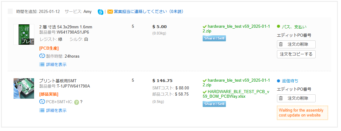
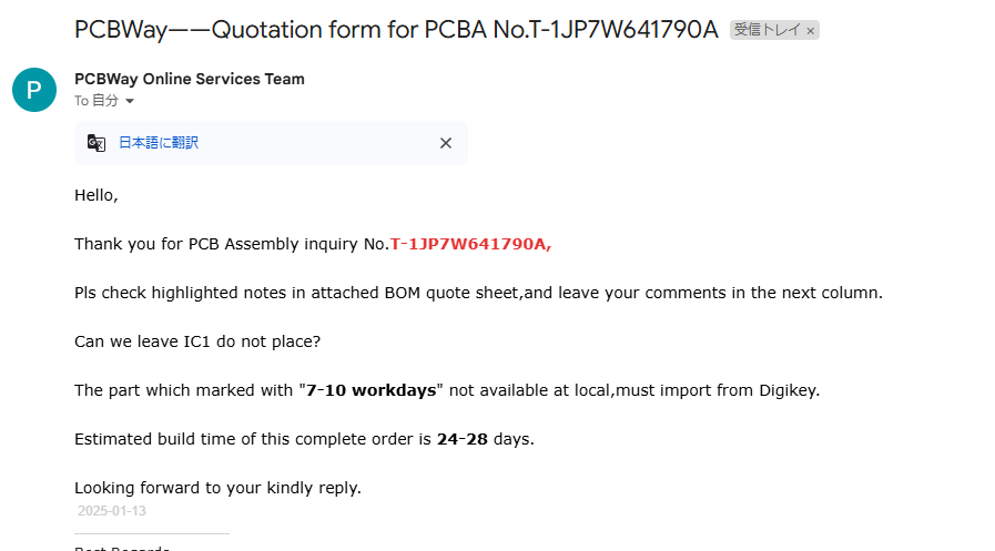
In this section, we introduce how to order the PCB using the outputted Gerber data and Bill of Materials (BOM) from PCBWay.
The Gerber data and BOM for the board ordered for this project are saved in the 'Schematics'. You can use these files to order the same board again.
The PCB Parameter settings, including the number of layers (2 layers) and board thickness (1.6mm), were mostly default.
Only the board size was entered manually: 54.30mm x 28.96mm. And, only SMT (Surface Mount Technology) components were used to reduce board assembly cost.
After placing the order, you just wait for the PCB to arrive.Based on personal experience, the total lead time was approximately 1 month (4 weeks).
Breakdown:
- Board Fabrication: approx. 1-2 days
- Board Assembly: approx. 3 weeks (includes approx. 2 weeks for component procurement due to the use of many ICs)
- Shipping: approx. 4 days
After delivery, you can power on the board by plugging in a Type-C cable.
Write and flash your desired program to test the board. (If you want to use the board with a breadboard, you can solder 2.54mm pitch pin headers.)
This section outlines the improvement points and future considerations identified during the debugging of the custom board.
10-1. Antenna DesignAs confirmed in Chapter 6-4, the RSSI (dBm) on the custom board was lower compared to the Nordic nRF54L15-DK. The antenna components used were essentially the same on both boards.
Likely Causes & Future Revision Points:
- Distance of Matching Circuit Components: The distance between the LC components of the matching circuit and the antenna is too large. Although space was intentionally left for potential adjustment, a more compact layout is recommended for improved performance.
- Impedance Matching & LC Tuning: Impedance matching on the board was not performed, and the LC values of the matching circuit were not fully tuned. (*Board impedance adjustment was omitted due to prioritizing PCB delivery time and cost. LC value tuning was not done due to debugging deadlines and the lack of an RF measurement environment.)
Recommendation: For similar future designs, it is highly recommended to refer to the Nordic datasheet and the layout patterns of the nRF54L15-DK, particularly the reference circuitry.https://docs.nordicsemi.com/bundle/ps_nrf54L15/page/chapters/ref_circuitry.html#ariaid-title4
10-2. SWD Connector PlacementThe Debug_in (SWD) connector was placed too close to the Reset SW.
While the current debug cable worked without interference, the positioning carries a risk of interference with the Reset SW depending on the specific cable connector used. (Reason: Board area was prioritized in this design.)
Recommendation: For better flexibility and ease of use in debugging environments, it is recommended to leave more space between the SWD connector and the Reset SW in future revisions.
10-3. On-board Debug Switch GPIO SelectionAlthough the on-board Debug SW using GPIO 1.03 functioned correctly, connecting it to GPIO 1.13 would have been more convenient.
Recommendation: Using GPIO 1.13 allows for easier reuse of the standard DK sample code without needing an external switch during development. (Reason: GPIO 1.13 is commonly used for BUTTON0 in Nordic's nRF54L15-DK sample programs.)
This project successfully achieved the following:
- Implemented Zephyr (RTOS) and Interface (SWD, GPIO, UART, PWM, ADC, I2C, SPI, I2S, NFC) on the nRF54L15.
- Bluetooth Debugging with nRF54L15. (BLE, ISO Time Synchronization, Mesh, RSSI)
- Integration of RISC-V and ARM M33 on nRF54L15.
- Introduction to the Design PCB of Autodesk Fusion.
This bellow video summarizes the main results.
This has been a greatfun challenge.
Thanks to to Nordic Semiconductor, Autodesk, PCBWay and hackster.io for hosting this exciting competition.
Thank you very much for all the support provided.


_t9PF3orMPd.png?auto=compress%2Cformat&w=40&h=40&fit=fillmax&bg=fff&dpr=2)


_SPmZ63wPgQ.png?auto=compress%2Cformat&w=40&h=40&fit=fillmax&bg=fff&dpr=2)
Comments