


Hardware components | ||||||
 |
| × | 1 | |||
| × | 1 | ||||
 |
| × | 1 | |||
| × | 1 | ||||
 |
| × | 1 | |||
Software apps and online services | ||||||
 |
| |||||
One week ago, the A-list rappers at SoundCloud came to us with a cryptic message:
48 65 6c 70 20 75 73 20 6d 61 6b 65 20 73 75 70 61 20 68 6f 74 20 66 69 72 65 20 70 6c 73 73 73
After being way too extra and building a modified version of the Enigma machine to crack the code, we realized that the message was simply a string of Hex mapped to ASCII characters. "Eureka!!!" we shouted as we scrambled to decipher the message. Ten minutes later, we had our challenge:
"Help us make supa hot fire plsss"
Our lives flashed before our eyes as we realized the task before us. The union of SoundCloud rappers had just asked us to help revolutionize the world of music and join the fight against Taylor Swift's domination of the Billboard Hot 100.
"But what can we offer that Taylor Swift doesn't already have??" Austin and I asked ourselves.
"Ahhhhhh" said Shaan as he looked up from his book. "She may have some sick beats, but she DOESN'T have our Piezo buzzer"
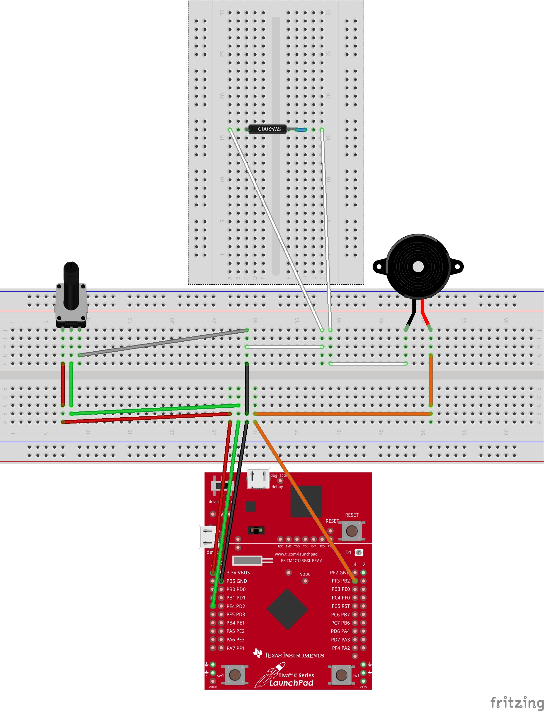
The BuildArmed with the latest and greatest technology (aka our Seeed Sidekit Basic Kit and a Texas Instruments Launchpad lol), fueled by Shaan's E X T R A T H I C C PB&J sandwiches, and with the words of the late Professor Simar echoing in our heads ("schedule is critical...schedule is critical...schedule is critical..."), we hammered away at our latest innovation.
With Shaan keying in the software, Austin playing with circuits, and me typing up this story, we made our first breakthrough (WOW!!!).
For our first major design decision, we decided that if we were to compete with Taylor Swift, we would have to forego using more simplistic circuits and instead go all out with our design; this meant that rather than using limited-voltage-range circuits, only circuits with a voltage range of 0-3.3 volts would do.
Along the way (kinda randomly) a higher power gifted us a Speed-UP-Time-Stone, and we were able to accelerate the development of our product....shrinking our production timeline from 3 years to just 7 days (WOW!!!!).
The final fruits of our label can be seen below:
On April 23rd, 2020, team "Help! We're trapped in our basement and can't get out!" delivered on their promise and fundamentally altered the world of sound engineering.
While officially recognized as the "HarRay POTentiomeTER and the Half-Heard Piezo," the product has since become known as "H-Pot" after SnoopDogg and other popular artists were spotted getting high off of its sick beats.
Indeed, it seems the world has also fallen in love with "H-Pot." It's an insider secret, and one that is jealously protected, but the melody and beat from Roddy Ricch's "The Box" were both almost exclusively sampled from "H-Pot's" frequencies. The effect? At the time of writing, the song has been at the top of the Billboard Hot 100 for 11 straight weeks.
Not bad for a breadboard, processor, and little piezo buzzer.


Comments