

Hardware components | ||||||
 |
| × | 1 | |||
 |
| × | 1 | |||
Software apps and online services | ||||||
_4YUDWziWQ8.png?auto=compress%2Cformat&w=48&h=48&fit=fill&bg=ffffff) |
| |||||
Hand tools and fabrication machines | ||||||
 |
| |||||
You might've heard of Shitty Add-Ons by now; if not, just search #BadgeLife on Twitter or Instagram, and you'll find a ton of cool designs that are meant to attach to a PCB conference badge (if it has the right ports). It's an I2C interface, which can be used for some complex applications but will also power a simple LED + resistor circuit with 3.3 volts.
The SAO standard footprint is published for KiCad, so we'll be using that to create our add-on. And I happen to have a Bantam desktop PCB mill on loan, which is great because Supercon is in five days and I can play with a lot of designs before then!
I work on a Mac, so this is my process for that; if you're using Windows, check out Chris Gammell's Getting to Blinky tutorial to clear up any confusion. And if you're new to KiCad, Nate Seidle's KiCad tutorials on SparkFun may also help a bit! I'm still new to PCB design, so be sure to check out the links I reference if anything seems unclear. :)
0. What are we doing, exactly?We're going to design a simple add-on that powers an LED through a resistor. Check out this wonderful example by Andrew Sowa:
Notice that only the VCC and GND pins are connected; that's because this is a very simple design with no real "smarts". We'll be doing the same.
If you have some experience and want to skip ahead, you can grab the files for this one off GitHub and mod them.
You can also order some SAO-compatible proto boards from OSH Park to try out different designs before taking the plunge.
And if you want to get REAL FANCY, check out this PCB art tutorial we recorded with Andy!
1. Grab some files and get set upFirst things first: head to Brian's original project and grab the connector library file (.lib).
Then, you'll need to drop it into KiCad's libraries folder: Macintosh HD > Library > Application Support > kicad > library
Create a new project in KiCad, open Eeschema, and go to Preferences > Component Libraries. Hit "Add" and browse to find the new library, then finish the process.
Still in Eeschema, hit "a" to add the connector to your schematic:
From here, everything is the same as your standard PCB layout, but since I still need practice, I'll give you the quick version as I work through it.
2. Add componentsNext things next, I've just added my LED and resistor. To do that, I hit "a" again, then searched for the generic LED and resistor components and place them on the schematic. I hit "R" to rotate them into sensible placements. After that, I used the Wire tool to connect them up.
I added values and labels by double-clicking on each component with the regular cursor tool.
Now, I had to juggle some stuff. I figured I'll keep the footprint for the SAO connector in its own little project folder, which I'll probably leave in the same place in my Downloads folder (don't judge me). So, I manually created an "sao.pretty" folder, within this project, and placed inside it the "Badgelife-Shitty-2x2.kicad_mod" file that I got from Brian's project:
And then I opened the PCB layout tool and used Preferences > Footprint Libraries Manager to add this to my globally available footprint libraries. (See this GtB video for details.)
Next, I used Eeschema's Cvpcb tool to link the SAO component footprint – and the LED + resistor component footprints – to my project. I had to manually measure my resistor to find a good match, which was a little nerve-wracking, but I settled on a through-hole one that had a reasonable pitch and called it a day. It has the wonderful name of "Resistors_THT:R_Axial_DIN0207_L6.3mm_D2.5mm_P7.62mm_Horizontal". I mean, I guess it's descriptive?
Lo and behold, the SAO footprint library was actually there when I went to look for it!!! I am so, so grateful that things didn't get hung up at this point, since I've hit 10pm and my brainpower is waning. :) Here's my final set of associations:
OK! Now we've finally gotten to the creative part. :) Hit the big green NET button to generate a netlist and create your layout file! (If you've already messed around with it, you may be asked whether or not to overwrite. Go on ahead.)
Now, open up Kicad's Pcbnew tool. Oh nooo, where are all your components? Well, you have to hit the big green NET button here, as well. Click "Read Current Netlist", and it'll pull in all of your components and connections from the schematic. Hooray! Close the window.
Of course, they're all grossed up on top of each other:
Here, I started leaning heavily on video 7 in Chris's GtB series: Creating the Layout.
Click the "Mode footprint" tool in the top toolbar, then right-click in your layout and choose Global Spread and Place > Spread out All Footprints:
Now we're getting somewheres! (The other components have been placed outside the footprint of the Badgelife connector, which includes a big yellow rectangle. More on that later...)
To move a component, mouse over it and hit M.
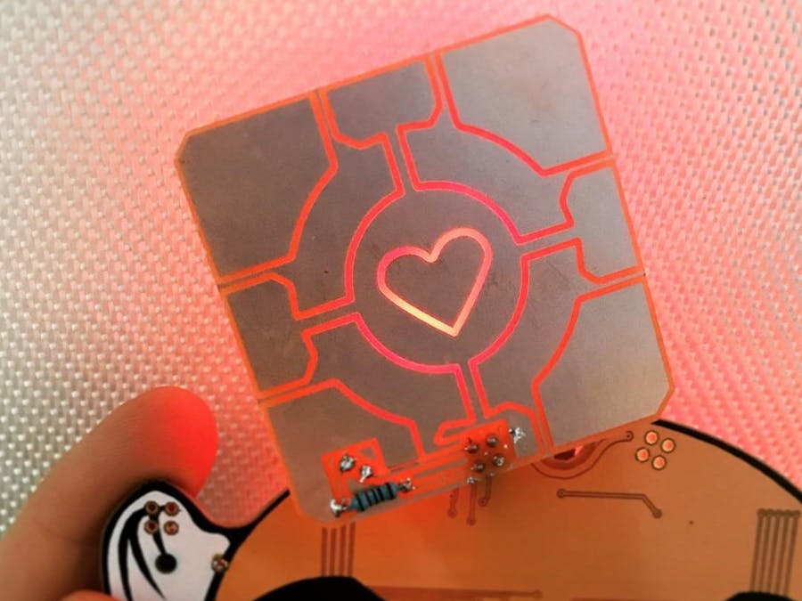
So, the connector footprint includes a big rectangle. Hmm... Well, it's a square. So why not make our first board a Companion Cube from Portal? It will be a little complex, but I can put everything on the bottom, so that it's illuminated from behind. ^_^
I found this CC BY 3.0-licensed Companion Cube SVG by Travis Lucia on Inventables and downloaded it. Then, I looked up the requirements for the Bantam desktop mill. From KiCad, the mill wants a Gerber file with at least the top copper layer and edge cuts. That's fine – I want to solder everything on the top, but have the components sit on the bottom. With through-hole components, that's no problem!
Grab the resistor with the move tool (M), then hit F to flip it to the bottom of the board. Do the same with the LED.
At this point, I realized that I needed to swap the resistor and LED in the circuit since they', so I went back to edit the schematic file, re-netted everything, and had a pretty painless time reconfiguring it. I also learned that you can rotate a component 45 degrees (or other arbitrary value) by editing the parameters – just hit E.
Now, it's time to join our friend Mr. Sowa on YouTube. Recall that I have an SVG of my chosen design, which is great because I can easily open it in Inkscape. I need the design to be black where the copper should be, and that's already how it is. Great!
I opened the SAO footprint in the footprint editor (right-click > Footprint... > Edit with Footprint Editor) and changed the grid to 5mm because it's now 11pm and I can't be bothered to find the right place to see its dimensions. ;) It's 50mm square, which is almost exactly 2 inches – 1.97, to be exact. So, as our maestro says, we need an exported PNG at about 400dpi. Multiplying 1.97*400, I get 788, so that's how many pixels square the exported PNG should be. (Andrew has emphasized often that it's easiest to resize your image before it gets into KiCad, so I'm making sure to do that.)
Turns out, it's not perfectly square, so I round down to get a little border around the metal design. That'll camouflage any imprecision. 750px by 742, hooray. This file goes into my project folder.
Since I only have a single copper layer, I can skip ahead to about 24:00 in the workshop. I open the new PNG file in KiCad's Bitmap2Component tool; for some reason, it bumps it down to 96 DPI. When I readjust it, it comes in at 47.6 x 47.1mm... perfect!
I export that as "cube", and now my KiCad project shows a new file, "cube.kicad_mod". Now, I can skip ahead to 28:30 in the tutorial, where we mess around with the files manually to make them into a single footprint (usually, you'll have copper, solder mask, and silkscreen layers). Again, I just have one layer – but it's the copper layer, so I need to edit the file to change it from "Front silk screen". I open cube.kicad_mod in my text editor of choice, and do a find-and-replace: "F.SilkS" becomes "F.Cu".
I go into KiCad, open the Footprint Editor, and choose File > Load Footprint > Import Footprint From File. Beautiful! There's some random text in there, but that won't even show up on the copper layer; it goes away if I uncheck "Hidden Text" under the "Render" tab, so I'm assuming it isn't even something that will be visible in the end. I throw this into its own.pretty folder within my project, and call it good enough.
(For those curious, the proper way to edit footprints is to make sure you have the right Active Library selected and follow one of the pro tutorials I've linked above. This works so far, and it's way easier for me, so [exaggerated shrug]...)
A few more steps:
- Load the footprint into KiCad's Pcbnew tool (the layout designer); this requires some searching for the file, but it's easy if you click "List All" in the dialog.
- Move everything around so it's pretty
- Edit SAO footprint to move connector closer to the edge: I did this purely for aesthetics. The footprint editor is in the top toolbar in Pcbnew, but also available from the KiCad main window. To get this new footprint to load, I had to save it out to a new file, change it in the schematic, and re-net in Eeschema and Pcbnew... but it worked!
- Add tracks and vias: Double-click to end a track; the rat's nest line may not immediately vanish, like it does in Chris's video, but will when the screen refreshes for some reason. :)
I went to View > 3D Viewer to check that everything was hooked up correctly. Looks like the SAO Connector footprint has a right-angle header stuck in it, which I neglected to move when I edited it, so that's just kinda jankily stuck in the middle – but no worries! The short li'l LED legs will actually be left long, so that I can solder it near the end of the legs, then bend it in to shine towards the middle.
5. Edit art around circuit; add edge cutsNoooo! The 3D view also showed me that KiCad doesn't override the custom copper footprint to add an offset zone around my circuit traces. That means all my pins would be connected, and the 3.3V would flow directly into the GND pin, shorting something out or at least disabling the add-on.
...So, I go back and edit the.png to put in some massive cutouts, re-import, re-replace with F.Cu, re-save in a new library, and re-import the new footprint. It juuuuuuuuust fits:
I also learned here (HERE!) that the SAO connector's yellow rectangle isn't actually on the Edge Cuts layer... it's on F.Fab, which is just for documentation and doesn't affect the PCB at all! It just happens to exactly match the color of the Edge Cuts layer. 🤦🏻♀️
So, I clicked on Edge Cuts and used the "Add graphic line or polygon" tool (the dashed line on the right) to draw a tighter outline around the cube design. Nice!
OK! Export time! At this point, we have a one-sided PCB that can be made on a Bantam desktop mill. There are a couple of close spots – which require a smaller tool, or could be hit manually with a Dremel – and the traces are a little thin. If I get some free time, I might play with the KiCad settings to make the drill holes and traces/offsets bigger. But in general, it looks pretty good!
I'm a little sad that the big black areas in the image won't be milled out, disabling the awesome backlit effect... but that's an issue specific to this tool, so stay tuned for the Bantam PCB milling tutorial and we'll see if I manage to fix it!
You can also test how it uploads to OSH Park and get a preview of how the finished board would look! I put this one up, and it automatically applied solder mask over the whole thing – so I'd have to address that in the footprint (as in the art PCB workshop) if I wanted to get it manufactured. I should also add a note in the footprint attributing the creator of the SVG.
Of course, if you want to get more intense with your design, you can check out the other tutorials I've linked here.
Hack on!


_Ujn5WoVOOu.png?auto=compress%2Cformat&w=40&h=40&fit=fillmax&bg=fff&dpr=2)


Comments