The Arduino MKR boards only have a limited number of GPIOs. The MKR Vidor 4000 is different because it has a FPGA to support its main microcontroller. Many of the FPGA pins are available on the Mini PCIe connector. So I took a closer look at this connector and wanted to see which functions are available at these pins.
This connector has 52 positions and the pinout can be grabbed from the official schematics of the board. The following table shows the pins with its functions on Vidor and on regular mPCIe:
pin   on Vidor           on mCPIe  ||   on mPCIe   on Vidor     pin
 1    WM_PIO2/PEX_PIN1   WAKE#     ||   +3V3AUX    +3V3          2
 3    WM_PIO3/PEX_PIN3   COEX1     ||   GND        GND           4
 5    WM_PIO4/PEX_PIN5   COEX2     ||   +1.5V      PEX_PIN6      6
 7    WM_PIO34/PEX_PIN7  CLKREQ#   ||   UIM_PWR    PEX_PIN8      8
 9    GND                GND       ||   UIM_DATA   PEX_PIN10    10
11    PEX_PIN11          REFCLK-   ||   UIM_CLK    PEX_PIN12    12
13    PEX_PIN13          REFCLK+   ||   UIM_RESET  PEX_PIN14    14
15    GND                GND       ||   UIM_VPP    PEX_PIN16    16
17    WM_PIO24           RESERVED  ||   GND        GND          18
19    WM_PIO25           RESERVED  ||   W_DISABLE# PEX_PIN20    20
21    GND                GND       ||   PERST#     PEX_RST      22
23    PEX_PIN23          PERn0     ||   +3.3VAUX   +3V3         24
25    PEX_PIN25          PERp0     ||   GND        GND          26
27    GND                GND       ||   +1.5V      PEX_PIN28    28
29    GND                GND       ||   SMB_CLK    PEX_PIN30    30
31    PEX_PIN31          PETn0     ||   SMB_DATA   PEX_PIN32    32
33    PEX_PIN33          PETp0     ||   GND        GND          34
35    GND                GND       ||   USB_D-     USB_DM       36
37    GND                GND       ||   USB_D+     USB_DP       38
39    +3V3               +3.3VAUX  ||   GND        GND          40
41    +3V3               +3.3VAUX  ||   LED_WWAN#  PEX_PIN42    42
43    GND                GND       ||   LED_WLAN#  PEX_PIN44    44
45    PEX_PIN45          RESERVED  ||   LED_WPAN#  PEX_PIN46    46
47    PEX_PIN47          RESERVED  ||   +1.5V      PEX_PIN48    48
49    PEX_PIN49          RESERVED  ||   GND        GND          50
51    PEX_PIN51          RESERVED  ||   +3.3VAUX   +3V3         52
This shows that the Vidor is somehow compatible to any standard Mini PCIe header used in computers. At least the GND and 3.3V pins are at the same location as well as the USB pins. On the Vidor the USB pins on the Mini PCIe connector are directly connected to the Micro USB connector on the other end of the board. So when plugged into a Mini PCIe socket on a computer it might be possible to programm the Vidor without using an additional USB cable.
After reset and when nothing is programmed all these pins are inputs. So nothing bad should happen if you plug it into your computer. But care must be taken when you programm the pins. Putting a high level (3.3V) on some of the 1.5V pins might carry some risk of damage.
Using the pins as GPIOs is quite simple. Actually it is already shown in the VidorTestSketch ( https://github.com/vidor-libraries/VidorPeripherals/blob/master/examples/VidorTestSketch/VidorTestSketch.ino ):
 // Ok, so we know now that the FPGA contains the extended GPIO IP
// Please refer to the online documentation for the actual pin assignment
// Let's configure pin A0 to be an output, controlled by the FPGA
 FPGA.pinMode(33, OUTPUT);
 FPGA.digitalWrite(33, HIGH);
The difficult part is to figure out why they use 33 as pin number. It is somehow common knowledge that MKR pins (AREF, A0..A6, D0..D14) have the numbers 32 to 54 assigned. So A0 is 33, A1 is 34 and so on. D14 is 54.
But what about the pins on the Mini PCIe connector? When you dig deep into the Arduino Vidor Forum you find a spreadsheet with the mapping:
https://docs.google.com/spreadsheets/d/1oAL1Iz39eCHi0IVyMiTRyekmzJg5TgeyO5t0fN6Vl4U/edit#gid=0
The tab "miniPCIe pinout" shows the mapping.
pin   name         number in FPGA
22    PEX_RST      0
6     PEX_PIN6     1
8     PEX_PIN8     2
10    PEX_PIN10    3
12    PEX_PIN12    4
14    PEX_PIN14    5
16    PEX_PIN16    6
20    PEX_PIN20    7
28    PEX_PIN28    8
30    PEX_PIN30    9
32    PEX_PIN32    10
42    PEX_PIN42    11
44    PEX_PIN44    12
45    PEX_PIN45    13
46    PEX_PIN46    14
47    PEX_PIN47    15
48    PEX_PIN48    16
49    PEX_PIN49    17
51    PEX_PIN51    18
11    PEX_PIN11    19    this pin is only an input
13    PEX_PIN13    20    this pin is only an input
23    PEX_PIN23    21    this pin is only an input
25    PEX_PIN25    22    this pin is only an input
31    PEX_PIN31    23    this pin is only an input
33    PEX_PIN33    24    this pin is only an input
And for my test this proved to be right.
VidorBreakout boardTo access the pins one could directly solder cables to the pads which is a bit tricky or use an adapter. I couldn't find a good adapter so I made my own. You can find the data here:
https://github.com/generationmake/VidorBreakout
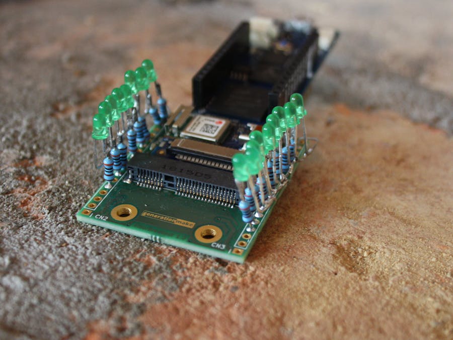
The breakoutboard connects all GND and 3.3V pins together and brings only the GPIOs seperately to the pinheader. Additionally the Vidor can be directly srewed onto the adapter with a M2.5 screw and both form a solid unit.
The design was made using 3D models and FreeCAD so that there is no collision.
The adapter follows the 2.54 mm grid of the Vidor. So both could plugged into a breadboard. Althought you would need a special breadboard because the adapter is wider than a regular breadboard.
To demonstrate the function of the GPIOs and the adapter I made a LED sequence using 17 green 3mm LEDs with a 3.3 kOhm resistor connected to ground.
Unfortunately I couldn't find any more functions which are supported on the Mini PCIe connector pins. Hopefully this changes in the future.
The breakoutboard and parts are available at Aisler: https://aisler.net/generationmake/playground/vidorbreakout


Comments