

The purpose of this laboratory/project was to implement hardware timer interrupts and a foreground/background task scheduling system on the STM32F407ZGT6-based RT-Spark development board. Two hardware timers, TIM2 and TIM3, were configured to toggle two onboard LEDs at different rates, and an external interrupt was set up on the KEY_UP button (PC5) to instantly toggle both LEDs when pressed. The system follows a cyclic executive architecture where ISRs handle urgent background work and set flags, while the main loop processes the actual tasks in the foreground.
NOTE: The handout/file originally instructed the use of PA0 for the button interrupt. After testing and checking, PA0 has no physical button connected to it on the RT-Spark board.
DESIGN AND TESTINGPart 1 — HARDWARE DESCRIPTIONThe hardware used was the RT-Spark development board built around the STM32F407ZGT6 microcontroller. No external components were needed since the board already has two onboard LEDs and directional buttons. The pin assignments are:
PART 1.1 — SOFTWARE SETUP
- Open STM32CubeMX
- Go to File → New → STM32 Project
- In the chip selector, search for STM32F407ZGT6 and select it
- Click Next
- Go to Project Manager, Set your preferred Project Name
- Set Toolchain/IDE to STM32CubeIDE
- Save the Project under File at the top left corner or just press Ctrl + S
PART 1.2 — CONFIGURING GPIO PINS FOR LEDs
- In the Pinout & Configuration tab, find pin PF11
- Click it and set it to GPIO_Output
- Go to System Core → GPIO, click PF11 and set User Label to LED_RED
- Find pin PF12, set it to GPIO_Output
- Set User Label to LED_BLUE
- Save the project and generate code
PART 1.3 — CONFIGURING THE SYSTEM CLOCK
Before setting up the timers, the system clock needs to be running at 84 MHz. By default, CubeMX generates code that runs on the raw HSI at 16 MHz — this makes the timer calculations completely wrong. This was the first issue encountered during this lab/project, 3 the LED stayed ON constantly because the ARR was also set to the maximum value of 4, 294, 967, 295 instead of 9999.
- Go to the Clock Configuration tab
- Find the HCLK box and type 84, then press Enter
- CubeMX will automatically configure the PLL to reach 84 MHz
- Save and regenerate code
PART 1.4 — CONFIGURING TIM2 AND TIM3
TIM2 fires every 1 second (1 Hz) and TIM3 every 0.5 seconds (2 Hz). The timer period formula from Lecture 2 is: f_timer = f_APB / (PSC + 1) / (ARR + 1)
For TIM2: 84, 000, 000 / (8399+1) / (9999+1) = 1 Hz
For TIM3: 84, 000, 000 / (8399+1) / (4999+1) = 2 Hz
Steps in CubeMX:
- Go to Timers → TIM2, set Clock Source to Internal Clock
- Set Prescaler to 8399 and Counter Period to 9999
- Under NVIC Settings, enable TIM2 global interrupt,
- set Priority to 0
- Go to Timers → TIM3, set Clock Source to Internal Clock
- Set Prescaler to 8399 and Counter Period to 4999
- Under NVIC Settings, enable TIM3 global interrupt,
- set Priority to 1
- Go to System Core → NVIC and confirm priorities
- Save and regenerate code
PART 1.5 — CONFIGURING THE DEBUG PIN
PE0 is configured as DEBUG_PIN for timing measurements.
This pin is toggled at the start and end of the TIM2 ISR
and Task A, allowing TISR and TTask to be measured using
the DWT cycle counter.
- Find pin PE0 → set to GPIO_Output
- Go to System Core → GPIO, click PE0 and set
- User Label to DEBUG_PIN
- Save and regenerate code
PART 1.6 — CONFIGURING THE BUTTON
The lab originally instructed PA0, but PA0 has no physical button on the RT-Spark board. After checking the RT-Thread documentation, KEY_UP is on PC5. PC5 was used instead. The lab also instructed Rising edge + Pull-down. However, the KEY_UP button is Active LOW on this board, it connects to GND when pressed. Falling edge + Pull-up is the correct configuration..
- Find pin PC5 → set to GPIO_EXTI5
- Go to System Core → GPIO, click PC5 and set:
- GPIO mode: External Interrupt Mode with Falling edge
- GPIO Pull-up/Pull-down: Pull-up
- Go to System Core → NVIC, enable EXTI line[9:5] interrupts, set Priority to 2
PART 2.1 — FOREGROUND/BACKGROUND ARCHITECTURE
The system uses a cyclic executive with interrupts. There are two priority levels: Background (ISRs) — run when triggered, handle urgent work, set flags to signal the foreground.
Foreground (Main loop) — runs continuously, checks flags, and executes the actual tasks. This is more efficient than polling with HAL_Delay() because the CPU is free to do other work between timer events.PART 2.2 — GLOBAL FLAG VARIABLES
The three flag variables are declared volatile so the compiler does not optimize out the reads in the main loop:
volatile uint8_t task_adc_ready = 0;
volatile uint8_t task_display_ready = 0;
volatile uint32_t tick_count = 0;
PART 2.3 — TIMER CALLBACK (BACKGROUND TASKS)
The HAL timer callback handles both TIM2 and TIM3 in one function. The htim->Instance field identifies which timer fired:
PART 2.4 — MAIN LOOP (FOREGROUND TASKS)
PART 2.5 — BUTTON ISR (EVENT-TRIGGERED)
PART 3.1 — LED BLINK OUTPUT
After flashing the code, the following was observed:
- Red LED blinks every 1 second via TIM2 interrupt
- Green LED blinks every 0.5 seconds via TIM3 interrupt
- Pressing KEY_UP (PC5) instantly toggles both LEDs
- Foreground/background scheduling working correctly
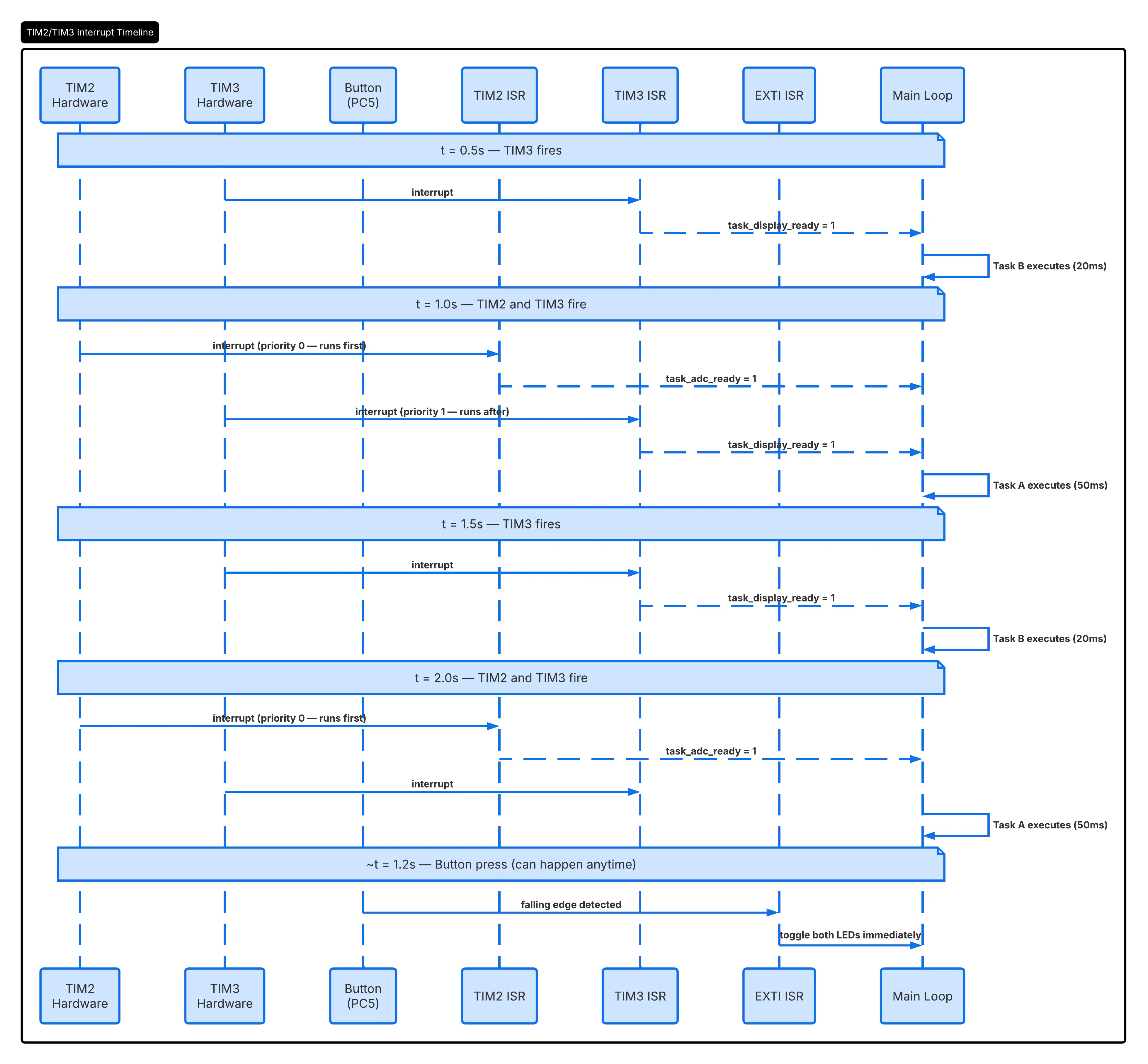
PART 3.2 — SEQUENCE DIAGRAM
The sequence diagram below shows 3 seconds of system operation including TIM2 and TIM3 firing at their respective rates, flags being passed to the main loop, and a button press event at approximately t=1.2 seconds. This was created using Lucidchart.
PART 3.3 — TIMING MEASUREMENTS
Real timing values were obtained using the DWT (Data Watchpoint and Trace) cycle counter on the ARM Cortex-M4. This is a 32-bit register that counts CPU clock cycles at 84 MHz precision (1 cycle ≈ 11.9 ns). The DWT counter was enabled in code:
CoreDebug->DEMCR |= CoreDebug_DEMCR_TRCENA_Msk;
DWT->CYCCNT = 0;
DWT->CTRL |= DWT_CTRL_CYCCNTENA_Msk;
Breakpoints were placed at the entry/exit of the TIM2 ISR for TISR, and at task_adc_ready = 1 and if (task_adc_ready for TLatency. The DWT->CYCCNT register was read at each breakpoint using the Expressions window in STM32CubeIDE.
TISR Measurement:
DWT at ISR start (line 69): 246
DWT at ISR end (line 76): 346
Clock cycles: 346 - 246 = 100 cycles
Time: 100 / 84, 000, 000 = 1.19 µs
TLatency Measurement:
DWT at task_adc_ready = 1: 44, 094, 304
DWT at if(task_adc_ready): 50, 141, 984
Clock cycles: 50, 141, 984 - 44, 094, 304 = 6, 047, 680 cycles
Time: 6, 047, 680 / 84, 000, 000 = 72 ms
TIMING TABLE:
The 72 ms latency is higher than the theoretical 20 ms estimate. This is because it includes not just Task B's HAL_Delay(20), but also the time for the ISR to finish, return to the main loop, and loop back around to the task_adc_ready check. This matches closely with what was expected given the system design.
PART 4 - ANALYSISWHAT I LEARNED:
This lab showed the practical difference between polling and interrupt-based scheduling. Using hardware timers removes the need for HAL_Delay() in the main loop, which frees the CPU to do other work between events. The foreground/background architecture is a clean and simple way to handle multiple tasks at different rates without a full RTOS. The DWT cycle counter was a useful tool — the measured TISR of 1.19 µs confirms that keeping ISRs short is important since the entire TIM2 ISR executes in just 100 clock cycles.
ISSUES FACED:
Issue 1 — LED stayed ON and would not blink after the first flash. The system clock was running on raw HSI at 16 MHz and the ARR was set to 4, 294, 967, 295 instead of 9999. Both were fixed by setting HCLK to 84 MHz and correcting the ARR in CubeMX.
Issue 2 — Button interrupt had no effect. PA0 (as instructed) has no physical button on the RT-Spark board. KEY_UP is on PC5. The configuration was changed to PC5 with Falling edge + Pull-up and the callback was updated to check GPIO_PIN_5. Issue 3 — NVIC Preemption Priority was greyed out in the TIM3 NVIC Settings tab. Fixed by setting the priority from the global NVIC table under System Core → NVIC instead.


Comments