
General
- Did I win the contest? When will I receive my prize?
- Free hardware application: Do I have to submit a project entry if I receive free hardware?
- Free hardware application: How many free devices are available?
- Free hardware application: How many ideas can I submit?
- Free hardware application: I was notified that I was selected to receive one of free devices. When will I receive it?
- Free hardware application: What happens if I receive free hardware and do not submit a project entry?
- Free hardware application: What kind of idea is more likely to win free hardware?
- I submitted my project but it says "Awaiting moderation". Will it affect my eligibility?
- My project is locked and I can't edit it anymore. Why is that?
- Somebody copied my entry! What can I do?
- What are the entry requirements?
- What are the judging criteria?
- What are the prizes?
- What are the steps to enter the contest?
- What is the contest timeline?
- When will winners be announced? Where can I see the list?
- Who is eligible to participate?
Other questions
- Are there any videos to help me get starded with the SDK?
- Getting started with Kinetis 80
- ROM Bootloader
- Software & Development Tools
- The Kinetis community forum
- Troubleshooting
- Understanding FlexIO
- Using Kinetis Design Studio v3.x with Kinetis SDK v2.0
- What is QuadSPI
If you are a winner, we will contact you directly via email to arrange the shipment of your prize.
Participants who receive free hardware and do not submit a project may be ineligible for future giveaways unless the hardware is returned.
If you receive free hardware and become unable to submit a project, please contact us at help@hackster.io and let us know as soon as possible. We may choose to arrange for the hardware to be shipped to another participant.
To be eligible for judging, an entry must meet the following content/technical requirements:
Free Freedom board:
- You must create a free Hackster.io account and register as a participant for this contest.
- Your original idea must be submitted via the idea form.
- All ideas must be submitted in the English language.
- You must make reference to the NXP Kinetis® MCU with FlexIO.
Contest:
- Your project must be created using the NXP Kinetis MCU with FlexIO.
- Your final project must be fully documented on Hackster per the “project” template.
- Your final project must be submitted within the project template.
- Your final project must consist of the following materials:
- Images
- Instructions
- BOM
- Schematics
- Code
- CAD if any
In addition:
- your entry must be your own original work; and
- your entry cannot have been selected as a winner in any other contest; and
- you must have obtained any and all consents, approvals or licenses required for you to submit your entry; and
- your entry may not include any third party trademarks (logos, names) or copyrighted materials (music, images, video, recognizable people) unless you have obtained permission to use the materials.
Winners are selected based on the following criteria:
Free Freedom board:
- Presentation (20 points)
- The way you describe and present your idea. The easier to understand, the better!
- Demonstrated use of the NXP Kinetis MCU with FlexIO (60 points)
- Are you using the NXP Kinetis MCU with FlexIO to the full extent of its potential? Are you using it in ways never seen before?
- Creativity (20 points)
- Your idea doesn't have to be original, but it should be creative (a fresh take on an old idea is often worth as much as a brand new idea).
Contest:
- Project Documentation (60 points)
- Story/Instructions – Show how you created your project, including images, screenshots, and/or video (20 points)
- BOM – Detail the hardware components as well as apps you used (10 points)
- Schematics – Use software like Fritzing.org, draw your circuit diagrams, and/or take detailed photographs (10 points)
- Code – Include working code with helpful comments (20 points)
- Great photographs, videos, and screenshots are worth a thousand words. Ask yourself: "If I were a beginner reading this project, would I understand how to recreate it?"
- Creativity (40 points)
- Your idea doesn't have to be original, but it should be creative (a fresh take on an old idea is often worth as much as a brand new idea). It must relate to the NXP Kinetis MCU with FlexIO platform.
- Congratulations to Tom Minnich: FTF prize winner! Check out his project FlexIO Based Multi-Copter Rotor Control!
- Glowforge is a 3D laser printer: a new desktop tool that uses laser cutter/engraver technology to shape wood, leather, fabric & more.
- Glowforge is a 3D laser printer: a new desktop tool that uses laser cutter/engraver technology to shape wood, leather, fabric & more.
- Glowforge is a 3D laser printer: a new desktop tool that uses laser cutter/engraver technology to shape wood, leather, fabric & more.
- Amazon Echo is designed around your voice. Ask it for music, news, weather, information, and more. Get answers instantly.
Free Freedom board:
- Submit your idea by Mar 31, 2016
- If you are not already a member, you will need to create a free Hackster.io account.
- Register for the contest by clicking "Register as a participant" on the main contest page.
- Submit your idea by clicking "Apply to receive a Freedom board" and filling in the form.
- Teams of up to 3 people are allowed.
- Participant agrees to pay local tax at customs if applicable in order to receive the NXP Kinetis MCU with FlexIO.
Contest:
- Build and submit your project by Jul 17, 2016
- Build your project using the NXP Kinetis MCU with FlexIO.
- Add a new project by clicking the + symbol at the top right side of the screen and follow the submission template.
- Share detailed instructions with images in the story section
- Share the bill of materials
- Share the electronics schematics
- Share the source code (optionally via Github or Bitbucket)
- Share the CAD files if any
Contest begins:
March 10, 2016 at 7:00 PM PT
Applications for hardware close:
March 31, 2016 at 11:59 PM PT
Submissions close:
July 17, 2016 at 8:59 PM PT
Winners announced:
July 31, 2016
Winners of free devices will be announced individually by email on a rolling basis.
Contest winners will be announced on July 31, 2016. The list of winners will be visible on the main page (Contest brief).
You are eligible to enter if you meet the following requirements at time of entry:
- You are a hobbyist or professional in the field of technology development; and
- If you are considered a minor in your place of residence, then you should ask your parent’s or legal guardian’s permission prior to submitting an entry into this challenge.
- You are NOT a resident of Cuba, Iran, North Korea, Sudan, or Syria; and
- US. export regulations prohibit the export of goods and services to Cuba, Iran, North Korea, Sudan and Syria. Therefore residents of these countries/regions are not eligible to participate.
- You are not involved in the execution or administration of this Challenge; and
- You are not an immediate family member of (parent, sibling, spouse/domestic partner, child) or household member of a Hackster employee; and
- You can participate as an NXP® B.V. employee.
Check out this video series to get started.
What is the K8x family?
It is a new Kinetis family of Cortex-M4F devices, running up to 150MHz, that include 256K of Flash and 256K of SRAM. It features FS USB, SDRAM, QuadSPI, SPI, I2C, LPUART, and much much more.
How does the Kinetis K8x family differ from other Kinetis K families?
The K8x family offers the same advantages and compatibility as other Kinetis K families, but also offers several new features not found on other Kinetis K families:
- QuadSPI Support
- Dual Voltage Domains (independent VDDIO domain down to 1.8V for QuadSPI or other interfaces)
- EMVSIM (Euro, MasterCard, Visa Serial Interface Module)
- FlexIO
Additionally the K81 and K82 families offer the following new security modules:
- LTC (Low Power Trusted Cryptography)
- Encryption / Decryption algorithms in hardware (as opposed to using mmCAU s/w libs)
- OTFAD (On The Fly AES Decryption)
- Zero latency decryption when executing encrypted code from QuadSPI
- Secure RAM
- 2KB of Secure Session RAM
Because of the addition of a second voltage domain and QuadSPI, there is no hardware pin compatibility with previous Kinetis derivatives. However there is significant module and enablement re-use, so if you’re familiar with other Kinetis devices, it will be easy to get started with the K80.
Where can I find reference manuals, datasheets, and errata?
These can be found on the K8x documentation pages.
Detailed information on the K81 is under NDA, so please contact your NXP sales representative for those documents.
What’s the difference between the different K8x devices?
K80 is the base version, which includes QuadSPI controller, SDRAM controller, FS USB, and much more.
K81 adds DryIce Tamper Detect and the LTC/OTFAD modules
K82 adds just the LTC/OTFAD modules
K80 and K82 families have the same pin out for their respective packages. The pinout for K81 is slightly different but can still be compatible.
What boards are available to evaluate the K80 family?
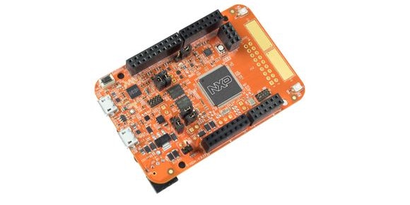
FRDM-K82F: A Freedom board with a 100LQFP K82 device. Also includes dual QuadSPI, touch pad, Arduino compatible footprint, and FlexIO header compatible with OV7670 camera.
TWR-K80F150M: A Tower board with 121XFBGA K80 device. Includes dual QuadSPI, SDRAM, EVMSIM, SDCard holder, touch pads, and more.
TWR-POS-K81: A Point of Sale reference design board in tower form factor. This board is only available via your NXP sales representative.
The K8x MCU Family Hardware Tools selection guide has more details on board differences.
Where can I find more information on the bootloader that comes built into the silicon of the K8x family?
Download the K80 Bootloader Tools package.
If interested in QuadSPI, the Kinetis Bootloader QuadSPI User's Guide that comes as part of that package describes all the steps needed to get up and running with QuadSPI.
The other information found on the Kinetis Bootloader website is also useful as this is what the ROM Bootloader is based off of.
What interfaces does the ROM Bootloader support?
The ROM Bootloader on the K8x family can interface via LPUART, I2C, SPI, or USB HID (via BLHost) to erase and program both the internal flash and/or QuadSPI flash. This is the same bootloader found on other Kinetis devices, but also includes some more advanced features to support QuadSPI.
How can I enter bootloader mode?
By default, when using a Kinetis SDK project, the bootloader is disabled and the code immediately jumps to the address in Flash pointed at location 0x4.
By asserting the NMI pin at reset though, the part can be forced to enter bootloader mode. This is useful for programming the QuadSPI or interfacing with the bootloader in other ways. This feature is controlled via the FOPT[BOOTPIN_OPT] bit, which the Kinetis SDK code sets to '0' to enable the NMI pin to enter bootloader mode.
The NMI button on each board is:
FRDM-K82F: SW2
TWR-K80F150M: SW2
The FOPT register (at 0x40C) can be modified to always go into Bootloader mode if desired. Details are in boot chapter of the K80 reference manual.
Where is the bootloader configuration data found in Kinetis SDK?
The Bootloader Configuration Area (BCA), which begins at address 0x3C0, is defined in C:\Freescale\KSDK_1.3.0\platform\devices\MK80F25615\startup\system_MK80F25615.c starting on line 133. You must also add the define BOOTLOADER_CONFIG in the project settings to let the linker files know to program this BCA area.
The FOPT configuration register (at 0x40D) is defined in C:\Freescale\KSDK_1.3.0_K82\platform\devices\MK82F25615\startup\<compiler>\startup_MK80F25615.s and by default is set to 0x3D which disables the bootloader, but does enable the option to enter bootloader via the NMI pin at reset (see previous question)
How can I use the UART port on the FRDM-K82F with the BootROM?
The OpenSDA/UART lines on the FRDM-K82F use LPUART4, which is not used by the BootROM. If you would like to use the serial UART lines to interact with the BootROM, you can blue wire a connection from either J24 or J1, and connect to R32 (RX) and R36 (TX). This was due to muxing trade-offs.
The OpenSDA/UART lines on the TWR-K80F150M are connected to UART1 and thus no modification is necessary for that board.
Also keep in mind that you can use the USB interface with the BLHost tool on both boards with no modification.
The examples in Kinetis SDK setup the QuadSPI Configuration Block (QCB) data using a qspi_config.bin file. How can I generate my own custom QCB file?
There is a C file that come as part of Kinetis SDK (C:\Freescale\KSDK_1.3.0\examples\twrk80f150m\demo_apps\hello_world_qspi\qspi_config_block_generator.c) or in the KBoot zip file, that can be compiled with various toolchains on a host computer, that will then produce a .bin file. You could import this file, and then after compilation, run it, and it will write out the new .bin to your hard drive.
There is a tool under development that simplifies this process by reading in that example .bin file and then you can modify the fields in the app, and then it will write out the modified .bin file.
Can I jump directly to QuadSPI for Execute in Place (XiP) after booting?
Yes. However note that you must still put the Bootloader Configuration Area (BCA) into internal flash. And you also may want to put the QuadSPI Configuration Block (QCB) in flash as well since it needs to be read before the QuadSPI is setup. Thus even if all your code is in QuadSPI address space, the internal flash must also be written at least once to put in the configuration data. Once you have that set though, then you can develop code by only programming the QuadSPI address space.
Where can I find instructions and details on the hardware used to evaluate the K8x family?
FRDM-K82F: http://nxp.com/frdm-k82f/startnow
TWR-K80F150M: http://nxp.com/twr-k80f150m/startnow
Which version of Kinetis SDK supports the K8x family?
Kinetis Software Development Kit (KSDK) support is split depending on the evaluation platform.
For TWR-K80F150M, support can be found in the Kinetis SDK 1.3 Mainline Release.
For FRDM-K82F, support can be found in the Kinetis SDK FRDM-K82F Stand-alone release.
Note that the FRDM-K82 standalone release is truly standalone, and does not require the mainline release to be installed.
How do I run the FRDM-K82F OV7670 camera demo?
See this Community post: https://community.freescale.com/docs/DOC-329438
How can I use the micro SD card reader on the TWR-K80F150M?
Because the SD card signals are shared with the QuadSPI signals, the SD card slot is not connected by default. See section 3.14 of the TWR-K80F150M User Guide for details on how to connect it, with the understanding that QuadSPI will not be available on the board while using SDHC.
How do I use the SDRAM on the TWR-K80F150M?
See section 3.9 of the TWR-K80F150M User Guide. Due to the layout of the board, the OpenSDA UART feature cannot be used while running the SDRAM as jumpers J6 and J8 need to be removed.
I’m having debugger connection issues when using an external debugger, like a Segger JLink. Why?
It’s likely that the OpenSDA circuit is interfering, and thus needs to be isolated via jumpers on the board.
For TWR-K80F150M: Pull J16 and J17
For FRDM-K82F: Pull J6 and J7
Also make sure you are using the correct debug header for the K8x device on the board:
For TWR-K80F150M: J11
For FRDM-K82F: J19
Where is the CMSIS-DAP/OpenOCD debug configuration for the K8x family in Kinetis Design Studio?
KDS 3.0 does not support programming the K8x family via the CMSIS-DAP interface. You will need to change the OpenSDA app on the board to either J-Link or P&E as described in the K8x Getting Started guides (Part 3).
I can't get OpenSDA on the FRDM-K82F into bootloader mode.
Make sure jumper J23 is on pins 1-2 to connect the reset signal to the OpenSDA circuit. On some early versions of the board this was incorrectly installed on pins 2-3 instead.
When using IAR with the default CMSIS-DAP debug interface, I sometimes get the error: “Fatal error: CPU did not power up”
This is an issue in some older versions of IAR. Upgrade to at least version 7.40.5 which fixes this.
When using KDS with the JLink interface with the FRDM-K82F board, I get an error.
If you see the error "The selected device 'MK82FN256XXX15' is unknown to this version of the J-Link software." it's because the J-Link driver that comes with KDS 3.0.0 does not know about the K82 family. You can either select a MK80FN256XXX15 device (which is compatible with the K82 on the board) or update the JLink software by downloading and installing the latest JLink Software and documentation pack. At the end of the installation process it will ask to update the DLLs used by the IDEs installed on your computer, so make sure to check the KDS checkbox on that screen.
I’m using the P&E OpenSDA App and debugging is not working. I get either "Error reading data from OpenSDA hardware. E17925" or “The system tried to join a drive to a directory on a joined drive” in KDS
If using IAR, make sure you have the latest version (7.40.7 or later)
The FlexIO module was first introduced in the Freescale Kinetis KL43 family. It is capable of emulating various serial communication protocols including: UART, SPI and I2C. The FlexIO module is very flexible and you can configure it according to your communication needs. The main components of the FlexIO module are the shifters, timers, and pins. Data is loaded onto a shifter and a timer is assigned to generate the shifter clock and use a pin to output the data from the shifter.
The KL43 FlexIO module has 4 32-bit shifters, 4 16-bit timers and 8 bidirectional I/O pins. Each shifter and timer has its own configuration registers. The most important registers that configure the whole FlexIO behavior are the SHIFTCFG, SHIFTCTL, TIMCFG, TIMCTL and TIMCMP registers. There are other registers that contain status flags, interrupt enabling bits and the buffers for the shifters.
Shifters have a timer assigned to them to generate the shift clock and it can be configured to shift data in or out. When the shifter is configured to transmit mode, the data from the SHIFTBUF register will be loaded to the shifter and the shifter status flag will be set meaning that the shifter is ready to start the transmission. In receive mode, the shifter status flag is set when SHIFTBUF has been loaded with the data from the shifter, and the status flag is cleared when the SHITBUF register is read.
The timers are highly configurable, they can use external or internal triggers to generate certain conditions to reset, enable and disable the timer. The triggers can be a timer output, shifter status flag, pin input or an external trigger input. They can be configured to enable in response to a trigger, pin or shifter condition.
Each shifter or timer can be configured to use any FlexIO pin with either polarity. The pins can be used as an input or output. A pin configured as an input for a timer can be used to receive a clock and use it as the shifter clock that is assigned to this timer.
Once everything is configured you need to read/write the shifter buffers and the shifter and timer status flags to start a transmission or to read the contents of the shifter buffer when receiving data.
The following diagram gives a high-level overview of the configuration of FlexIO timers and shifters.

Figure 1. FlexIO block diagram
In the following example configuration, the FlexIO module will be configured as a transmitter. It will use one shifter, two timers, and three pins. The pins will be used for the outputs of the shifter and the two timers. One timer will be used as the shifter clock and the other timer will be used as a chip select to show when a transmission is being made. The FlexIO will be configured to have a baud rate of FlexIO clock/4 and will do an 8-bit transmission.

Figure 2. Example transmission
Timer 0
Timer Configuration 0 Register (FLEXIO_TIMCFG0) = 0x00002200
TIMOUT = 0 Timer output is logic one when enabled and is not affected by timer reset.
TIMDEC = 0 Decrement counter on FlexIO clock, Shift clock equals Timer output.
TIMRST = 0 Timer never reset.
TIMDIS = 2 Timer disabled on Timer compare.
TIMENA = 2 Timer enabled on Trigger high.
TSTOP = 0 Stop bit is disabled.
TSTART = 0 Start bit disabled.
Timer Control 0 Register (FLEXIO_TIMCTL0) = 0x01C30101
TRGSEL = 1 Trigger select. Shifter 0 status flag.
TRGPOL = 1 Trigger active low.
TRGSRC = 1 Internal trigger selected.
PINCFG = 3 Timer pin output.
PINSEL = 1 Timer pin 1 select.
PINPOL = 0 Pin is active high.
TIMOD = 1 Dual 8-bit counters baud/bit mode.
Timer Compare 0 Register (FLEXIO_TIMCMP0) = 0x00000F01
TIMCMP = 0x00000F01
Configure 8-bit transfer with a baud rate of FlexIO clock/4. Set TIMCMP[15:8] = (number of bits x 2) - 1. Set TIMCMP[7:0] = (baud rate divider / 2) - 1.
In our case we want an 8-bit transfer so TIMCMP[15:8] = 0xF and a baud rate divider of 4 so TIMCMP[7:0] = 0x1.
Timer 1
Timer Configuration 1 Register (FLEXIO_TIMCFG1) = 0x00001100
TIMOUT = 0 Timer output is logic one when enabled and is not affected by timer reset.
TIMDEC = 0 Decrement counter on FlexIO clock, Shift clock equals Timer output.
TIMRST = 0 Timer never reset.
TIMDIS = 1 Timer disabled on Timer N-1 disable.
TIMENA = 1 Timer enabled on Timer N-1 enable.
TSTOP = 0 Stop bit is disabled.
TSTART = 0 Start bit disabled.
Timer Control 1 Register (FLEXIO_TIMCTL1) = 0x00030283
TRGSEL = 0 Trigger select. Doesn’t matter because we won’t use a trigger.
TRGPOL = 0 Trigger active high.
TRGSRC = 0 External trigger selected.
PINCFG = 3 Timer pin output.
PINSEL = 2 Timer pin 2 select.
PINPOL = 1 Pin is active low.
TIMOD = 3 Single 16-bit counter mode.
Timer Compare 1 Register (FLEXIO_TIMCMP1) = 0x0000FFFF
TIMCMP = 0x0000FFFF Never compare.
Shifter 0
Shifter Control 0 Register (FLEXIO_SHIFTCTL0)
TIMSEL = 0 Timer 0 select.
TIMPOL = 0 Shift on posedge of Shift clock.
PINCFG = 3 Shifter pin output.
PINSEL = 0 Shifter pin 0 select.
PINPOL = 0 Pin is active high.
SMOD = 2 Transmit mode. Load SHIFTBUF contents into the Shifter on expiration of the Timer.
Shifter Configuration 0 Register (FLEXIO_SHIFTCFG0)
INSRC = 0 The input source of the shifter is from a pin. In our cause this doesn’t matter because our shifter is set as transmit mode.
SSTOP = 0 Stop bit disabled.
SSTART = 0 Start bit disabled.
Once all the FlexIO components are configured you have to enable the FlexIO instance by setting the FLEXEN bit in the FLEX_CTRL register. Initially, the shifter status flag is set and is cleared each time the SHIFTBUF register is written. This flag is set each time the SHIFTBUF data has been transferred to the Shifter (SHIFTBUF is empty). The shifter status flag 0 is configured to be the trigger of the timer 0, so as soon as the status flag is cleared, the timer 0 will be enabled because TIMENA = 2 (Timer enabled on Trigger high)and TRGPOL = 1 (Trigger active low). The shifter will begin to shift out the data on the positive edge of the clock (TIMPOL = 0) until the timer is disabled. The timer will disable when the timer counter reaches 0 (TIMDIS = 2).
The timer 1 is configured to be active (low) when the timer 0 is enabled. This is because TIMDIS = 1 and TIMENA = 1. The compare register is configured to 16-bit counter and set to 0xFFFF. With this value the timer will never compare and always be active when the timer is enabled.
To send data, you have to make sure that the previous transaction was completed and you can check this by reading the TIMSTAT flag. This flag sets each time the timer counter reaches 0. Once the TIMSTAT flag is set, you clear it and write your new data to the SHITBUF register to start the transaction.
The KSDK 1.2.0 has drivers and a HAL to facilitate the configuration of the FlexIO module. Some of the important functions are:
FLEXIO_DRV_Init(uint32_t instance, const flexio_user_config_t *userConfigPtr);
Use this function to initialize the FlexIO module before using it. In this configuration you can change the settings in the FLEXIO_CTRL register such as: Doze Enable, Debug Enable, Fast Access and software reset.
FLEXIO_HAL_ConfigureTimer(FLEXIO_Type * base, uint32_t timerIdx, const flexio_timer_config_t *timerConfigPtr);
Use this function to configure a timer in the FlexIO. This function uses a configuration structure that can change the TIMCFG, TIMCTL and TIMCPM registers.
FLEXIO_HAL_ConfigureShifter(FLEXIO_Type * base, uint32_t shifterIdx, const flexio_shifter_config_t *shifterConfigPtr);
Use this function to configure a shifter in the FlexIO. This function uses a configuration structure that can change the SHIFTCFG and SHIFTCTL registers.
FLEXIO_HAL_SetShifterBuffer(FLEXIO_Type * base, uint32_t shifterIdx, uint32_t value);
Use this function to start a transmission. When writing to the SHIFTBUF register, the Shifter Status Flag is cleared.
FLEXIO_DRV_Start(uint32_t instance);
Use this function to enable the FlexIO module by setting the FLEXEN bit in the FLEX_CTRL register.
FLEXIO_HAL_GetTimerStatusFlags(FLEXIO_Type * base);
This function returns the contents of the TIMSTAT register. You can use this function to check when a transmission is finished.
FLEXIO_HAL_ClearTimerStatusFlags(FLEXIO_Type * base, uint32_t mask);
This function clears a specific Timer Status Flag. You can use this function to clear a flag after you read that the flag was set.
To change the frequency of the transmission you have to change the value of the TIMCMP register. In dual 8-bit counters baud/bit mode, the lower 8-bits configures the baud rate divider equal to (CMP[7:0] + 1) * 2 and the upper 8-bits configure the number of bits in each word equal to (CMP[15:8] + 1) / 2.
In our example the baud rate divider is set to 4, this means CMP[7:0] has the value 1. The number of bits transmitted is set to 8, this means CMP[15:8] has the value 0xF.
Let’s change the baud rate divider to 32. To obtain the CMP[7:0] value, we will have to solve the simple equation:
32 = (CMP[7:0]+1)*2
CMP[7:0] = 15=0xF
Now let’s change the number of bits to 16. The CMP[15:8] value is defined by:
16 = ((CMP[15:8]+1))/2
CMP[15:8] = 31=0x1F
The value for the TIMCMP for the timer 0 has to be 0x00001F0F to get a baud rate divider of 32 and a word length of 16 bits. The waveform will look as follows.

Figure 3. 16-bit transmission
By default the shifter in the FlexIO transmits the LSB first. To change the transmission order, you have to write to the SHIFTBUFBIS (Bit swapped) register instead of the SHIFTBUF register. There are also other buffer registers: SHIFTBUFBYS and SHIFTBUFBBS. The first register swaps the bytes and the second register swaps the bytes and bits at the same time. When using one of these registers you have to be careful to consider that the length of the SHIFTBUF registers is of 32 bits, so if you choose to use the SHIFTBUFBIS for a transmission and your transmission length is not of 32 bits, you have to start writing your data starting from the most significant bit.
The following image shows a MSB transmission. The value 0x6AED0000 was written to the SHIFTBUFBIS register.

Figure 4. MSB 16-bit transmission
The FlexIO module supports automatic start and stop bit handling. All you have to do is change the SHIFTCFG and the TIMCFG configuration bits. In the SHIFTCFG register set SSTOP to 11 if you want the stop bit to have the value 1, and set the SSTART to 10 if you want the stop bit to have the value 0. In the TIMCFG register set the TSART to 1 and the TSOP to 10.
The transmission will look as the following image. Data transmitted 0x0F.

Figure 5. Transmission with start and stop bit
Changing the phase of the clock is very easy, you just have to set the TIMPOL bit to 1 in the SHIFTCTL register.

Figure 6. Shift on negedge of Shift clock
The conditions to disable and enable the timers can be configured by changing the TIMENA and TIMDIS values in the TIMCFG register. In our example the timer is enabled by the trigger high. The trigger can be set to be an external pin, a shifter status flag, or a timer output. In our case the trigger was set to the shifter status flag, but you can change this configuration to your communication needs. The timer can also be enabled when the previous timer is enabled, on a certain pin edge, or with a combination of pins and triggers.
The timer in the example above disables on the timer compare. This means that when the timer counter reaches zero, the timer will disable automatically. The timer counter is loaded with the timer compare value every time it reaches zero or when it is first enabled. The timer can also be disabled by other conditions such as: when the previous timer is disabled, on a trigger falling edge, on a pin edge, or on a combination of these.
Each pin can be configured to be active high or low. When a pin polarity is changed it only affects the output of the pin, for example, if a timer is set to be the shifter clock and you change the pin polarity, the shifter clock will not change its polarity, only the output to the pin from the timer will change.
The configuration for the polarity of the pins is located in the TIMCTL and SHIFTCTL. When the PINPOL value is changed to 1, the pin is active low. In the following image the polarity of the timer pin and the shifter pin was changed to 1, so they are active low.

Figure 7. Timer and Shifter active low
The FlexIO module can generate an interrupt from 3 sources: Shifter error, Shifter status flag and Timer status flag. To enable the interrupts you need to set the bits in the SHIFTSIEN,SHIFTEIEN and TIMIEN.
If you are using KSDK you can enable the interrupt in NVIC by setting true .useInt in the FlexIO user config that the function FLEXIO_DRV_Init utilizes. The default handler for the interruption is named UART2_FLEXIO_IRQHandler.
The following example configuration will configure the FlexIO module as a receiver. This configuration works with the first example configuration shown. Both tower boards (TWR-KL43Z48M) have to be connected as shown further below in the Table 1 Hardware connnections. The FlexIO module will use one Shifter, one timer, and three pins. The pins will be used for the input of the shifter, the input clock for the timer and the trigger for the timer. The timer will use pin 1 as an input and its output will be the same as the input clock. The trigger for the timer will be the transmitter chip select pin and it will be used to enable or disable the timer. The FlexIO will be configured to do an 8-bit transmission.
Shifter 0
Shifter Control 0 Register (FLEXIO_SHIFTCTL0) = 0x00800001
TIMSEL = 0 Timer 0 select.
TIMPOL = 1 Shift on negedge of Shift clock.
PINCFG = 0 Shifter pin output disabled.
PINSEL = 0 Shifter pin 0 select.
PINPOL = 0 Pin is active high.
SMOD = 1 Receive mode. Captures the current Shifter content into the SHIFTBUF on expiration of the Timer.
Shifter Configuration 0 Register (FLEXIO_SHIFTCFG0) = 0x00000000
INSRC = 0 The input source of the shifter is from a pin. In our cause this doesn’t matter because our shifter is set as transmit mode.
SSTOP = 0 Stop bit disabled.
SSTART = 0 Start bit disabled.
Timer 0
Timer Configuration 0 Register (FLEXIO_TIMCFG0) = 0x01206602
TIMOUT = 1 Timer output is logic zero when enabled and is not affected by timer reset.
TIMDEC = 2 Decrement counter on Pin input (both edges), Shift clock equals Pin input.
TIMRST = 0 Timer never reset.
TIMDIS = 6 Timer disabled on Trigger rising edge.
TIMENA = 6 Timer enabled on Trigger falling edge.
TSTOP = 0 Stop bit is disabled.
TSTART = 1 Start bit enabled.
Timer Control 0 Register (FLEXIO_TIMCTL0) = 0x04C00103
TRGSEL = 4 Trigger select. Pin 2 input.
TRGPOL = 1 Trigger active low.
TRGSRC = 1 Internal trigger selected.
PINCFG = 0 Timer pin output disabled.
PINSEL = 1 Timer pin 1 select.
PINPOL = 0 Pin is active high.
TIMOD = 3 Single 16-bit counter mode.
Timer Compare 0 Register (FLEXIO_TIMCMP0) = 0x0000000F
TIMCMP = 0x0000000F Configure 8-bit transfer. Set TIMCMP = (number of bits x 2) - 1.
The shifter status flag is set every time the SHIFTBUF register has been loaded with data from the shifter. This occurs every time that the transmitter sends 8 bits of data. You can read the shifter status flag by polling or by enabling an interrupt based on your needs. This flag clears automatically when you read the SHITBUF register.
During the transmission, the first thing that happens is that timer from the receiver will be enabled because the chip select signal from the transmitter is configured as a trigger. Once the timer is enabled, the timer will begin to decrement on the pin input, this means that the shifter clock of the receiver will be equal to the pin input. The transmitter shifter is configured to shift data out on the positive edge of the clock and the receiver shifter is configured to shift data in on the negative edge of the clock. After 8 bits have been transmitted, the compare register from the receiver will reach 0 and this generates an event to store the data from the shifter to the SHITBUF register and the Shifter Status Flag will be set. Finally the timer will be disabled by the chip select signal and keep waiting for another transaction.
The hardware connections are shown in the following table.
Signal name
TWR-KL43Z48M transmitter
TWR-KL43Z48M receiver
Pin name
Board Location
Pin name
Board Location
Serial Data
PTD0/FXIO0_D0
B46
PTD0/FXIO0_D0
B46
Clock
PTD1/FXIO0_D1
B48
PTD1/FXIO0_D1
B48
Chip Select
PTD2/FXIO0_D2
B45
PTD2/FXIO0_D2
B45
GND
GND
B2
GND
B2
Table 1. Hardware connections

Figure 8. Hardware connections
The example projects for the FlexIO transmitter and receiver are developed in KDS 3.0.0 with KSDK 1.2.0. The application lets the user communicate with the transmitter via a serial terminal and the transmitter sends each character to the receiver via FlexIO and the receiver displays the received character on another serial terminal.
To be able to compile the project, first you need to compile the library located in C:\Freescale\KSDK_1.2.0\lib\ksdk_platform_lib\kds\KL43Z4.
Once the two TWR-KL43Z48M are connected as described above, import both projects into KDS, compile the platform library, and both projects. Open two serial terminals configured to 115200 bauds and run each project on a different tower.
On the transmitter terminal you can write anything and it will be displayed and transmitted to the receiver tower via FlexIO and will be shown on the other terminal.

Figure 9. FlexIO example application. Transmitter (left terminal). Receiver (Right terminal).
The FlexIO module is also capable of generating a PWM signal by configuring one of its timers to the Dual 8-bit counters PWM mode. This mode is configured by writing 01 to TIMOD in the TIMCTL register. In this mode, the lower 8-bits of the counter and compare register are used to configure the high period of the timer output and the upper 8-bits are used to configure the low period of the timer output. The shifter bit count is configured using another timer or external signal.
To calculate the frequency of the PWM signal you have to add the lower 8-bits of the counter and the upper 8-bits and divide it by the FlexIO clock*2 (Only if the timer is configured to decrement on the FlexIO clock.)
The frequency of the PWM signal is given by:
f = (FlexIO clock)/(TIMCMP[15:8]+TIMCPM[7:0]+2)
To calculate the TIMCMP values to get a certain frequency you can solve the equation for TIMCMP
TIMCMP[15:8]+TIMCPM[7:0] = (FlexIO clock)/f-2
For example, let’s say we want a 200kHz PWM signal, by using the formula above and using the FlexIO clock of 48MHz, we get that the sum of the TIMCMP values must be 238. If we want a 50% duty cycle we need to write the value 238/2 to the lower and upper 8 bits of the TIMCMP register.
The waveform generated by these settings is shown in the figure below.

Figure 10. 200kHz 50% duty cycle PWM signal
To change the duty cycle you need to change the values of TIMCPM[15:8] and TIMCPM[7:0] but without changing the sum of both values, otherwise the frequency will also be altered. For example, if we need a 20% duty cycle we multiply 0.20*238 and 0.8*238. We round up the results and get TIMCPM[7:0] = 48 and TIMCPM[15:8] = 190. The waveform generated will look as shown in the figure below.

Figure 11. 200kHz 20% duty cycle PWM signal
The above steps are in the attached video 'Kinetis SDK V2.0 Configuration Generation.mp4'
Installing Kinetis SDK v2.0 New Project Wizard in Kinetis Design Studio

See attached video 'Installing KSDK v2.0 Project Wizard in KDS.wmv'
For offline installation: the wizard can be downloaded from the https://www.nxp.com/kds web site under the Kinetis Design Studio V3.0.0 downloads, e.g. for Windows it is here:

Creating and Debugging KSDK V2.0 Project
Steps are shown in the attached video 'Create build and debug Kinetis SDK v2.0 project.wmv'
Links:
- Kinetis SDK: Welcome to Kinetis Expert | Kinetis Expert
- Kinetis Design Studio: Kinetis Design Studio Integrated Development |NXP
What is QuadSPI Flash? Why should I use it?
QuadSPI is a name for a popular type of serial NOR flash memory that is SPI compatible, but also allows for multiple data lines (up to 4 per device, or 8 if done in parallel) with bi-directional data for increased memory bandwidth. The QuadSPI controller on the K8x also allows for Execute-In-Place (XIP) mode so that code can be executed out of this external memory. QuadSPI memory can be used for either extra memory storage or for extra code space, or a combination of both. After initialization, it appears as a readable area of memory starting at 0x6800_0000 (as well as at the alias regions).
How can I program the QuadSPI?
There is an example application in Kinetis SDK that shows how to program the QuadSPI at C:\Freescale\KSDK_1.3.0\examples\twrk80f150m\driver_examples\qspi
For programming an entire application, the ROM bootloader can be used. Details are in the K80 Bootloader Tools Package.
The Kinetis Bootloader QuadSPI User's Guide that comes as part of that package describes all the steps needed to get up and running with QuadSPI. There is also an example Kinetis SDK application that runs out of QuadSPI at C:\Freescale\KSDK_1.3.0\examples\twrk80f150m\demo_apps\hello_world_qspi_alias
What performance tips are there if doing QuadSPI XIP?
A few key performance factors:
- Ensure both the data and instruction cache is enabled
- Use as many data lines as possible (4, or 8 if available in dual/octal modes)
- Use DDR mode
- Any critical code should be placed in Flash/RAM for fastest performance
- If using XIP, code should be executed out of the QuadSPI aliased address space which starts at 0x0400_0000.
A more detailed app note is under development.
How do I debug code located in QuadSPI?
You must make use of the aliased QuadSPI address space at 0x0400_0000. There is an example of this in the hello_world_qspi_alias example in Kinetis SDK. Due to the architecture of the M4 core on Kinetis, breakpoints cannot be set in the 6800_0000 address space, which is why the alias address space is provided.
What app notes are available for the QuadSPI?
Because the QuadSPI module found on the K8x family has also been used on other NXP devices, there are some app notes available that can be useful for QuadSPI development. Note that some of the implementation details and features as described in the app notes will be different for K8x, so please use the K8x reference manual for full details.
Couldn't find an answer to your question? Email us.