(This project is being managed here: Project Repository )
Introduction:A continuity testing device is used to check the breakage and shortage of wires in a circuit. Sometimes in a complex circuit design, we are unaware of the fault so we have to test the circuit at every point to find the real problem. This plays an important role in designing of the electric circuit. It is always a good practice to verify continuity in a circuit before implementing it. In electric circuits, we use conventional bulky meters to check the continuity of a circuit. While working in a field, it is not possible to carry a bulky meter with the circuit. Here is a PCB device with a compact size of board and components on it that can check the continuity as well as the polarity of the components like diodes, Zener diodes, LEDs etc. It is important to place the components in right polarities otherwise placing the components in opposite polarities can damage the whole circuitry. You can carry it easily in your packet and can test your circuit anywhere.
Checking polarity of a transistor with a conventional meter
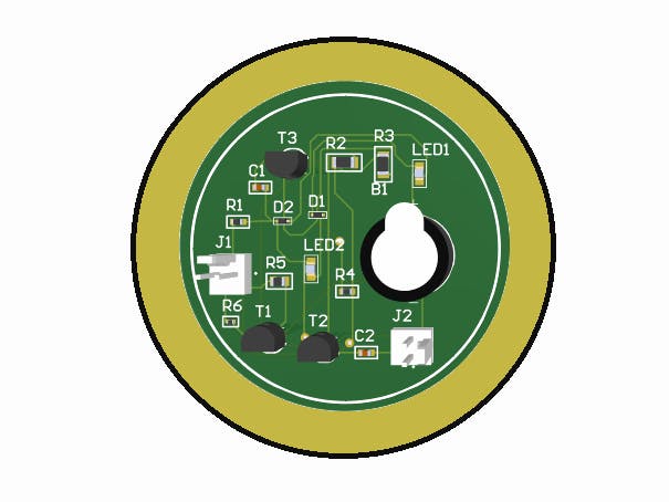
When you connect the component which you want to test with the PCB device continuity tester, both the LED will glow showing the activation of the circuit. There are two LEDs in a board performing different function[s separately. LED1 will glow only when the wire of the circuit is connected to the cathode terminal of the diode.
There are two transistors connected in the circuit which are not in phase with each other. This means that if one transistor will give high output then the other will give low output and vice versa. First LED will turn on when transistor one is on and second LED will turn on when the second transistor will turn on keeping the other low. When the component is placed between the wires to test the polarity it bypasses to the LED depending on the polarity as a result the current will start flowing current through the circuit. If no LED will glow this will identify that there is a short circuit at some place in a circuit.
If the component is placed in a right polarity, then by placing the probes across the component in a circuit will sound the buzzer alarm. This will indicate that the circuit is in working condition or perfectly alright to implement. Using this PCB device you can check different types of circuits and components.
Schematic Diagram:I have implemented the design on Altium designer. I have designed symbols and footprints for each component then I uploaded my symbols and footprints libraries online on Inventhub where users can view, download, or use them. Users do not need to design the components for their design. Thus, it can save time.
After completing the design of components. I have used them in my schematic to complete my design. I have uploaded my schematic file for the users and viewers on Inventhub.
PCB Design:After designing schematic, I have converted my schematic file to the PCB file so that I can design a board, connect my components, and can visually view my board in 3D. I have uploaded my PCB file on Inventhub where the manufacturer can view or download my PCB file for the fabrication.
Design for Manufacturing:For the manufacturer, I have created a release of my project which contains all design files including schematic, PCB, and their component libraries. Instead of visiting my manufacturer, I can send him the release of my design files. He can view or download files in ZIP format and can fabricate my PCB without any errors.
Bill of Materials:After getting my fabricated board, I need to embed components on it. I have created a BOM file on Inventhub which contains library reference, footprint, and quantity of each component. My component provider can simply download the file in CSV format and can send my components. I can calculate the total cost of my design by selecting the ‘supply chain’ option. I can select my distributor for the components depending on the price and availability of the components. Our total cost is $7.43.
Feel free to ask queries at arshmah@inventhub.io


Comments