

Hardware components | ||||||
| × | 1 | ||||
 |
| × | 1 | |||
| × | 1 | ||||
Software apps and online services | ||||||
 |
| |||||
| ||||||
This laboratory exercise explored the practical use of a Digital-to-Analog Converter (DAC) to generate various continuous electrical signals. By connecting an RT-Spark Development Board to a digital oscilloscope, the physical behaviors of digital signal generation were observed in real-time. The primary objective was to generate, visualize, and analyze square, ramp, and sine waves. This activity provided a foundational understanding of how microcontrollers translate discrete digital data into measurable analog voltages.
2. Design and TestingThe execution of the experiment required a combination of precise hardware wiring and software configuration to successfully produce and measure the required waveforms.
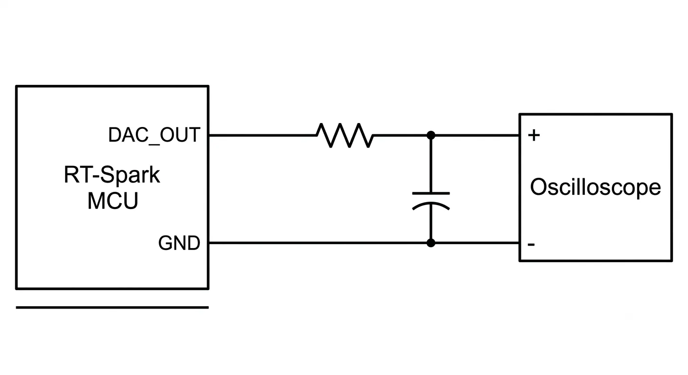
Hardware Configuration The main device utilized was the RT-Thread RT-Spark Development Board, which contains an ARM-based STM32 microcontroller. To visualize the signals, a digital oscilloscope was connected directly to the development board. The positive probe of the oscilloscope was attached to the DAC_OUT pin to capture the signal output, while the ground clip was attached to the GND pin to provide a stable common reference point.
Software Configuration The software environment relied on STM32CubeIDE and STM32CubeMX. The shape of the waveform was controlled by modifying a specific parameter within the main program loop. By changing the final parameter in the tone_play function to SQUARE, RAMP, or SINE, the microcontroller was instructed to output the corresponding signal shapes. The updated code was then compiled and downloaded to the board for observation.
Measurements and visual observations were carefully recorded for the three generated waveforms using the digital oscilloscope. A notable difficulty encountered during this phase was operating the oscilloscope to extract accurate readings. Locating the exact signal measurements required careful navigation of the equipment's measurement menus and precise adjustments to the screen's time scale, which initially proved to be a challenging but valuable learning experience.
3.1 Square Wave Analysis The system was first configured to output a square wave. The following electrical characteristics were successfully extracted from the oscilloscope display:
The rise and fall times of 800 nanoseconds reflect the brief physical settling time required by the DAC to transition between logic states. The 0.133-millisecond period confirms that the wave was operating at a frequency of approximately 7.5 kHz.
3.2 Ramp Wave Analysis When the software was adjusted to output a ramp wave, the rising edge of the signal appeared jagged rather than perfectly smooth.
- Cause of the Jagged Edge: This visual stepping is caused by the DAC's 8-bit resolution. An 8-bit system can only output 256 distinct voltage levels. Therefore, instead of a smooth, continuous slope, the voltage increases in tiny, discrete steps, creating a "staircase" visual effect.
- Hardware Smoothing: To smooth this jagged edge physically, a low-pass RC filter (composed of a resistor and a capacitor) can be wired to the DAC output to blend the sharp voltage jumps together.
- Software Smoothing: To achieve a smoother wave purely through coding, the DAC update rate can be increased while using smaller voltage increments per step. This minimizes the size of the "stairs, " making the wave appear more continuous.
3.3 Sine Wave Analysis The final test involved generating a continuous sine wave. Through software experimentation, it was determined that the absolute maximum frequency sine wave that the microcontroller's loop could generate was 15, 625 Hz.
The laboratory exercise successfully demonstrated the practical application of digital-to-analog conversion. While setting up the software and hardware was straightforward, extracting precise data proved to be a significant part of the learning curve. Navigating the digital oscilloscope to find exact values—especially the nanosecond transition times—was initially difficult but ultimately highlighted the importance of using proper measurement tools in electronics. Furthermore, observing the jagged edges of the ramp wave provided a clear, real-world visual of digital quantization limits. Overall, the activity reinforced key concepts in firmware programming, electronic signal analysis, and proper laboratory documentation.


Comments