

Hardware components | ||||||
 |
| × | 1 | |||
 |
| × | 1 | |||
Software apps and online services | ||||||
 |
| |||||
This project was first published as a 3 part blog on Planet Analog in May 2016.
Part 1: Signal AcquisitionIntroductionHands up all who remember I did a blog on measuring the RMS (root mean square) value of a signal. Hmmm. Nobody! Well for those of you who don’t believe that I wrote one you can find it here: RMS Measurement. In that blog I described different methods that could be used, but I omitted the possible approach where the RMS value is generated using hardware for the mathematics. You could use a Digital Signal Processor (DSP) or an FPGA. I an unfamiliar with both, but as I have become more familiar with the PSoC family the thought niggled at me that perhaps I could create an RMS measurement completely within a PSoC5 device.
For those of you unfamiliar with the PSoC concept from Cypress, the device provides a microcontroller plus hardware blocks to create your own peripheral set. These peripherals are known as “components” and each component in fact comes with its own data sheet. The concept extends across digital and analog functionality. It may not have the granularity of an FPGA, but the approach can generate some very versatile designs. Full disclosure: I am not, nor have I ever been employed by Cypress or its representatives and distributors, but my employer is a part of the Cypress Design Partner program.
Let’s start out with a little background of how I am going to adapt the mathematics to get to a result. The RMS value of a signal is given by the equation:
If we work with discrete measurements and for simplicity let’s work with t0=0 we can approximate and sum the measurements as follows:
Where Δt is the sample time and N is the number of samples. Conveniently the Δt cancels out and we are left with
In other words we take N samples, judiciously timed to include a full cycle exactly (technically you can of course go beyond that), sum the squares of the readings and divide by the number of readings- and then take the square root. That’s pretty much the way it is done in software as well.
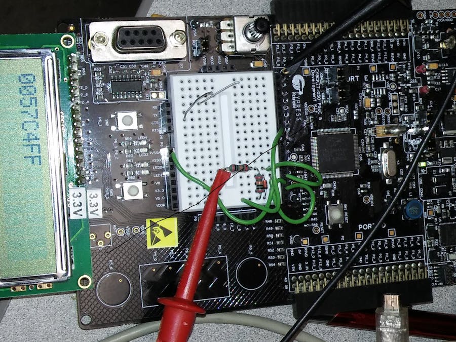
This series of blogs follows the signal path, which means I have the advantage of hindsight as to what problems there were and the actions I took to solve them. I certainly didn’t develop the concept linearly. I really needed to figure out how to realize the more complicated parts before I knew if the idea was viable. I was fortunate to have a CY8CKIT-050 PSoC 5LP development kit (using a CY8C5868AXI-LP035 device) along with a MiniProg3 debugger. I am indebted to the folks at Cypress Tech Support, especially Sujay Yadawadkar and Erik Schembor for their excellent support as I built this concept.
You can find my PSoC Creator project here. Please be aware that because of a minor bug (detail to come in my second blog) in PSoC Creator version 3.3 it is better to work with Creator 3.2 or earlier. I developed this with PSoC Creator 3.1SP3. If you are going to open my project you will need to download the Square Root component before you will be able to generate and compile the project without an error. I will describe how to do that that in my third blog on the square root generation.
Signal InputThe first thing to note is that in generating the RMS value, the input signal is squared, so there are no negative numbers and for a single supply device this translates to the possibility of using a full wave rectifier. Of course you might just go for a bridge rectifier, but there are the voltage drops due to the diodes and the zero is offset from ground.
I did find a Cypress app-note loose on the web on making a precision rectifier using the mixer component, but as I tried to implement it I found that there is no AN59649 on the Cypress web site and that description does not match the mixer component, so obviously the promising concept did not really bear fruit. That means I had to resort to a simple precision rectifier using an op-amp, of which there are many examples on the web. I appropriated a circuit from Linear Technologies (also in Microchip’s AN1353) which allows for rectifying a bipolar signal with a single supply op-amp. This is the circuit that appears in Figure 1-1.
Figure 1
Implementing this on a PSoC is straightforward using its op-amp component. I did find a 95mV differential in the peak value between input and output for a sine wave, and the difference for a triangular wav was imperceptible. The output signal started clipping at 5.85Vp-p on a device powered at 3.3VDC.
The rectified signal is connected to an analog to digital converter (ADC) as shown in Figure 1-2.The ADC is configured to initiate a conversion according to an external signal that is derived from a clock that is 16 times the frequency of the incoming analog signal. This is one of those cases where my choice of 16 samples is described later.
Figure 2
The ADC can be configured as 8, 10 or 12 bit converter, but that is just for the software API (Application Programming Interface) provided. The conversion is always 12 bits and the DMA access is always 16 bits. Transfer to the next stage of our RMS measurement is via DMA, but you may do better to insert a hold in the logical sequence. The next blog will deal with the squaring of the data, but it is easier to work with preprogrammed constant data rather than with the vagaries of a continuously changing ADC output. The approach in this blog has been rather conventional. Hold onto your hats for the Digital Frequency Block.
Part 2: Squaring a ReadingIn the first part of this series, Measuring an RMS value on a PSoC5, Part 1: Signal Acquisition, I described the way to rectify the incoming signal and how to connect up the ADC (analog to digital converter). The next step in generating the RMS value is to square the readings and accumulate them. We need to descend an abstraction level to understand how to do that.
One of the reasons that I was interested in this project was that I wanted to delve deeper into the workings of the PSoC. Cypress has allowed users to create their own components using Verilog or a technique called “datapaths” and so I girded myself to create this project using those techniques. As I poked around I came across some components created by the PSoC community (data sheet) and in there I found an “Integer Square Root Calculator” as well as “Multiply and Accumulate using the DFB”.
All my plans for learning Verilog went out the window. I went through the datasheet of the latter and decided that it wouldn’t quite meet my needs. However it held promise, for not only would it square the input, it would accumulate the squares as well which is exactly what I needed. The data sheet for the Multiply and Accumulate component spoke about “Q23” formatted numbers (which didn’t mean much to me at the time) and seemed to preclude the general number multiplication that I wanted. It also posed a problem as to how to write the same number twice to get the square. But I thought I could tweak the design to my own needs. “Tweak” was not quite the word.
According to the DFB (Digital Filter Block) datasheet, the “Digital Filter Block is a 24-bit fixed-point, programmable limited-scope DSP with a 24*24 Multiply and Accumulate Unit (MAC), a multifunction Arithmetic Logic Unit (ALU), and data routing, shifting, holding, and rounding functions.” That’s a mouthful, but sounds simple enough. I was amazed a quite how convoluted the design is. I googled for “DFB”s in the FPGA realm, but nothing came anywhere as complex as this.
The first movie I ever saw at a drive-in theatre was “The Five Pennies” with Danny Kaye and Louis Armstrong. One of the songs that stuck with me is called “The Music Goes Round and Round”. I suggest you listen to it before continuing to get a flavor of what I was feeling. Each time I read the data sheet all I could think was “the data goes round and round and it comes out there” and then I would point at hold registers at the output. Figure 2-1 gives you a partial view of the structure.
I could write (and originally did before I edited it down) several blogs just on the issues and problems of the DFB datasheet. Let me just quote Cypress FAE Frank Kees (DFB assembler and (Significantly) Improved Simulator component):
“We were doing some development with the DFB and came to realize what a frustrating experience it was to learn and program the DFB. The documentation needs a significant overhaul, but in the meantime, a much better simulator was an absolute must…”
As far as I can tell the DFB documentation has not been yet upgraded. But since I managed to get it working in the end, let me move on.
The first issue was that on PSoC Creator version 3.3, portions of the simulator window for the DFB module are somehow visually stretched to the point of being unusable. I am told the version 3.2 does not have the problem, but I developed on Creator version 3.1 SP3 which definitely worked. Components get modified as Creator evolves. You may be prompted to replace the components. As long as you don’t want to go back to an earlier revision of Creator it is fine to continue with the replacement.
Once you start working with the code for the DFB let me give you an important hint: always and frequently click on the “Apply” or “OK” buttons at the bottom of the window. Using the “X” at the upper right to close the window may lose you a lot of work (and yes, I speak from bitter experience) since there is no confirmation required for this action, even if something has changed.
Figure 1
The DFB works with a Very Long Instruction Word (VLIW) format. Each word comprises of instructions for the four elements of the DFB: the multiplexers, the ACU (address Calculation Unit), the ALU (Arithmetic Logic Unit) and the MAC (Multiplier/Accumulator) with a few modifiers (my word) that include jumps, shifts, writes and input register selection. The ALU has pipelining to add to the complexity. It’s just like assembly programming but much more primitive. For instance there is no way that I can see for a loop counter, and it has some arcane rules- like a label must be preceded by a jump instruction, no doubt something to do with the state machine that encapsulates the code.
The whole DFB works on 24 bits of data (including a sign bit), but multiplying two numbers together you get 48 bits of data including the sign bit. However it is only possible to access the upper 24 bits of data. (The data is formatted as “Q23” at the input and “Q1.22” at the output (see here for some information of the Q number format), but we can sort of ignore that.) At the suggestion of Cypress tech support, I discovered that I could multiply two 12 bit numbers and still get an accessible result if I increase my 12 bit input by a factor so that when multiplied, the results would be in the upper 24 bits. Obviously the results would have to be adjusted to compensate for that factor.
In order for a squared number to show up in the least significant bit of the upper 24 bits (bit 224) the least significant bit of the number would be 212i.e. the square root of 224. That means I would have to shift the incoming data 12 times so that the least significant bit of my input would appear at the 12th bit location to make it into the calculation result. Squaring a 12 bit number would result in a 24 bit number and so it was apparent that I would have to be satisfied with less than a 12 bit number. But it gets a bit more complex because aside from the sign bit, there is also the accumulation of the squares and that will also increase the number of bits in the answer. I came to a compromise to use a 9 bit value as an input and 16 samples that would translate into a ((9 x 2)+4=) 22 bit result.
Based on this analysis I had to shift the incoming 12 bit number 9 times so that the d3 of the incoming data ends up at d12 of the data that will be squared. The least significant three bits would be truncated, well almost. The result however will be a little better than 18 bits though, because the lesser bits still form part of the multiplication and the carries will pass on up.
Figure 2
The code is shown in Figure 2, right side. Note that there are several “NOP”s and dummy steps to allow for the pipelining of the DFB. One of the limitations of the shift function of the ALU is that it only allows left shifts of one or two positions, so to get to nine needed some thought. I started off by clearing the accumulator in the MAC (lines 4 and 5). I wanted a complete clear MAC and since the MAC(clra) instruction actually causes a multiplication I used this alternate approach.
Once the data is received (line 25) from a DMA transfer in, the input data is passed to the ALU output. I then shift the ALU output twice and store it to RAM-A (line 31)- it could just as easily been RAM-B. That RAM data is then passed to the ALU output (line 34). The ALU output is again shifted twice and then written back to RAM-A (line 40). This sequence is repeated twice more and then once more with the data being shifted once instead of twice for a total of 9 shifts. The 9 times shifted result is also stored into RAM-B. To me it would be logical that once you had shifted data it would remain in the shifted state, but this is not the case, so there has to be a shift (line 50) to write to RAM-B as well the original write to RAM-A (line 48).
See what I mean-
The data goes round and round o-o-o-o…
The contents in RAM-A and RAM-B (the same number) are passed to the MAC and multiplied to get the square (line 56). The actual result is shifted left by one (appearing to be multiplied by 2), apparently as a result of the number formatting.
And it comes out squared!
For each subsequent input number, it is squared and added to the number in the accumulator and retained there. After 16 such calculations I want to output the accumulated total and clear the MAC. I managed to do that using an external counter (I will get to that) but trying to figure out how to conditionally jump in the DFB code based on the inputs is yet another exercise in frustration as the inputs to the module are sometimes called “interrupts” or “global inputs” or “in_1” and there is not really an explicit conditional test. The DFB will not execute a jump if the input is not set (under the right conditions- a certain flag must be set to enable this feature see thealu(englogbals,001) in line 58) as you can see in line 64.
When the input signal is low (the sense is inverted externally) the jump in line 64 is not executed and the accumulated number in the MAC is fed to the output of the ALU (line 68), then shifted right to correct the shift described above and written to the HOLD A register for use by the external world. Then the process repeats starting with the MAC initialization (line 4). Just an afterthought: you also have to remember to turn off the jump feature, or it will affect the next jump you execute (line 69).
That’s a long enough blog for now. Next time I will add the square root function and configure the two functions to operate together. You can find my PSoC Creator development here. Please be aware that you will need to download the Square Root component before you will function top generate and compile the project without an error. I will describe how to do that that in my next blog on the square root generation.
Part 3: Square Root and ResultIn the first blog, Measuring an RMS value on a PSoC5, Part 1: Signal Acquisition, I showed how to acquire the signal and feed it to the Analog to Digital Converter (ADC). In Part 2, Measuring an RMS value on a PSoC5, Part 2: Squaring a Reading I used the Digital Filter Block (DFB) to square a number and accumulate those squares. As I mentioned before I came across the “Integer Square Root Calculator” component created by the PSoC community. Before you use it you will need to install it in PSoC Creator. First download it and unzip it. Then follow the directions in this video. If you download my PSoC Creator project you will need to delete the existing link to the square root component (it will be marked with a red exclamation mark in the User Dependencies window) in the project and reinstall it.
Square RootAfter using the DFB, the square root component is stunningly trivial in its application. Just plonk it on the schematic and configure it. Obviously its internals are far more complex and you can get an idea of this in a blog “Implementing Complex Math using the Datapath”. You can only set up the component for the number of bits (I selected 24) and DMA/software access (I selected DMA only).
Figure 3-1 shows how everything is interconnected in generating the RMS value. This diagram was actually used during the development when there was no ADC and I was using data in RAM. All data are shifted around via Direct Memory Access so no processor time is consumed in the RMS calculation- well almost. I’ll get to that in a minute. Data are shifted from the RAM (in the full system from the ADC) to the DFB via the DMA_GetData component. The DMA fetch is triggered by a signal whose frequency is 16 times the frequency of the measured signal. In other words I am sampling 16 times in an analog input cycle. Each DMA fetch writes a single 16 bit number (actually a padded 12 bit) to the DFB.
The DFB will square it and accumulate it. Every 16 clocks the “EventCounter” counter clocks the SR register forcing a zero onto in_1 input of the DFB and in its operation the DFB will square and add the 16th number to the accumulator and notify the DMA controller (DMA_SaveData) that there is data. The 24 bit number is then “DMAed” to the SqRt component. SqRt trundles through the calculation and provides a 24 bit number in Q12.12 format. That is the most significant 12 bits are the integer part of the result and the less significant 12 bits are a fraction.
Figure 3-1
The DMA_SqRt writes the RMS value to a RAM location. Truth be told (you have been following, right?) the value stored is in fact four times the RMS value. Really! You didn’t forget that the calculation includes a division by the number of readings and if you move that outside the square root function it becomes a division by four. I could have added a four bit shift (for a divide by 16) at the output of the DFB, but that would have reduced the precision of the square root function and I could add a shift register in the hardware path to shift by two for a divide by four), but I would argue that it is not necessary. Once you have got the RMS value you are going to have to manipulate it further- you will need to convert it to a scaled reading or perhaps a 4-20mA output. It will improve the precision of the calculation by delaying the division and it is pretty easy to include a double shift somewhere in those calculations.
One of the nice things about developing with the PSoC is the ability to connect the internal signals to output pins to make measurements and to change connections by software configuration. Using Excel I generated the best sine wave a digital spreadsheet can do so I then could to simulate an input wave form by assigning the DAM_GetData to fetch that data from RAM. Later in the development I connected the DMA to the ADC to make real world measurements. Using artificial data I can tell you that to square a number takes 1.05µS and that the time from the 16th word on data being written to the DFB to the result from the SqRt was 9.2µS. That is lightning fast compared to software calculations, to say nothing of settling time of traditional hardware approaches.
In addition using a sine wave with an amplitude of 511 (remember we are working with a 9 bit ADC derived from the 12 bit value) the error was 0.2%. On a triangular wave of the same amplitude the error was 1.2%.
Tying It All TogetherFigure 3-2 shows the whole project interconnected. Of course you will see it much better in the project along with a few extra components to display the readings on a LCD.
Figure 3-2
I haven’t done extensive tests on the results but they do seem relatively stable and reasonable. As an example, for a 4Vpp sine wave- the peak would translate to 2V on the ADC with a full scale input of 2.048V. (2/2.048) * 511 equals 499. Remembering to multiply by 4 we get 1996 and then dividing by √ 2 gives 1411 which is 0x583. I was reading 0x579. A triangular wave of identical amplitude was expected to give 0x480 (remember Vpeak/ √ 3 gives a reading of 0x462.
It has occurred to me that the performance may be improved by introducing a zero crossing detector (using an on-board comparator) to synchronise the readings. That would necessitate shrinking the sampling period by a little so that the last sample in the cycle would occur before the zero crossing signal of the next sample. Another consideration would be with an 8 bit ADC value and 32 samples. I will certainly investigate this the next time I need to measure the RMS.
ConclusionThere you have it- another True-RMS measurement device. On the down side you only have a 9 bit ADC and the price of the micro is relatively high. It should be noted that only some versions of the PSoC5 and PSoC3 have the DFB component. On the up side the results are available faster than most other techniques and it requires no processing time from the host micro; all you need are 3 simple external components; and you have a micro that has almost all its software processing time available, plus its highly versatile set of peripherals.
Now I’m back to searching for a project to use as a vehicle to learn Verilog on the PSoC. Any ideas?


Comments