

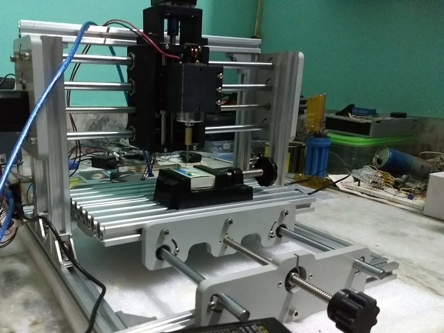


Our prototype model is IoT-based thus providing it a scalable architecture to use it from practically anywhere with an internetconnection. This is a 350mm x 350mm CNC with a 250mm x 240mm work area, running on open source motion control software (GRBL). Even our hardware is also mostly open source and thus comes the major cost cutting. This machine is made wholly from locally purchased items and can machine on wood, plastics, hard rubber, hard resin, etc. Our primary target is low-cost PCB manufacturing.
The prospect of wood craving is also there.
We’re planning to add laser machining support too as part of our future project.
As the system can bepresently controlled from a local Intranet wirelessly, we want to scale itf urther to make a distributed model web application to make and connect anecosystem of multiple number of these kind of devices.
The possibilities are unlimited with our machine.
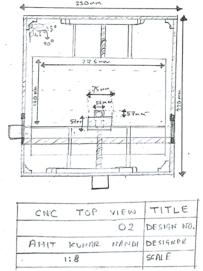
Our prototype model has its base frame made out of 2020 T-slotted aluminum extrusions and L-joints. The machine gives roughly about 80-85 Watts power with its 2000 rpm DC-controlled spindle. It has lead screw and threaded rod movement scheme with guiding smooth rods having radial groove snap fit ball bearings for smooth operations along all the 3 axes.
The minimum lead pitch is 0.8mm/revolution with a2000 steps/revolution we have a resolution of 1600 for all the axes. Our rough machine size is about 430x430x330mm and work area is about 270x170x65mm with 0.04mm positional accuracy. Our Z-axis gantry is 3D-printed from scratch with dual guiding rods.
The Z-axis travel 4.8 cm with spindle bit mounted. We’re using 45° V-bit cutting tool for PCB engraving purposes, it also supports 0.2mm to 1.8mm end mill bits. We’re using NEMA 23 Stepper motors with 3A maxcurrent for each axes main drive. The motors are driven by 2.5A A4988 drivers with 1/16th maximum micro-stepping resolution providing us theultimate machining precision at a very economic cost.
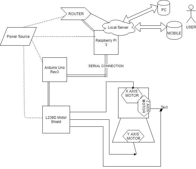
For the IoT part, we have made it possible to control the CNC router from a headless display like a mobile /tablet screen(acting as our HMI here) from anywhere with an Interne tconnection. We’re using a Raspberry Pi and a router (security) arrangement connected to the internet and running a web server to provide an interface for controlling our CNC wirelessly. We’re also planning to get hold of valuable machine part insights like real-time motor torque, current drawn, vibration, noise etc. and draw real time insights in a web platform for better collaboration. Which is perhaps called in the manufacturing sector as the Industrial IoT (INDUSTRY 4.0).

(Scribbled version of C:\Users\ABDERR~1\AppData\Local\Temp\ink_ext_XXXXXX.svgISF45X @ 3000.00)
( unicorn.py --tab="plotter_setup" --pen-up-angle=50 --pen-down-angle=30 --start-delay=160 --stop-delay=150 --xy-feedrate=3000 --z-feedrate=150 --z-height=0 --finished-height=0 --register-pen=true --x-home=0 --y-home=0 --num-copies=1 --continuous=false --pause-on-layer-change=true C:\Users\ABDERR~1\AppData\Local\Temp\ink_ext_XXXXXX.svgISF45X )
G21 (metric ftw)
G90 (absolute mode)
G92 X0.00 Y0.00 Z0.00 (you are here)

M300 S30 (pen down)
G4 P160 (wait 160ms)
M300 S50 (pen up)
G4 P150 (wait 150ms)
M18 (disengage drives)
M01 (Was registration test successful?)
M17 (engage drives if YES, and continue)

M01 (Plotting layer 'Calque 1')
(Polyline consisting of 29 segments.)
G1 X16.85 Y4.97 F3000.00
M300 S30.00 (pen down)
G4 P160 (wait 160ms)
G1 X14.07 Y5.98 F3000.00
G1 X13.33 Y6.40 F3000.00
G1 X10.74 Y6.40 F3000.00
G1 X8.14 Y6.49 F3000.00
G1 X10.60 Y6.58 F3000.00
G1 X13.07 Y6.64 F3000.00
G1 X12.75 Y6.98 F3000.00
G1 X11.99 Y8.33 F3000.00
G1 X12.30 Y9.13 F3000.00
G1 X12.98 Y9.85 F3000.00
G1 X14.73 Y10.48 F3000.00
G1 X16.42 Y10.34 F3000.00
G1 X16.89 Y10.16 F3000.00
G1 X17.20 Y10.44 F3000.00
G1 X17.44 Y10.92 F3000.00
G1 X15.95 Y12.12 F3000.00
G1 X14.52 Y13.21 F3000.00
G1 X14.17 Y14.50 F3000.00
G1 X14.18 Y14.85 F3000.00
G1 X13.90 Y14.95 F3000.00
G1 X13.30 Y15.34 F3000.00
G1 X13.02 Y16.08 F3000.00
G1 X13.23 Y16.62 F3000.00
G1 X14.03 Y16.94 F3000.00
G1 X14.80 Y16.89 F3000.00
G1 X15.21 Y16.80 F3000.00
G1 X15.35 Y17.02 F3000.00
G1 X15.71 Y17.77 F3000.00
G1 X16.05 Y18.61 F3000.00
G1 X15.77 Y19.35 F3000.00
G1 X15.47 Y20.24 F3000.00
G1 X15.20 Y20.73 F3000.00
G1 X13.98 Y20.91 F3000.00
G1 X12.47 Y21.26 F3000.00
G1 X11.32 Y21.88 F3000.00
G1 X10.23 Y23.00 F3000.00
G1 X9.82 Y24.17 F3000.00
G1 X9.94 Y24.90 F3000.00
G1 X10.41 Y25.47 F3000.00
G1 X10.77 Y25.78 F3000.00
G1 X10.53 Y26.37 F3000.00
G1 X10.04 Y28.07 F3000.00
G1 X10.02 Y29.68 F3000.00
G1 X10.50 Y31.25 F3000.00
G1 X11.46 Y32.80 F3000.00
G1 X13.34 Y34.54 F3000.00
G1 X15.75 Y36.02 F3000.00
G1 X16.94 Y36.57 F3000.00
G1 X11.31 Y36.60 F3000.00
G1 X5.53 Y36.58 F3000.00
G1 X5.38 Y21.60 F3000.00
G1 X5.41 Y8.55 F3000.00
G1 X5.62 Y6.61 F3000.00
G1 X5.85 Y6.48 F3000.00
G1 X5.50 Y6.40 F3000.00
G1 X5.14 Y6.40 F3000.00
G1 X5.14 Y21.60 F3000.00
G1 X5.14 Y36.80 F3000.00
G1 X11.39 Y36.80 F3000.00
G1 X17.65 Y36.80 F3000.00
G1 X18.65 Y37.07 F3000.00
G1 X21.13 Y37.54 F3000.00
G1 X23.70 Y37.69 F3000.00
G1 X26.12 Y37.52 F3000.00
G1 X28.11 Y37.03 F3000.00
G1 X28.70 Y36.80 F3000.00
G1 X33.01 Y36.80 F3000.00
G1 X37.32 Y36.80 F3000.00
G1 X37.32 Y21.60 F3000.00
G1 X37.32 Y6.40 F3000.00
G1 X32.21 Y6.40 F3000.00
G1 X26.73 Y6.25 F3000.00
G1 X22.57 Y5.07 F3000.00
G1 X16.85 Y4.97 F3000.00
G1 X16.85 Y4.97 F3000.00
M300 S50.00 (pen up)
G4 P150 (wait 150ms)

(Polyline consisting of 29 segments.)
G1 X20.57 Y5.03 F3000.00
M300 S30.00 (pen down)
G4 P160 (wait 160ms)
G1 X23.06 Y5.34 F3000.00
G1 X24.86 Y5.94 F3000.00
G1 X25.99 Y6.82 F3000.00
G1 X26.48 Y8.01 F3000.00
G1 X26.11 Y9.51 F3000.00
G1 X24.89 Y10.76 F3000.00
G1 X23.73 Y11.07 F3000.00
G1 X22.18 Y10.75 F3000.00
G1 X20.76 Y10.29 F3000.00
G1 X20.13 Y9.96 F3000.00
G1 X19.83 Y9.40 F3000.00
G1 X19.66 Y9.17 F3000.00
G1 X19.74 Y9.72 F3000.00
G1 X20.51 Y10.61 F3000.00
G1 X21.41 Y11.91 F3000.00
G1 X21.31 Y12.42 F3000.00
G1 X20.85 Y12.91 F3000.00
G1 X19.04 Y13.73 F3000.00
G1 X18.83 Y13.81 F3000.00
G1 X19.56 Y13.72 F3000.00
G1 X20.90 Y13.07 F3000.00
G1 X21.48 Y12.71 F3000.00
G1 X21.88 Y12.90 F3000.00
G1 X23.87 Y14.56 F3000.00
G1 X24.34 Y15.23 F3000.00
G1 X23.85 Y15.22 F3000.00
G1 X19.04 Y15.20 F3000.00
G1 X16.99 Y15.70 F3000.00
G1 X15.62 Y16.42 F3000.00
G1 X15.31 Y16.66 F3000.00
G1 X14.86 Y15.95 F3000.00
G1 X14.39 Y14.29 F3000.00
G1 X14.89 Y12.97 F3000.00
G1 X16.02 Y12.25 F3000.00
G1 X17.19 Y11.48 F3000.00
G1 X17.63 Y10.79 F3000.00
G1 X16.90 Y10.01 F3000.00
G1 X16.07 Y9.45 F3000.00
G1 X16.23 Y9.73 F3000.00
G1 X16.50 Y10.15 F3000.00
G1 X14.70 Y10.34 F3000.00
G1 X13.17 Y9.72 F3000.00
G1 X12.44 Y9.03 F3000.00
G1 X12.23 Y8.30 F3000.00
G1 X12.53 Y7.53 F3000.00
G1 X13.34 Y6.71 F3000.00
G1 X15.72 Y5.44 F3000.00
G1 X18.83 Y4.95 F3000.00
G1 X20.57 Y5.03 F3000.00
G1 X20.57 Y5.03 F3000.00
M300 S50.00 (pen up)
G4 P150 (wait 150ms)

(Polyline consisting of 29 segments.)
G1 X27.30 Y6.65 F3000.00
M300 S30.00 (pen down)
G4 P160 (wait 160ms)
G1 X29.25 Y7.52 F3000.00
G1 X30.16 Y8.34 F3000.00
G1 X30.46 Y9.06 F3000.00
G1 X30.29 Y9.88 F3000.00
G1 X29.49 Y10.84 F3000.00
G1 X28.16 Y11.51 F3000.00
G1 X26.25 Y11.62 F3000.00
G1 X25.07 Y10.96 F3000.00
G1 X25.51 Y10.50 F3000.00
G1 X26.26 Y9.62 F3000.00
G1 X26.58 Y8.19 F3000.00
G1 X26.44 Y7.12 F3000.00
G1 X25.77 Y6.34 F3000.00
G1 X25.47 Y6.07 F3000.00
G1 X25.68 Y6.08 F3000.00
G1 X27.30 Y6.65 F3000.00
G1 X27.30 Y6.65 F3000.00
M300 S50.00 (pen up)
G4 P150 (wait 150ms)

(Polyline consisting of 29 segments.)
G1 X37.06 Y21.42 F3000.00
M300 S30.00 (pen down)
G4 P160 (wait 160ms)
G1 X37.02 Y36.41 F3000.00
G1 X36.96 Y36.62 F3000.00
G1 X33.06 Y36.62 F3000.00
G1 X29.16 Y36.58 F3000.00
G1 X29.47 Y36.10 F3000.00
G1 X29.73 Y35.05 F3000.00
G1 X29.34 Y34.00 F3000.00
G1 X28.36 Y33.19 F3000.00
G1 X26.78 Y32.58 F3000.00
G1 X24.56 Y32.18 F3000.00
G1 X24.11 Y32.04 F3000.00
G1 X24.44 Y31.73 F3000.00
G1 X25.27 Y31.55 F3000.00
G1 X28.11 Y31.00 F3000.00
G1 X28.91 Y30.55 F3000.00
G1 X29.29 Y29.72 F3000.00
G1 X29.84 Y28.76 F3000.00
G1 X30.44 Y28.08 F3000.00
G1 X30.69 Y27.27 F3000.00
G1 X30.58 Y26.46 F3000.00
G1 X30.11 Y25.77 F3000.00
G1 X29.82 Y25.45 F3000.00
G1 X29.90 Y25.05 F3000.00
G1 X29.83 Y24.22 F3000.00
G1 X28.51 Y23.12 F3000.00
G1 X26.38 Y22.66 F3000.00
G1 X25.09 Y22.48 F3000.00
G1 X24.68 Y22.25 F3000.00
G1 X24.95 Y22.15 F3000.00
G1 X26.03 Y21.82 F3000.00
G1 X27.25 Y21.07 F3000.00
G1 X27.59 Y20.36 F3000.00
G1 X27.42 Y19.68 F3000.00
G1 X26.21 Y18.82 F3000.00
G1 X24.70 Y18.51 F3000.00
G1 X24.39 Y18.50 F3000.00
G1 X24.42 Y18.22 F3000.00
G1 X24.59 Y16.70 F3000.00
G1 X24.63 Y15.61 F3000.00
G1 X24.39 Y15.01 F3000.00
G1 X23.81 Y14.22 F3000.00
G1 X23.52 Y13.85 F3000.00
G1 X24.03 Y13.49 F3000.00
G1 X24.69 Y12.99 F3000.00
G1 X24.78 Y12.31 F3000.00
G1 X24.54 Y11.48 F3000.00
G1 X24.58 Y11.08 F3000.00
G1 X25.21 Y11.31 F3000.00
G1 X26.08 Y11.74 F3000.00
G1 X27.14 Y11.85 F3000.00
G1 X28.29 Y11.66 F3000.00
G1 X29.41 Y11.16 F3000.00
G1 X30.24 Y10.39 F3000.00
G1 X30.57 Y9.37 F3000.00
G1 X30.36 Y8.29 F3000.00
G1 X29.62 Y7.56 F3000.00
G1 X28.50 Y6.94 F3000.00
G1 X27.96 Y6.65 F3000.00
G1 X32.49 Y6.61 F3000.00
G1 X37.02 Y6.63 F3000.00
G1 X37.06 Y21.42 F3000.00
G1 X37.06 Y21.42 F3000.00
M300 S50.00 (pen up)
G4 P150 (wait 150ms)

(Polyline consisting of 29 segments.)
G1 X21.74 Y10.75 F3000.00
M300 S30.00 (pen down)
G4 P160 (wait 160ms)
G1 X23.52 Y11.21 F3000.00
G1 X24.24 Y11.32 F3000.00
G1 X24.56 Y12.13 F3000.00
G1 X24.48 Y12.99 F3000.00
G1 X23.87 Y13.45 F3000.00
G1 X23.38 Y13.75 F3000.00
G1 X22.69 Y13.25 F3000.00
G1 X21.76 Y12.68 F3000.00
G1 X21.57 Y12.14 F3000.00
G1 X21.44 Y11.41 F3000.00
G1 X20.80 Y10.64 F3000.00
G1 X20.54 Y10.34 F3000.00
G1 X21.74 Y10.75 F3000.00
G1 X21.74 Y10.75 F3000.00
M300 S50.00 (pen up)
G4 P150 (wait 150ms)

(Polyline consisting of 29 segments.)
G1 X14.28 Y15.20 F3000.00
M300 S30.00 (pen down)
G4 P160 (wait 160ms)
G1 X14.69 Y15.95 F3000.00
G1 X14.87 Y16.70 F3000.00
G1 X13.98 Y16.78 F3000.00
G1 X13.23 Y16.33 F3000.00
G1 X13.26 Y15.80 F3000.00
G1 X13.54 Y15.32 F3000.00
G1 X13.94 Y15.06 F3000.00
G1 X14.28 Y15.20 F3000.00
G1 X14.28 Y15.20 F3000.00
M300 S50.00 (pen up)
G4 P150 (wait 150ms)

(Polyline consisting of 29 segments.)
G1 X23.89 Y15.40 F3000.00
M300 S30.00 (pen down)
G4 P160 (wait 160ms)
G1 X24.27 Y15.61 F3000.00
G1 X24.44 Y16.05 F3000.00
G1 X24.22 Y18.19 F3000.00
G1 X24.03 Y18.95 F3000.00
G1 X23.02 Y18.27 F3000.00
G1 X20.70 Y17.13 F3000.00
G1 X19.62 Y17.10 F3000.00
G1 X18.46 Y17.41 F3000.00
G1 X16.91 Y18.21 F3000.00
G1 X16.22 Y18.67 F3000.00
G1 X16.19 Y18.46 F3000.00
G1 X15.83 Y17.68 F3000.00
G1 X15.47 Y16.93 F3000.00
G1 X16.23 Y16.20 F3000.00
G1 X18.05 Y15.51 F3000.00
G1 X21.11 Y15.23 F3000.00
G1 X23.89 Y15.40 F3000.00
M300 S50.00 (pen up)
G4 P150 (wait 150ms)

(Polyline consisting of 29 segments.)
G1 X21.29 Y17.47 F3000.00
M300 S30.00 (pen down)
G4 P160 (wait 160ms)
G1 X23.50 Y18.80 F3000.00
G1 X25.56 Y20.02 F3000.00
G1 X26.14 Y20.17 F3000.00
G1 X25.92 Y20.50 F3000.00
G1 X24.80 Y21.28 F3000.00
G1 X23.98 Y21.40 F3000.00
G1 X22.98 Y21.10 F3000.00
G1 X21.95 Y20.78 F3000.00
G1 X21.63 Y20.62 F3000.00
G1 X21.08 Y19.88 F3000.00
G1 X20.05 Y19.10 F3000.00
G1 X19.03 Y19.22 F3000.00
G1 X18.43 Y19.27 F3000.00
G1 X17.95 Y19.18 F3000.00
G1 X17.51 Y19.96 F3000.00
G1 X17.19 Y20.04 F3000.00
G1 X16.57 Y20.11 F3000.00
G1 X16.13 Y20.58 F3000.00
G1 X15.93 Y20.86 F3000.00
G1 X15.70 Y20.63 F3000.00
G1 X15.78 Y19.60 F3000.00
G1 X16.86 Y18.45 F3000.00
G1 X19.13 Y17.31 F3000.00
G1 X20.21 Y17.23 F3000.00
G1 X21.29 Y17.47 F3000.00
G1 X21.29 Y17.47 F3000.00
M300 S50.00 (pen up)
G4 P150 (wait 150ms)

(Polyline consisting of 29 segments.)
G1 X26.41 Y19.09 F3000.00
M300 S30.00 (pen down)
G4 P160 (wait 160ms)
G1 X27.14 Y19.61 F3000.00
G1 X27.43 Y20.17 F3000.00
G1 X27.29 Y20.74 F3000.00
G1 X26.71 Y21.31 F3000.00
G1 X25.56 Y21.85 F3000.00
G1 X24.35 Y22.08 F3000.00
G1 X21.62 Y21.55 F3000.00
G1 X21.69 Y21.22 F3000.00
G1 X21.91 Y20.88 F3000.00
G1 X22.79 Y21.19 F3000.00
G1 X24.30 Y21.49 F3000.00
G1 X25.22 Y21.29 F3000.00
G1 X25.94 Y20.72 F3000.00
G1 X26.24 Y20.20 F3000.00
G1 X25.65 Y19.87 F3000.00
G1 X24.63 Y19.41 F3000.00
G1 X24.25 Y18.98 F3000.00
G1 X24.58 Y18.70 F3000.00
G1 X25.38 Y18.71 F3000.00
G1 X26.41 Y19.09 F3000.00
M300 S50.00 (pen up)
G4 P150 (wait 150ms)

(Polyline consisting of 29 segments.)
G1 X20.47 Y19.52 F3000.00
M300 S30.00 (pen down)
G4 P160 (wait 160ms)
G1 X21.59 Y21.02 F3000.00
G1 X21.45 Y21.31 F3000.00
G1 X20.18 Y21.30 F3000.00
G1 X18.93 Y20.60 F3000.00
G1 X18.73 Y19.89 F3000.00
G1 X19.06 Y19.38 F3000.00
G1 X19.71 Y19.20 F3000.00
G1 X20.47 Y19.52 F3000.00
G1 X20.47 Y19.52 F3000.00
M300 S50.00 (pen up)
G4 P150 (wait 150ms)

(Polyline consisting of 29 segments.)
G1 X18.40 Y19.46 F3000.00
M300 S30.00 (pen down)
G4 P160 (wait 160ms)
G1 X18.59 Y20.01 F3000.00
G1 X18.80 Y20.68 F3000.00
G1 X19.52 Y21.20 F3000.00
G1 X19.94 Y21.43 F3000.00
G1 X19.77 Y21.57 F3000.00
G1 X19.01 Y21.70 F3000.00
G1 X18.36 Y21.46 F3000.00
G1 X17.92 Y20.91 F3000.00
G1 X17.75 Y20.12 F3000.00
G1 X18.11 Y19.31 F3000.00
G1 X18.40 Y19.46 F3000.00
M300 S50.00 (pen up)
G4 P150 (wait 150ms)

(Polyline consisting of 29 segments.)
G1 X17.34 Y20.21 F3000.00
M300 S30.00 (pen down)
G4 P160 (wait 160ms)
G1 X17.57 Y20.59 F3000.00
G1 X18.44 Y21.73 F3000.00
G1 X18.77 Y21.86 F3000.00
G1 X18.44 Y21.92 F3000.00
G1 X17.48 Y21.91 F3000.00
G1 X16.63 Y21.60 F3000.00
G1 X16.25 Y20.93 F3000.00
G1 X16.60 Y20.24 F3000.00
G1 X17.34 Y20.21 F3000.00
G1 X17.34 Y20.21 F3000.00
M300 S50.00 (pen up)
G4 P150 (wait 150ms)

(Polyline consisting of 29 segments.)
G1 X16.11 Y21.33 F3000.00
M300 S30.00 (pen down)
G4 P160 (wait 160ms)
G1 X17.34 Y22.06 F3000.00
G1 X18.96 Y21.93 F3000.00
G1 X19.98 Y21.60 F3000.00
G1 X22.66 Y21.94 F3000.00
G1 X25.66 Y22.90 F3000.00
G1 X27.77 Y24.32 F3000.00
G1 X28.39 Y24.96 F3000.00
G1 X27.58 Y24.90 F3000.00
G1 X25.33 Y24.89 F3000.00
G1 X26.59 Y25.01 F3000.00
G1 X28.53 Y25.22 F3000.00
G1 X29.82 Y25.72 F3000.00
G1 X30.47 Y26.50 F3000.00
G1 X30.47 Y27.56 F3000.00
G1 X29.78 Y28.65 F3000.00
G1 X28.52 Y29.02 F3000.00
G1 X27.29 Y28.75 F3000.00
G1 X26.23 Y27.86 F3000.00
G1 X25.65 Y27.41 F3000.00
G1 X24.92 Y27.29 F3000.00
G1 X24.65 Y27.31 F3000.00
G1 X24.86 Y27.34 F3000.00
G1 X25.18 Y27.38 F3000.00
G1 X24.95 Y27.67 F3000.00
G1 X24.54 Y28.37 F3000.00
G1 X23.69 Y29.39 F3000.00
G1 X23.07 Y30.03 F3000.00
G1 X23.26 Y29.99 F3000.00
G1 X24.15 Y29.94 F3000.00
G1 X24.73 Y30.08 F3000.00
G1 X24.88 Y30.40 F3000.00
G1 X25.06 Y30.76 F3000.00
G1 X25.72 Y30.30 F3000.00
G1 X26.44 Y29.84 F3000.00
G1 X27.29 Y29.51 F3000.00
G1 X28.61 Y29.15 F3000.00
G1 X29.24 Y29.13 F3000.00
G1 X29.14 Y29.58 F3000.00
G1 X28.98 Y30.21 F3000.00
G1 X27.91 Y30.88 F3000.00
G1 X25.68 Y31.34 F3000.00
G1 X22.80 Y31.52 F3000.00
G1 X19.80 Y31.37 F3000.00
G1 X18.50 Y31.23 F3000.00
G1 X18.49 Y31.31 F3000.00
G1 X22.58 Y31.67 F3000.00
G1 X24.11 Y31.73 F3000.00
G1 X23.99 Y31.95 F3000.00
G1 X23.36 Y32.13 F3000.00
G1 X20.76 Y32.50 F3000.00
G1 X20.31 Y32.72 F3000.00
G1 X21.00 Y32.57 F3000.00
G1 X23.09 Y32.33 F3000.00
G1 X25.50 Y32.44 F3000.00
G1 X27.74 Y33.07 F3000.00
G1 X29.12 Y34.03 F3000.00
G1 X29.56 Y35.31 F3000.00
G1 X28.81 Y36.44 F3000.00
G1 X27.64 Y37.03 F3000.00
G1 X25.83 Y37.40 F3000.00
G1 X21.36 Y37.42 F3000.00
G1 X17.13 Y36.41 F3000.00
G1 X13.56 Y34.53 F3000.00
G1 X12.16 Y33.30 F3000.00
G1 X11.08 Y31.92 F3000.00
G1 X10.41 Y30.48 F3000.00
G1 X10.25 Y28.79 F3000.00
G1 X10.59 Y26.73 F3000.00
G1 X10.96 Y25.92 F3000.00
G1 X11.64 Y26.09 F3000.00
G1 X14.41 Y26.25 F3000.00
G1 X14.93 Y26.37 F3000.00
G1 X18.16 Y28.80 F3000.00
G1 X19.16 Y29.37 F3000.00
G1 X19.89 Y29.55 F3000.00
G1 X21.95 Y29.85 F3000.00
G1 X21.69 Y29.97 F3000.00
G1 X21.49 Y30.07 F3000.00
G1 X22.66 Y29.69 F3000.00
G1 X23.99 Y28.19 F3000.00
G1 X22.32 Y28.67 F3000.00
G1 X19.99 Y29.36 F3000.00
G1 X19.26 Y29.28 F3000.00
G1 X18.96 Y28.62 F3000.00
G1 X18.86 Y28.24 F3000.00
G1 X18.84 Y28.58 F3000.00
G1 X18.72 Y28.93 F3000.00
G1 X16.87 Y27.79 F3000.00
G1 X15.17 Y26.36 F3000.00
G1 X15.64 Y25.80 F3000.00
G1 X16.13 Y25.37 F3000.00
G1 X15.74 Y25.56 F3000.00
G1 X14.85 Y25.99 F3000.00
G1 X13.66 Y26.16 F3000.00
G1 X11.44 Y25.87 F3000.00
G1 X10.64 Y25.45 F3000.00
G1 X10.13 Y24.87 F3000.00
G1 X10.03 Y23.93 F3000.00
G1 X10.90 Y22.46 F3000.00
G1 X12.38 Y21.47 F3000.00
G1 X15.35 Y20.88 F3000.00
G1 X16.11 Y21.33 F3000.00
G1 X16.11 Y21.33 F3000.00
M300 S50.00 (pen up)
G4 P150 (wait 150ms)

(Polyline consisting of 29 segments.)
G1 X20.69 Y22.24 F3000.00
M300 S30.00 (pen down)
G4 P160 (wait 160ms)
G1 X20.79 Y22.76 F3000.00
G1 X21.29 Y23.38 F3000.00
G1 X22.37 Y23.78 F3000.00
G1 X23.34 Y23.52 F3000.00
G1 X23.44 Y23.35 F3000.00
G1 X23.10 Y23.48 F3000.00
G1 X22.40 Y23.62 F3000.00
G1 X21.47 Y23.27 F3000.00
G1 X20.95 Y22.70 F3000.00
G1 X20.99 Y22.34 F3000.00
G1 X20.95 Y22.21 F3000.00
G1 X20.69 Y22.24 F3000.00
M300 S50.00 (pen up)
G4 P150 (wait 150ms)

(Polyline consisting of 29 segments.)
G1 X14.38 Y22.80 F3000.00
M300 S30.00 (pen down)
G4 P160 (wait 160ms)
G1 X13.38 Y23.55 F3000.00
G1 X13.10 Y23.93 F3000.00
G1 X13.67 Y24.07 F3000.00
G1 X14.55 Y23.88 F3000.00
G1 X14.63 Y23.70 F3000.00
G1 X14.39 Y23.52 F3000.00
G1 X14.16 Y23.28 F3000.00
G1 X14.51 Y22.88 F3000.00
G1 X15.06 Y22.64 F3000.00
G1 X15.20 Y22.59 F3000.00
G1 X14.92 Y22.47 F3000.00
G1 X14.38 Y22.80 F3000.00
G1 X14.38 Y22.80 F3000.00
M300 S50.00 (pen up)
G4 P150 (wait 150ms)

(Polyline consisting of 29 segments.)
G1 X12.06 Y23.03 F3000.00
M300 S30.00 (pen down)
G4 P160 (wait 160ms)
G1 X12.09 Y23.74 F3000.00
G1 X12.87 Y24.26 F3000.00
G1 X13.76 Y24.43 F3000.00
G1 X14.60 Y24.23 F3000.00
G1 X16.38 Y23.00 F3000.00
G1 X15.54 Y23.51 F3000.00
G1 X14.54 Y24.12 F3000.00
G1 X13.63 Y24.26 F3000.00
G1 X12.46 Y23.91 F3000.00
G1 X12.19 Y23.55 F3000.00
G1 X12.21 Y23.14 F3000.00
G1 X12.23 Y22.89 F3000.00
G1 X12.06 Y23.03 F3000.00
G1 X12.06 Y23.03 F3000.00
M300 S50.00 (pen up)
G4 P150 (wait 150ms)

(Polyline consisting of 29 segments.)
G1 X21.77 Y26.53 F3000.00
M300 S30.00 (pen down)
G4 P160 (wait 160ms)
G1 X20.93 Y27.02 F3000.00
G1 X20.39 Y27.69 F3000.00
G1 X20.47 Y29.03 F3000.00
G1 X20.47 Y28.66 F3000.00
G1 X20.46 Y27.93 F3000.00
G1 X20.81 Y27.32 F3000.00
G1 X20.97 Y27.19 F3000.00
G1 X20.93 Y27.34 F3000.00
G1 X21.01 Y27.75 F3000.00
G1 X21.46 Y27.92 F3000.00
G1 X21.99 Y27.74 F3000.00
G1 X22.19 Y27.29 F3000.00
G1 X21.82 Y26.88 F3000.00
G1 X21.45 Y26.76 F3000.00
G1 X21.85 Y26.63 F3000.00
G1 X22.79 Y26.50 F3000.00
G1 X23.47 Y26.76 F3000.00
G1 X23.76 Y27.26 F3000.00
G1 X23.87 Y27.64 F3000.00
G1 X23.99 Y27.52 F3000.00
G1 X23.83 Y26.97 F3000.00
G1 X23.03 Y26.40 F3000.00
G1 X21.77 Y26.53 F3000.00
G1 X21.77 Y26.53 F3000.00
M300 S50.00 (pen up)
G4 P150 (wait 150ms)

(Polyline consisting of 29 segments.)
G1 X27.79 Y22.99 F3000.00
M300 S30.00 (pen down)
G4 P160 (wait 160ms)
G1 X29.58 Y24.08 F3000.00
G1 X29.65 Y25.26 F3000.00
G1 X29.13 Y25.25 F3000.00
G1 X28.43 Y24.71 F3000.00
G1 X26.00 Y22.88 F3000.00
G1 X26.04 Y22.79 F3000.00
G1 X27.79 Y22.99 F3000.00
G1 X27.79 Y22.99 F3000.00
M300 S50.00 (pen up)
G4 P150 (wait 150ms)

(Polyline consisting of 29 segments.)
G1 X25.85 Y27.75 F3000.00
M300 S30.00 (pen down)
G4 P160 (wait 160ms)
G1 X26.10 Y28.24 F3000.00
G1 X25.81 Y28.87 F3000.00
G1 X24.91 Y29.47 F3000.00
G1 X24.81 Y29.07 F3000.00
G1 X25.01 Y28.67 F3000.00
G1 X25.41 Y28.54 F3000.00
G1 X25.55 Y28.20 F3000.00
G1 X25.36 Y27.82 F3000.00
G1 X25.25 Y27.58 F3000.00
G1 X25.43 Y27.46 F3000.00
G1 X25.85 Y27.75 F3000.00
M300 S50.00 (pen up)
G4 P150 (wait 150ms)

(Polyline consisting of 29 segments.)
G1 X23.53 Y28.63 F3000.00
M300 S30.00 (pen down)
G4 P160 (wait 160ms)
G1 X22.85 Y29.32 F3000.00
G1 X22.16 Y29.64 F3000.00
G1 X21.18 Y29.54 F3000.00
G1 X20.71 Y29.43 F3000.00
G1 X22.20 Y28.86 F3000.00
G1 X23.73 Y28.29 F3000.00
G1 X23.53 Y28.63 F3000.00
G1 X23.53 Y28.63 F3000.00
M300 S50.00 (pen up)
G4 P150 (wait 150ms)

(Polyline consisting of 29 segments.)
G1 X27.46 Y28.97 F3000.00
M300 S30.00 (pen down)
G4 P160 (wait 160ms)
G1 X27.72 Y29.09 F3000.00
G1 X26.09 Y29.77 F3000.00
G1 X25.56 Y29.96 F3000.00
G1 X25.77 Y29.98 F3000.00
G1 X25.59 Y30.22 F3000.00
G1 X25.15 Y30.48 F3000.00
G1 X25.02 Y30.03 F3000.00
G1 X25.02 Y29.65 F3000.00
G1 X25.34 Y29.43 F3000.00
G1 X26.04 Y28.78 F3000.00
G1 X26.34 Y28.31 F3000.00
G1 X26.77 Y28.61 F3000.00
G1 X27.46 Y28.97 F3000.00
G1 X27.46 Y28.97 F3000.00
M300 S50.00 (pen up)
G4 P150 (wait 150ms)

(Polyline consisting of 29 segments.)
G1 X24.71 Y29.72 F3000.00
M300 S30.00 (pen down)
G4 P160 (wait 160ms)
G1 X24.20 Y29.82 F3000.00
G1 X23.65 Y29.70 F3000.00
G1 X24.07 Y29.24 F3000.00
G1 X24.53 Y28.81 F3000.00
G1 X24.62 Y29.16 F3000.00
G1 X24.71 Y29.72 F3000.00
G1 X24.71 Y29.72 F3000.00
M300 S50.00 (pen up)
G4 P150 (wait 150ms)

(Polyline consisting of 29 segments.)
G1 X5.54 Y5.46 F3000.00
M300 S30.00 (pen down)
G4 P160 (wait 160ms)
G1 X5.91 Y5.48 F3000.00
G1 X5.65 Y5.39 F3000.00
G1 X5.54 Y5.46 F3000.00
G1 X5.54 Y5.46 F3000.00
M300 S50.00 (pen up)
G4 P150 (wait 150ms)

(Polyline consisting of 29 segments.)
G1 X6.11 Y5.52 F3000.00
M300 S30.00 (pen down)
G4 P160 (wait 160ms)
G1 X6.17 Y5.64 F3000.00
G1 X6.18 Y5.47 F3000.00
G1 X6.11 Y5.52 F3000.00
G1 X6.11 Y5.52 F3000.00
M300 S50.00 (pen up)
G4 P150 (wait 150ms)

(Polyline consisting of 29 segments.)
G1 X6.34 Y5.49 F3000.00
M300 S30.00 (pen down)
G4 P160 (wait 160ms)
G1 X6.88 Y5.56 F3000.00
G1 X7.42 Y5.50 F3000.00
G1 X6.88 Y5.43 F3000.00
G1 X6.34 Y5.49 F3000.00
M300 S50.00 (pen up)
G4 P150 (wait 150ms)

(Polyline consisting of 29 segments.)
G1 X7.58 Y5.52 F3000.00
M300 S30.00 (pen down)
G4 P160 (wait 160ms)
G1 X7.74 Y5.60 F3000.00
G1 X7.83 Y5.48 F3000.00
G1 X7.58 Y5.52 F3000.00
M300 S50.00 (pen up)
G4 P150 (wait 150ms)

(Polyline consisting of 29 segments.)
G1 X8.50 Y5.49 F3000.00
M300 S30.00 (pen down)
G4 P160 (wait 160ms)
G1 X8.86 Y5.58 F3000.00
G1 X9.21 Y5.51 F3000.00
G1 X8.86 Y5.42 F3000.00
G1 X8.50 Y5.49 F3000.00
M300 S50.00 (pen up)
G4 P150 (wait 150ms)

(Polyline consisting of 29 segments.)
G1 X6.75 Y6.41 F3000.00
M300 S30.00 (pen down)
G4 P160 (wait 160ms)
G1 X6.93 Y6.46 F3000.00
G1 X6.91 Y6.29 F3000.00
G1 X6.75 Y6.41 F3000.00
G1 X6.75 Y6.41 F3000.00
M300 S50.00 (pen up)
G4 P150 (wait 150ms)

(Polyline consisting of 29 segments.)
G1 X7.49 Y6.39 F3000.00
M300 S30.00 (pen down)
G4 P160 (wait 160ms)
G1 X7.53 Y6.53 F3000.00
G1 X7.70 Y6.45 F3000.00
G1 X7.49 Y6.39 F3000.00
G1 X7.49 Y6.39 F3000.00
M300 S50.00 (pen up)
G4 P150 (wait 150ms)

(Polyline consisting of 29 segments.)
G1 X16.85 Y4.97 F3000.00
M300 S30.00 (pen down)
G4 P160 (wait 160ms)
G1 X14.07 Y5.98 F3000.00
G1 X13.33 Y6.40 F3000.00
G1 X10.74 Y6.40 F3000.00
G1 X8.14 Y6.49 F3000.00
G1 X10.60 Y6.58 F3000.00
G1 X13.07 Y6.64 F3000.00
G1 X12.75 Y6.98 F3000.00
G1 X11.99 Y8.33 F3000.00
G1 X12.30 Y9.13 F3000.00
G1 X12.98 Y9.85 F3000.00
G1 X14.73 Y10.48 F3000.00
G1 X16.42 Y10.34 F3000.00
G1 X16.89 Y10.16 F3000.00
G1 X17.20 Y10.44 F3000.00
G1 X17.44 Y10.92 F3000.00
G1 X15.95 Y12.12 F3000.00
G1 X14.52 Y13.21 F3000.00
G1 X14.17 Y14.50 F3000.00
G1 X14.18 Y14.85 F3000.00
G1 X13.90 Y14.95 F3000.00
G1 X13.30 Y15.34 F3000.00
G1 X13.02 Y16.08 F3000.00
G1 X13.23 Y16.62 F3000.00
G1 X14.03 Y16.94 F3000.00
G1 X14.80 Y16.89 F3000.00
G1 X15.21 Y16.80 F3000.00
G1 X15.35 Y17.02 F3000.00
G1 X15.71 Y17.77 F3000.00
G1 X16.05 Y18.61 F3000.00
G1 X15.77 Y19.35 F3000.00
G1 X15.47 Y20.24 F3000.00
G1 X15.20 Y20.73 F3000.00
G1 X13.98 Y20.91 F3000.00
G1 X12.47 Y21.26 F3000.00
G1 X11.32 Y21.88 F3000.00
G1 X10.23 Y23.00 F3000.00
G1 X9.82 Y24.17 F3000.00
G1 X9.94 Y24.90 F3000.00
G1 X10.41 Y25.47 F3000.00
G1 X10.77 Y25.78 F3000.00
G1 X10.53 Y26.37 F3000.00
G1 X10.04 Y28.07 F3000.00
G1 X10.02 Y29.68 F3000.00
G1 X10.50 Y31.25 F3000.00
G1 X11.46 Y32.80 F3000.00
G1 X13.34 Y34.54 F3000.00
G1 X15.75 Y36.02 F3000.00
G1 X16.94 Y36.57 F3000.00
G1 X11.31 Y36.60 F3000.00
G1 X5.53 Y36.58 F3000.00
G1 X5.38 Y21.60 F3000.00
G1 X5.41 Y8.55 F3000.00
G1 X5.62 Y6.61 F3000.00
G1 X5.85 Y6.48 F3000.00
G1 X5.50 Y6.40 F3000.00
G1 X5.14 Y6.40 F3000.00
G1 X5.14 Y21.60 F3000.00
G1 X5.14 Y36.80 F3000.00
G1 X11.39 Y36.80 F3000.00
G1 X17.65 Y36.80 F3000.00
G1 X18.65 Y37.07 F3000.00
G1 X21.13 Y37.54 F3000.00
G1 X23.70 Y37.69 F3000.00
G1 X26.12 Y37.52 F3000.00
G1 X28.11 Y37.03 F3000.00
G1 X28.70 Y36.80 F3000.00
G1 X33.01 Y36.80 F3000.00
G1 X37.32 Y36.80 F3000.00
G1 X37.32 Y21.60 F3000.00
G1 X37.32 Y6.40 F3000.00
G1 X32.21 Y6.40 F3000.00
G1 X26.73 Y6.25 F3000.00
G1 X22.57 Y5.07 F3000.00
G1 X16.85 Y4.97 F3000.00
G1 X16.85 Y4.97 F3000.00
M300 S50.00 (pen up)
G4 P150 (wait 150ms)

(Polyline consisting of 29 segments.)
G1 X20.57 Y5.03 F3000.00
M300 S30.00 (pen down)
G4 P160 (wait 160ms)
G1 X23.06 Y5.34 F3000.00
G1 X24.86 Y5.94 F3000.00
G1 X25.99 Y6.82 F3000.00
G1 X26.48 Y8.01 F3000.00
G1 X26.11 Y9.51 F3000.00
G1 X24.89 Y10.76 F3000.00
G1 X23.73 Y11.07 F3000.00
G1 X22.18 Y10.75 F3000.00
G1 X20.76 Y10.29 F3000.00
G1 X20.13 Y9.96 F3000.00
G1 X19.83 Y9.40 F3000.00
G1 X19.66 Y9.17 F3000.00
G1 X19.74 Y9.72 F3000.00
G1 X20.51 Y10.61 F3000.00
G1 X21.41 Y11.91 F3000.00
G1 X21.31 Y12.42 F3000.00
G1 X20.85 Y12.91 F3000.00
G1 X19.04 Y13.73 F3000.00
G1 X18.83 Y13.81 F3000.00
G1 X19.56 Y13.72 F3000.00
G1 X20.90 Y13.07 F3000.00
G1 X21.48 Y12.71 F3000.00
G1 X21.88 Y12.90 F3000.00
G1 X23.87 Y14.56 F3000.00
G1 X24.34 Y15.23 F3000.00
G1 X23.85 Y15.22 F3000.00
G1 X19.04 Y15.20 F3000.00
G1 X16.99 Y15.70 F3000.00
G1 X15.62 Y16.42 F3000.00
G1 X15.31 Y16.66 F3000.00
G1 X14.86 Y15.95 F3000.00
G1 X14.39 Y14.29 F3000.00
G1 X14.89 Y12.97 F3000.00
G1 X16.02 Y12.25 F3000.00
G1 X17.19 Y11.48 F3000.00
G1 X17.63 Y10.79 F3000.00
G1 X16.90 Y10.01 F3000.00
G1 X16.07 Y9.45 F3000.00
G1 X16.23 Y9.73 F3000.00
G1 X16.50 Y10.15 F3000.00
G1 X14.70 Y10.34 F3000.00
G1 X13.17 Y9.72 F3000.00
G1 X12.44 Y9.03 F3000.00
G1 X12.23 Y8.30 F3000.00
G1 X12.53 Y7.53 F3000.00
G1 X13.34 Y6.71 F3000.00
G1 X15.72 Y5.44 F3000.00
G1 X18.83 Y4.95 F3000.00
G1 X20.57 Y5.03 F3000.00
G1 X20.57 Y5.03 F3000.00
M300 S50.00 (pen up)
G4 P150 (wait 150ms)

(Polyline consisting of 29 segments.)
G1 X27.30 Y6.65 F3000.00
M300 S30.00 (pen down)
G4 P160 (wait 160ms)
G1 X29.25 Y7.52 F3000.00
G1 X30.16 Y8.34 F3000.00
G1 X30.46 Y9.06 F3000.00
G1 X30.29 Y9.88 F3000.00
G1 X29.49 Y10.84 F3000.00
G1 X28.16 Y11.51 F3000.00
G1 X26.25 Y11.62 F3000.00
G1 X25.07 Y10.96 F3000.00
G1 X25.51 Y10.50 F3000.00
G1 X26.26 Y9.62 F3000.00
G1 X26.58 Y8.19 F3000.00
G1 X26.44 Y7.12 F3000.00
G1 X25.77 Y6.34 F3000.00
G1 X25.47 Y6.07 F3000.00
G1 X25.68 Y6.08 F3000.00
G1 X27.30 Y6.65 F3000.00
G1 X27.30 Y6.65 F3000.00
M300 S50.00 (pen up)
G4 P150 (wait 150ms)

(Polyline consisting of 29 segments.)
G1 X37.06 Y21.42 F3000.00
M300 S30.00 (pen down)
G4 P160 (wait 160ms)
G1 X37.02 Y36.41 F3000.00
G1 X36.96 Y36.62 F3000.00
G1 X33.06 Y36.62 F3000.00
G1 X29.16 Y36.58 F3000.00
G1 X29.47 Y36.10 F3000.00
G1 X29.73 Y35.05 F3000.00
G1 X29.34 Y34.00 F3000.00
G1 X28.36 Y33.19 F3000.00
G1 X26.78 Y32.58 F3000.00
G1 X24.56 Y32.18 F3000.00
G1 X24.11 Y32.04 F3000.00
G1 X24.44 Y31.73 F3000.00
G1 X25.27 Y31.55 F3000.00
G1 X28.11 Y31.00 F3000.00
G1 X28.91 Y30.55 F3000.00
G1 X29.29 Y29.72 F3000.00
G1 X29.84 Y28.76 F3000.00
G1 X30.44 Y28.08 F3000.00
G1 X30.69 Y27.27 F3000.00
G1 X30.58 Y26.46 F3000.00
G1 X30.11 Y25.77 F3000.00
G1 X29.82 Y25.45 F3000.00
G1 X29.90 Y25.05 F3000.00
G1 X29.83 Y24.22 F3000.00
G1 X28.51 Y23.12 F3000.00
G1 X26.38 Y22.66 F3000.00
G1 X25.09 Y22.48 F3000.00
G1 X24.68 Y22.25 F3000.00
G1 X24.95 Y22.15 F3000.00
G1 X26.03 Y21.82 F3000.00
G1 X27.25 Y21.07 F3000.00
G1 X27.59 Y20.36 F3000.00
G1 X27.42 Y19.68 F3000.00
G1 X26.21 Y18.82 F3000.00
G1 X24.70 Y18.51 F3000.00
G1 X24.39 Y18.50 F3000.00
G1 X24.42 Y18.22 F3000.00
G1 X24.59 Y16.70 F3000.00
G1 X24.63 Y15.61 F3000.00
G1 X24.39 Y15.01 F3000.00
G1 X23.81 Y14.22 F3000.00
G1 X23.52 Y13.85 F3000.00
G1 X24.03 Y13.49 F3000.00
G1 X24.69 Y12.99 F3000.00
G1 X24.78 Y12.31 F3000.00
G1 X24.54 Y11.48 F3000.00
G1 X24.58 Y11.08 F3000.00
G1 X25.21 Y11.31 F3000.00
G1 X26.08 Y11.74 F3000.00
G1 X27.14 Y11.85 F3000.00
G1 X28.29 Y11.66 F3000.00
G1 X29.41 Y11.16 F3000.00
G1 X30.24 Y10.39 F3000.00
G1 X30.57 Y9.37 F3000.00
...

This file has been truncated, please download it to see its full contents.
//AMIT
#include <Servo.h>
#include <AFMotor.h>

#define LINE_BUFFER_LENGTH 512

char STEP = MICROSTEP ;

// Servo position for Up and Down
const int penZUp = 115;
const int penZDown = 83;

// Servo on PWM pin 10
const int penServoPin =10 ;

// Should be right for DVD steppers, but is not too important here
const int stepsPerRevolution = 48;

// create servo object to control a servo
Servo penServo;

// Initialize steppers for X- and Y-axis using this Arduino pins for the L293D H-bridge
AF_Stepper myStepperY(stepsPerRevolution,1);
AF_Stepper myStepperX(stepsPerRevolution,2);

/* Structures, global variables    */
struct point {
  float x;
  float y;
  float z;
};

// Current position of plothead
struct point actuatorPos;

//  Drawing settings, should be OK
float StepInc = 1;
int StepDelay = 0;
int LineDelay =0;
int penDelay = 50;

// Motor steps to go 1 millimeter.
// Use test sketch to go 100 steps. Measure the length of line.
// Calculate steps per mm. Enter here.
float StepsPerMillimeterX = 100.0;
float StepsPerMillimeterY = 100.0;

// Drawing robot limits, in mm
// OK to start with. Could go up to 50 mm if calibrated well.
float Xmin = 0;
float Xmax = 40;
float Ymin = 0;
float Ymax = 40;
float Zmin = 0;
float Zmax = 1;

float Xpos = Xmin;
float Ypos = Ymin;
float Zpos = Zmax;

// Set to true to get debug output.
boolean verbose = false;

//  Needs to interpret
//  G1 for moving
//  G4 P300 (wait 150ms)
//  M300 S30 (pen down)
//  M300 S50 (pen up)
//  Discard anything with a (
//  Discard any other command!

/**********************
 * void setup() - Initialisations
 ***********************/
void setup() {
  //  Setup

  Serial.begin( 9600 );

  penServo.attach(penServoPin);
  penServo.write(penZUp);
  delay(100);

  // Decrease if necessary
  myStepperX.setSpeed(600);

  myStepperY.setSpeed(600);


  //  Set & move to initial default position
  // TBD

  //  Notifications!!!
  Serial.println("Mini CNC Plotter alive and kicking!");
  Serial.print("X range is from ");
  Serial.print(Xmin);
  Serial.print(" to ");
  Serial.print(Xmax);
  Serial.println(" mm.");
  Serial.print("Y range is from ");
  Serial.print(Ymin);
  Serial.print(" to ");
  Serial.print(Ymax);
  Serial.println(" mm.");
}

/**********************
 * void loop() - Main loop
 ***********************/
void loop()
{

  delay(100);
  char line[ LINE_BUFFER_LENGTH ];
  char c;
  int lineIndex;
  bool lineIsComment, lineSemiColon;

  lineIndex = 0;
  lineSemiColon = false;
  lineIsComment = false;

  while (1) {

    // Serial reception - Mostly from Grbl, added semicolon support
    while ( Serial.available()>0 ) {
      c = Serial.read();
      if (( c == '\n') || (c == '\r') ) {             // End of line reached
        if ( lineIndex > 0 ) {                        // Line is complete. Then execute!
          line[ lineIndex ] = '\0';                   // Terminate string
          if (verbose) {
            Serial.print( "Received : ");
            Serial.println( line );
          }
          processIncomingLine( line, lineIndex );
          lineIndex = 0;
        }
        else {
          // Empty or comment line. Skip block.
        }
        lineIsComment = false;
        lineSemiColon = false;
        Serial.println("ok");
      }
      else {
        if ( (lineIsComment) || (lineSemiColon) ) {   // Throw away all comment characters
          if ( c == ')' )  lineIsComment = false;     // End of comment. Resume line.
        }
        else {
          if ( c <= ' ' ) {                           // Throw away whitepace and control characters
          }
          else if ( c == '/' ) {                    // Block delete not supported. Ignore character.
          }
          else if ( c == '(' ) {                    // Enable comments flag and ignore all characters until ')' or EOL.
            lineIsComment = true;
          }
          else if ( c == ';' ) {
            lineSemiColon = true;
          }
          else if ( lineIndex >= LINE_BUFFER_LENGTH-1 ) {
            Serial.println( "ERROR - lineBuffer overflow" );
            lineIsComment = false;
            lineSemiColon = false;
          }
          else if ( c >= 'a' && c <= 'z' ) {        // Upcase lowercase
            line[ lineIndex++ ] = c-'a'+'A';
          }
          else {
            line[ lineIndex++ ] = c;
          }
        }
      }
    }
  }
}

void processIncomingLine( char* line, int charNB ) {
  int currentIndex = 0;
  char buffer[ 64 ];                                 // Hope that 64 is enough for 1 parameter
  struct point newPos;

  newPos.x = 0.0;
  newPos.y = 0.0;

  //  Needs to interpret
  //  G1 for moving
  //  G4 P300 (wait 150ms)
  //  G1 X60 Y30
  //  G1 X30 Y50
  //  M300 S30 (pen down)
  //  M300 S50 (pen up)
  //  Discard anything with a (
  //  Discard any other command!

  while( currentIndex < charNB ) {
    switch ( line[ currentIndex++ ] ) {              // Select command, if any
    case 'U':
      penUp();
      break;
    case 'D':
      penDown();
      break;
    case 'G':
      buffer[0] = line[ currentIndex++ ];          // /!\ Dirty - Only works with 2 digit commands
      //      buffer[1] = line[ currentIndex++ ];
      //      buffer[2] = '\0';
      buffer[1] = '\0';

      switch ( atoi( buffer ) ){                   // Select G command
      case 0:                                   // G00 & G01 - Movement or fast movement. Same here
      case 1:
        // /!\ Dirty - Suppose that X is before Y
        char* indexX = strchr( line+currentIndex, 'X' );  // Get X/Y position in the string (if any)
        char* indexY = strchr( line+currentIndex, 'Y' );
        if ( indexY <= 0 ) {
          newPos.x = atof( indexX + 1);
          newPos.y = actuatorPos.y;
        }
        else if ( indexX <= 0 ) {
          newPos.y = atof( indexY + 1);
          newPos.x = actuatorPos.x;
        }
        else {
          newPos.y = atof( indexY + 1);
          indexY = '\0';
          newPos.x = atof( indexX + 1);
        }
        drawLine(newPos.x, newPos.y );
        //        Serial.println("ok");
        actuatorPos.x = newPos.x;
        actuatorPos.y = newPos.y;
        break;
      }
      break;
    case 'M':
      buffer[0] = line[ currentIndex++ ];        // /!\ Dirty - Only works with 3 digit commands
      buffer[1] = line[ currentIndex++ ];
      buffer[2] = line[ currentIndex++ ];
      buffer[3] = '\0';
      switch ( atoi( buffer ) ){
      case 300:
        {
          char* indexS = strchr( line+currentIndex, 'S' );
          float Spos = atof( indexS + 1);
          //         Serial.println("ok");
          if (Spos == 30) {
            penDown();
          }
          if (Spos == 50) {
            penUp();
          }
          break;
        }
      case 114:                                // M114 - Repport position
        Serial.print( "Absolute position : X = " );
        Serial.print( actuatorPos.x );
        Serial.print( "  -  Y = " );
        Serial.println( actuatorPos.y );
        break;
      default:
        Serial.print( "Command not recognized : M");
        Serial.println( buffer );
      }
    }
  }


}


/*********************************
 * Draw a line from (x0;y0) to (x1;y1).
 * int (x1;y1) : Starting coordinates
 * int (x2;y2) : Ending coordinates
 **********************************/
void drawLine(float x1, float y1) {

  if (verbose)
  {
    Serial.print("fx1, fy1: ");
    Serial.print(x1);
    Serial.print(",");
    Serial.print(y1);
    Serial.println("");
  }

  //  Bring instructions within limits
  if (x1 >= Xmax) {
    x1 = Xmax;
  }
  if (x1 <= Xmin) {
    x1 = Xmin;
  }
  if (y1 >= Ymax) {
    y1 = Ymax;
  }
  if (y1 <= Ymin) {
    y1 = Ymin;
  }

  if (verbose)
  {
    Serial.print("Xpos, Ypos: ");
    Serial.print(Xpos);
    Serial.print(",");
    Serial.print(Ypos);
    Serial.println("");
  }

  if (verbose)
  {
    Serial.print("x1, y1: ");
    Serial.print(x1);
    Serial.print(",");
    Serial.print(y1);
    Serial.println("");
  }

  //  Convert coordinates to steps
  x1 = (int)(x1*StepsPerMillimeterX);
  y1 = (int)(y1*StepsPerMillimeterY);
  float x0 = Xpos;
  float y0 = Ypos;

  //  Let's find out the change for the coordinates
  long dx = abs(x1-x0);
  long dy = abs(y1-y0);
  int sx = x0<x1 ? StepInc : -StepInc;
  int sy = y0<y1 ? StepInc : -StepInc;

  long i;
  long over = 0;

  if (dx > dy) {
    for (i=0; i<dx; ++i) {
      myStepperX.onestep(sx,STEP);
      over+=dy;
      if (over>=dx) {
        over-=dx;
        myStepperY.onestep(sy,STEP);
      }
    delay(StepDelay);
    }
  }
  else {
    for (i=0; i<dy; ++i) {
      myStepperY.onestep(sy,STEP);
      over+=dx;
      if (over>=dy) {
        over-=dy;
        myStepperX.onestep(sx,STEP);
      }
      delay(StepDelay);
    }
  }

  if (verbose)
  {
    Serial.print("dx, dy:");
    Serial.print(dx);
    Serial.print(",");
    Serial.print(dy);
    Serial.println("");
  }

  if (verbose)
  {
    Serial.print("Going to (");
    Serial.print(x0);
    Serial.print(",");
    Serial.print(y0);
    Serial.println(")");
  }

  //  Delay before any next lines are submitted
  delay(LineDelay);
  //  Update the positions
  Xpos = x1;
  Ypos = y1;
}

//  Raises pen
void penUp() {
  penServo.write(penZUp);
  delay(penDelay);
  Zpos=Zmax;
  digitalWrite(15, LOW);
    digitalWrite(16, HIGH);
  if (verbose) {
    Serial.println("Pen up!");

  }
}
//  Lowers pen
void penDown() {
  penServo.write(penZDown);
  delay(penDelay);
  Zpos=Zmin;
  digitalWrite(15, HIGH);
    digitalWrite(16, LOW);
  if (verbose) {
    Serial.println("Pen down.");


  }
}
// Adafruit Motor shield library
// copyright Adafruit Industries LLC, 2009
// this code is public domain, enjoy!


#if (ARDUINO >= 100)
  #include "Arduino.h"
#else
  #if defined(__AVR__)
    #include <avr/io.h>
  #endif
  #include "WProgram.h"
#endif

#include "AFMotor.h"


static uint8_t latch_state;

#if (MICROSTEPS == 8)
uint8_t microstepcurve[] = {0, 50, 98, 142, 180, 212, 236, 250, 255};
#elif (MICROSTEPS == 16)
uint8_t microstepcurve[] = {0, 25, 50, 74, 98, 120, 141, 162, 180, 197, 212, 225, 236, 244, 250, 253, 255};
#endif

AFMotorController::AFMotorController(void) {
    TimerInitalized = false;
}

void AFMotorController::enable(void) {
  // setup the latch
  /*
  LATCH_DDR |= _BV(LATCH);
  ENABLE_DDR |= _BV(ENABLE);
  CLK_DDR |= _BV(CLK);
  SER_DDR |= _BV(SER);
  */
  pinMode(MOTORLATCH, OUTPUT);
  pinMode(MOTORENABLE, OUTPUT);
  pinMode(MOTORDATA, OUTPUT);
  pinMode(MOTORCLK, OUTPUT);

  latch_state = 0;

  latch_tx();  // "reset"

  //ENABLE_PORT &= ~_BV(ENABLE); // enable the chip outputs!
  digitalWrite(MOTORENABLE, LOW);
}


void AFMotorController::latch_tx(void) {
  uint8_t i;

  //LATCH_PORT &= ~_BV(LATCH);
  digitalWrite(MOTORLATCH, LOW);

  //SER_PORT &= ~_BV(SER);
  digitalWrite(MOTORDATA, LOW);

  for (i=0; i<8; i++) {
    //CLK_PORT &= ~_BV(CLK);
    digitalWrite(MOTORCLK, LOW);

    if (latch_state & _BV(7-i)) {
      //SER_PORT |= _BV(SER);
      digitalWrite(MOTORDATA, HIGH);
    } else {
      //SER_PORT &= ~_BV(SER);
      digitalWrite(MOTORDATA, LOW);
    }
    //CLK_PORT |= _BV(CLK);
    digitalWrite(MOTORCLK, HIGH);
  }
  //LATCH_PORT |= _BV(LATCH);
  digitalWrite(MOTORLATCH, HIGH);
}

static AFMotorController MC;

/******************************************
               MOTORS
******************************************/
inline void initPWM1(uint8_t freq) {
#if defined(__AVR_ATmega8__) || \
    defined(__AVR_ATmega48__) || \
    defined(__AVR_ATmega88__) || \
    defined(__AVR_ATmega168__) || \
    defined(__AVR_ATmega328P__)
    // use PWM from timer2A on PB3 (Arduino pin #11)
    TCCR2A |= _BV(COM2A1) | _BV(WGM20) | _BV(WGM21); // fast PWM, turn on oc2a
    TCCR2B = freq & 0x7;
    OCR2A = 0;
#elif defined(__AVR_ATmega1280__) || defined(__AVR_ATmega2560__)
    // on arduino mega, pin 11 is now PB5 (OC1A)
    TCCR1A |= _BV(COM1A1) | _BV(WGM10); // fast PWM, turn on oc1a
    TCCR1B = (freq & 0x7) | _BV(WGM12);
    OCR1A = 0;
#elif defined(__PIC32MX__)
    #if defined(PIC32_USE_PIN9_FOR_M1_PWM)
        // Make sure that pin 11 is an input, since we have tied together 9 and 11
        pinMode(9, OUTPUT);
        pinMode(11, INPUT);
        if (!MC.TimerInitalized)
        {   // Set up Timer2 for 80MHz counting fro 0 to 256
            T2CON = 0x8000 | ((freq & 0x07) << 4); // ON=1, FRZ=0, SIDL=0, TGATE=0, TCKPS=<freq>, T32=0, TCS=0; // ON=1, FRZ=0, SIDL=0, TGATE=0, TCKPS=0, T32=0, TCS=0
            TMR2 = 0x0000;
            PR2 = 0x0100;
            MC.TimerInitalized = true;
        }
         // Setup OC4 (pin 9) in PWM mode, with Timer2 as timebase
        OC4CON = 0x8006;    // OC32 = 0, OCTSEL=0, OCM=6
        OC4RS = 0x0000;
        OC4R = 0x0000;
    #elif defined(PIC32_USE_PIN10_FOR_M1_PWM)
        // Make sure that pin 11 is an input, since we have tied together 9 and 11
        pinMode(10, OUTPUT);
        pinMode(11, INPUT);
        if (!MC.TimerInitalized)
        {   // Set up Timer2 for 80MHz counting fro 0 to 256
            T2CON = 0x8000 | ((freq & 0x07) << 4); // ON=1, FRZ=0, SIDL=0, TGATE=0, TCKPS=<freq>, T32=0, TCS=0; // ON=1, FRZ=0, SIDL=0, TGATE=0, TCKPS=0, T32=0, TCS=0
            TMR2 = 0x0000;
            PR2 = 0x0100;
            MC.TimerInitalized = true;
        }
         // Setup OC5 (pin 10) in PWM mode, with Timer2 as timebase
        OC5CON = 0x8006;    // OC32 = 0, OCTSEL=0, OCM=6
        OC5RS = 0x0000;
        OC5R = 0x0000;
    #else
        // If we are not using PWM for pin 11, then just do digital
        digitalWrite(11, LOW);
    #endif
#else
   #error "This chip is not supported!"
#endif
    #if !defined(PIC32_USE_PIN9_FOR_M1_PWM) && !defined(PIC32_USE_PIN10_FOR_M1_PWM)
        pinMode(11, OUTPUT);
    #endif
}

inline void setPWM1(uint8_t s) {
#if defined(__AVR_ATmega8__) || \
    defined(__AVR_ATmega48__) || \
    defined(__AVR_ATmega88__) || \
    defined(__AVR_ATmega168__) || \
    defined(__AVR_ATmega328P__)
    // use PWM from timer2A on PB3 (Arduino pin #11)
    OCR2A = s;
#elif defined(__AVR_ATmega1280__) || defined(__AVR_ATmega2560__)
    // on arduino mega, pin 11 is now PB5 (OC1A)
    OCR1A = s;
#elif defined(__PIC32MX__)
    #if defined(PIC32_USE_PIN9_FOR_M1_PWM)
        // Set the OC4 (pin 9) PMW duty cycle from 0 to 255
        OC4RS = s;
    #elif defined(PIC32_USE_PIN10_FOR_M1_PWM)
        // Set the OC5 (pin 10) PMW duty cycle from 0 to 255
        OC5RS = s;
    #else
        // If we are not doing PWM output for M1, then just use on/off
        if (s > 127)
        {
            digitalWrite(11, HIGH);
        }
        else
        {
            digitalWrite(11, LOW);
        }
    #endif
#else
   #error "This chip is not supported!"
#endif
}

inline void initPWM2(uint8_t freq) {
#if defined(__AVR_ATmega8__) || \
    defined(__AVR_ATmega48__) || \
    defined(__AVR_ATmega88__) || \
    defined(__AVR_ATmega168__) || \
    defined(__AVR_ATmega328P__)
    // use PWM from timer2B (pin 3)
    TCCR2A |= _BV(COM2B1) | _BV(WGM20) | _BV(WGM21); // fast PWM, turn on oc2b
    TCCR2B = freq & 0x7;
    OCR2B = 0;
#elif defined(__AVR_ATmega1280__) || defined(__AVR_ATmega2560__)
    // on arduino mega, pin 3 is now PE5 (OC3C)
    TCCR3A |= _BV(COM1C1) | _BV(WGM10); // fast PWM, turn on oc3c
    TCCR3B = (freq & 0x7) | _BV(WGM12);
    OCR3C = 0;
#elif defined(__PIC32MX__)
    if (!MC.TimerInitalized)
    {   // Set up Timer2 for 80MHz counting fro 0 to 256
        T2CON = 0x8000 | ((freq & 0x07) << 4); // ON=1, FRZ=0, SIDL=0, TGATE=0, TCKPS=<freq>, T32=0, TCS=0; // ON=1, FRZ=0, SIDL=0, TGATE=0, TCKPS=0, T32=0, TCS=0
        TMR2 = 0x0000;
        PR2 = 0x0100;
        MC.TimerInitalized = true;
    }
    // Setup OC1 (pin3) in PWM mode, with Timer2 as timebase
    OC1CON = 0x8006;    // OC32 = 0, OCTSEL=0, OCM=6
    OC1RS = 0x0000;
    OC1R = 0x0000;
#else
   #error "This chip is not supported!"
#endif

    pinMode(3, OUTPUT);
}

inline void setPWM2(uint8_t s) {
#if defined(__AVR_ATmega8__) || \
    defined(__AVR_ATmega48__) || \
    defined(__AVR_ATmega88__) || \
    defined(__AVR_ATmega168__) || \
    defined(__AVR_ATmega328P__)
    // use PWM from timer2A on PB3 (Arduino pin #11)
    OCR2B = s;
#elif defined(__AVR_ATmega1280__) || defined(__AVR_ATmega2560__)
    // on arduino mega, pin 11 is now PB5 (OC1A)
    OCR3C = s;
#elif defined(__PIC32MX__)
    // Set the OC1 (pin3) PMW duty cycle from 0 to 255
    OC1RS = s;
#else
   #error "This chip is not supported!"
#endif
}

inline void initPWM3(uint8_t freq) {
#if defined(__AVR_ATmega8__) || \
    defined(__AVR_ATmega48__) || \
    defined(__AVR_ATmega88__) || \
    defined(__AVR_ATmega168__) || \
    defined(__AVR_ATmega328P__)
    // use PWM from timer0A / PD6 (pin 6)
    TCCR0A |= _BV(COM0A1) | _BV(WGM00) | _BV(WGM01); // fast PWM, turn on OC0A
    //TCCR0B = freq & 0x7;
    OCR0A = 0;
#elif defined(__AVR_ATmega1280__) || defined(__AVR_ATmega2560__)
    // on arduino mega, pin 6 is now PH3 (OC4A)
    TCCR4A |= _BV(COM1A1) | _BV(WGM10); // fast PWM, turn on oc4a
    TCCR4B = (freq & 0x7) | _BV(WGM12);
    //TCCR4B = 1 | _BV(WGM12);
    OCR4A = 0;
#elif defined(__PIC32MX__)
    if (!MC.TimerInitalized)
    {   // Set up Timer2 for 80MHz counting fro 0 to 256
        T2CON = 0x8000 | ((freq & 0x07) << 4); // ON=1, FRZ=0, SIDL=0, TGATE=0, TCKPS=<freq>, T32=0, TCS=0; // ON=1, FRZ=0, SIDL=0, TGATE=0, TCKPS=0, T32=0, TCS=0
        TMR2 = 0x0000;
        PR2 = 0x0100;
        MC.TimerInitalized = true;
    }
    // Setup OC3 (pin 6) in PWM mode, with Timer2 as timebase
    OC3CON = 0x8006;    // OC32 = 0, OCTSEL=0, OCM=6
    OC3RS = 0x0000;
    OC3R = 0x0000;
#else
   #error "This chip is not supported!"
#endif
    pinMode(6, OUTPUT);
}

inline void setPWM3(uint8_t s) {
#if defined(__AVR_ATmega8__) || \
    defined(__AVR_ATmega48__) || \
    defined(__AVR_ATmega88__) || \
    defined(__AVR_ATmega168__) || \
    defined(__AVR_ATmega328P__)
    // use PWM from timer0A on PB3 (Arduino pin #6)
    OCR0A = s;
#elif defined(__AVR_ATmega1280__) || defined(__AVR_ATmega2560__)
    // on arduino mega, pin 6 is now PH3 (OC4A)
    OCR4A = s;
#elif defined(__PIC32MX__)
    // Set the OC3 (pin 6) PMW duty cycle from 0 to 255
    OC3RS = s;
#else
   #error "This chip is not supported!"
#endif
}


inline void initPWM4(uint8_t freq) {
#if defined(__AVR_ATmega8__) || \
    defined(__AVR_ATmega48__) || \
    defined(__AVR_ATmega88__) || \
    defined(__AVR_ATmega168__) || \
    defined(__AVR_ATmega328P__)
    // use PWM from timer0B / PD5 (pin 5)
    TCCR0A |= _BV(COM0B1) | _BV(WGM00) | _BV(WGM01); // fast PWM, turn on oc0a
    //TCCR0B = freq & 0x7;
    OCR0B = 0;
#elif defined(__AVR_ATmega1280__) || defined(__AVR_ATmega2560__)
    // on arduino mega, pin 5 is now PE3 (OC3A)
    TCCR3A |= _BV(COM1A1) | _BV(WGM10); // fast PWM, turn on oc3a
    TCCR3B = (freq & 0x7) | _BV(WGM12);
    //TCCR4B = 1 | _BV(WGM12);
    OCR3A = 0;
#elif defined(__PIC32MX__)
    if (!MC.TimerInitalized)
    {   // Set up Timer2 for 80MHz counting fro 0 to 256
        T2CON = 0x8000 | ((freq & 0x07) << 4); // ON=1, FRZ=0, SIDL=0, TGATE=0, TCKPS=<freq>, T32=0, TCS=0; // ON=1, FRZ=0, SIDL=0, TGATE=0, TCKPS=0, T32=0, TCS=0
        TMR2 = 0x0000;
        PR2 = 0x0100;
        MC.TimerInitalized = true;
    }
    // Setup OC2 (pin 5) in PWM mode, with Timer2 as timebase
    OC2CON = 0x8006;    // OC32 = 0, OCTSEL=0, OCM=6
    OC2RS = 0x0000;
    OC2R = 0x0000;
#else
   #error "This chip is not supported!"
#endif
    pinMode(5, OUTPUT);
}

inline void setPWM4(uint8_t s) {
#if defined(__AVR_ATmega8__) || \
    defined(__AVR_ATmega48__) || \
    defined(__AVR_ATmega88__) || \
    defined(__AVR_ATmega168__) || \
    defined(__AVR_ATmega328P__)
    // use PWM from timer0A on PB3 (Arduino pin #6)
    OCR0B = s;
#elif defined(__AVR_ATmega1280__) || defined(__AVR_ATmega2560__)
    // on arduino mega, pin 6 is now PH3 (OC4A)
    OCR3A = s;
#elif defined(__PIC32MX__)
    // Set the OC2 (pin 5) PMW duty cycle from 0 to 255
    OC2RS = s;
#else
   #error "This chip is not supported!"
#endif
}

AF_DCMotor::AF_DCMotor(uint8_t num, uint8_t freq) {
  motornum = num;
  pwmfreq = freq;

  MC.enable();

  switch (num) {
  case 1:
    latch_state &= ~_BV(MOTOR1_A) & ~_BV(MOTOR1_B); // set both motor pins to 0
    MC.latch_tx();
    initPWM1(freq);
    break;
  case 2:
    latch_state &= ~_BV(MOTOR2_A) & ~_BV(MOTOR2_B); // set both motor pins to 0
    MC.latch_tx();
    initPWM2(freq);
    break;
  case 3:
    latch_state &= ~_BV(MOTOR3_A) & ~_BV(MOTOR3_B); // set both motor pins to 0
    MC.latch_tx();
    initPWM3(freq);
    break;
  case 4:
    latch_state &= ~_BV(MOTOR4_A) & ~_BV(MOTOR4_B); // set both motor pins to 0
    MC.latch_tx();
    initPWM4(freq);
    break;
  }
}

void AF_DCMotor::run(uint8_t cmd) {
  uint8_t a, b;
  switch (motornum) {
  case 1:
    a = MOTOR1_A; b = MOTOR1_B; break;
  case 2:
    a = MOTOR2_A; b = MOTOR2_B; break;
  case 3:
    a = MOTOR3_A; b = MOTOR3_B; break;
  case 4:
    a = MOTOR4_A; b = MOTOR4_B; break;
  default:
    return;
  }

  switch (cmd) {
  case FORWARD:
    latch_state |= _BV(a);
    latch_state &= ~_BV(b);
    MC.latch_tx();
    break;
  case BACKWARD:
    latch_state &= ~_BV(a);
    latch_state |= _BV(b);
    MC.latch_tx();
    break;
  case RELEASE:
    latch_state &= ~_BV(a);     // A and B both low
    latch_state &= ~_BV(b);
    MC.latch_tx();
    break;
  }
}

void AF_DCMotor::setSpeed(uint8_t speed) {
  switch (motornum) {
  case 1:
    setPWM1(speed); break;
  case 2:
    setPWM2(speed); break;
  case 3:
    setPWM3(speed); break;
  case 4:
    setPWM4(speed); break;
  }
}

/******************************************
               STEPPERS
******************************************/

AF_Stepper::AF_Stepper(uint16_t steps, uint8_t num) {
  MC.enable();

  revsteps = steps;
  steppernum = num;
  currentstep = 0;

  if (steppernum == 1) {
    latch_state &= ~_BV(MOTOR1_A) & ~_BV(MOTOR1_B) &
      ~_BV(MOTOR2_A) & ~_BV(MOTOR2_B); // all motor pins to 0
    MC.latch_tx();

    // enable both H bridges
    pinMode(11, OUTPUT);
    pinMode(3, OUTPUT);
    digitalWrite(11, HIGH);
    digitalWrite(3, HIGH);

    // use PWM for microstepping support
    initPWM1(STEPPER1_PWM_RATE);
    initPWM2(STEPPER1_PWM_RATE);
    setPWM1(255);
    setPWM2(255);

  } else if (steppernum == 2) {
    latch_state &= ~_BV(MOTOR3_A) & ~_BV(MOTOR3_B) &
      ~_BV(MOTOR4_A) & ~_BV(MOTOR4_B); // all motor pins to 0
    MC.latch_tx();

    // enable both H bridges
    pinMode(5, OUTPUT);
    pinMode(6, OUTPUT);
    digitalWrite(5, HIGH);
    digitalWrite(6, HIGH);

    // use PWM for microstepping support
    // use PWM for microstepping support
    initPWM3(STEPPER2_PWM_RATE);
    initPWM4(STEPPER2_PWM_RATE);
    setPWM3(255);
    setPWM4(255);
  }
}

void AF_Stepper::setSpeed(uint16_t rpm) {
  usperstep = 60000000 / ((uint32_t)revsteps * (uint32_t)rpm);
  steppingcounter = 0;
}

void AF_Stepper::release(void) {
  if (steppernum == 1) {
    latch_state &= ~_BV(MOTOR1_A) & ~_BV(MOTOR1_B) &
      ~_BV(MOTOR2_A) & ~_BV(MOTOR2_B); // all motor pins to 0
    MC.latch_tx();
  } else if (steppernum == 2) {
    latch_state &= ~_BV(MOTOR3_A) & ~_BV(MOTOR3_B) &
      ~_BV(MOTOR4_A) & ~_BV(MOTOR4_B); // all motor pins to 0
    MC.latch_tx();
  }
}

void AF_Stepper::step(uint16_t steps, uint8_t dir,  uint8_t style) {
  uint32_t uspers = usperstep;
  uint8_t ret = 0;

  if (style == INTERLEAVE) {
    uspers /= 2;
  }
 else if (style == MICROSTEP) {
    uspers /= MICROSTEPS;
    steps *= MICROSTEPS;
#ifdef MOTORDEBUG
    Serial.print("steps = "); Serial.println(steps, DEC);
#endif
  }

  while (steps--) {
    ret = onestep(dir, style);
    delay(uspers/1000); // in ms
    steppingcounter += (uspers % 1000);
    if (steppingcounter >= 1000) {
      delay(1);
      steppingcounter -= 1000;
    }
  }
  if (style == MICROSTEP) {
    while ((ret != 0) && (ret != MICROSTEPS)) {
      ret = onestep(dir, style);
      delay(uspers/1000); // in ms
      steppingcounter += (uspers % 1000);
      if (steppingcounter >= 1000) {
	delay(1);
	steppingcounter -= 1000;
      }
    }
  }
}

uint8_t AF_Stepper::onestep(uint8_t dir, uint8_t style) {
  uint8_t a, b, c, d;
  uint8_t ocrb, ocra;

  ocra = ocrb = 255;

  if (steppernum == 1) {
    a = _BV(MOTOR1_A);
    b = _BV(MOTOR2_A);
    c = _BV(MOTOR1_B);
    d = _BV(MOTOR2_B);
  } else if (steppernum == 2) {
    a = _BV(MOTOR3_A);
    b = _BV(MOTOR4_A);
    c = _BV(MOTOR3_B);
    d = _BV(MOTOR4_B);
  } else {
    return 0;
  }

  // next determine what sort of stepping procedure we're up to
  if (style == SINGLE) {
    if ((currentstep/(MICROSTEPS/2)) % 2) { // we're at an odd step, weird
      if (dir == FORWARD) {
	currentstep += MICROSTEPS/2;
      }
      else {
	currentstep -= MICROSTEPS/2;
      }
    } else {           // go to the next even step
      if (dir == FORWARD) {
	currentstep += MICROSTEPS;
      }
      else {
	currentstep -= MICROSTEPS;
      }
    }
  } else if (style == DOUBLE) {
    if (! (currentstep/(MICROSTEPS/2) % 2)) { // we're at an even step, weird
      if (dir == FORWARD) {
	currentstep += MICROSTEPS/2;
      } else {
	currentstep -= MICROSTEPS/2;
      }
    } else {           // go to the next odd step
      if (dir == FORWARD) {
	currentstep += MICROSTEPS;
      } else {
	currentstep -= MICROSTEPS;
      }
    }
  } else if (style == INTERLEAVE) {
    if (dir == FORWARD) {
       currentstep += MICROSTEPS/2;
    } else {
       currentstep -= MICROSTEPS/2;
    }
  }

  if (style == MICROSTEP) {
    if (dir == FORWARD) {
      currentstep++;
    } else {
      // BACKWARDS
      currentstep--;
    }

    currentstep += MICROSTEPS*4;
    currentstep %= MICROSTEPS*4;

    ocra = ocrb = 0;
    if ( (currentstep >= 0) && (currentstep < MICROSTEPS)) {
      ocra = microstepcurve[MICROSTEPS - currentstep];
      ocrb = microstepcurve[currentstep];
    } else if  ( (currentstep >= MICROSTEPS) && (currentstep < MICROSTEPS*2)) {
      ocra = microstepcurve[currentstep - MICROSTEPS];
      ocrb = microstepcurve[MICROSTEPS*2 - currentstep];
    } else if  ( (currentstep >= MICROSTEPS*2) && (currentstep < MICROSTEPS*3)) {
      ocra = microstepcurve[MICROSTEPS*3 - currentstep];
      ocrb = microstepcurve[currentstep - MICROSTEPS*2];
    } else if  ( (currentstep >= MICROSTEPS*3) && (currentstep < MICROSTEPS*4)) {
      ocra = microstepcurve[currentstep - MICROSTEPS*3];
      ocrb = microstepcurve[MICROSTEPS*4 - currentstep];
    }
  }

  currentstep += MICROSTEPS*4;
  currentstep %= MICROSTEPS*4;

#ifdef MOTORDEBUG
  Serial.print("current step: "); Serial.println(currentstep, DEC);
  Serial.print(" pwmA = "); Serial.print(ocra, DEC);
  Serial.print(" pwmB = "); Serial.println(ocrb, DEC);
#endif

  if (steppernum == 1) {
    setPWM1(ocra);
    setPWM2(ocrb);
  } else if (steppernum == 2) {
    setPWM3(ocra);
    setPWM4(ocrb);
  }


  // release all
  latch_state &= ~a & ~b & ~c & ~d; // all motor pins to 0

  //Serial.println(step, DEC);
  if (style == MICROSTEP) {
    if ((currentstep >= 0) && (currentstep < MICROSTEPS))
      latch_state |= a | b;
    if ((currentstep >= MICROSTEPS) && (currentstep < MICROSTEPS*2))
      latch_state |= b | c;
    if ((currentstep >= MICROSTEPS*2) && (currentstep < MICROSTEPS*3))
      latch_state |= c | d;
    if ((currentstep >= MICROSTEPS*3) && (currentstep < MICROSTEPS*4))
      latch_state |= d | a;
  } else {
    switch (currentstep/(MICROSTEPS/2)) {
    case 0:
      latch_state |= a; // energize coil 1 only
      break;
    case 1:
      latch_state |= a | b; // energize coil 1+2
      break;
    case 2:
      latch_state |= b; // energize coil 2 only
      break;
    case 3:
      latch_state |= b | c; // energize coil 2+3
      break;
    case 4:
      latch_state |= c; // energize coil 3 only
      break;
    case 5:
      latch_state |= c | d; // energize coil 3+4
      break;
    case 6:
      latch_state |= d; // energize coil 4 only
      break;
    case 7:
      latch_state |= d | a; // energize coil 1+4
      break;
    }
  }


  MC.latch_tx();
  return currentstep;
}


_t9PF3orMPd.png?auto=compress%2Cformat&w=40&h=40&fit=fillmax&bg=fff&dpr=2)


_3u05Tpwasz.png?auto=compress%2Cformat&w=40&h=40&fit=fillmax&bg=fff&dpr=2)

Comments