


Hardware components | ||||||
 |
| × | 1 | |||
 |
| × | 1 | |||
.jpg?auto=compress%2Cformat&w=48&h=48&fit=fill&bg=ffffff) |
| × | 1 | |||
Software apps and online services | ||||||
_4YUDWziWQ8.png?auto=compress%2Cformat&w=48&h=48&fit=fill&bg=ffffff) |
| |||||
 |
| |||||
Most electronics projects have the luxury of mounting everything on a flat, rigid board. But what happens when your product lives inside a cylindrical enclosure, wraps around a structural frame, or needs to survive repeated bend cycles in a compact device?
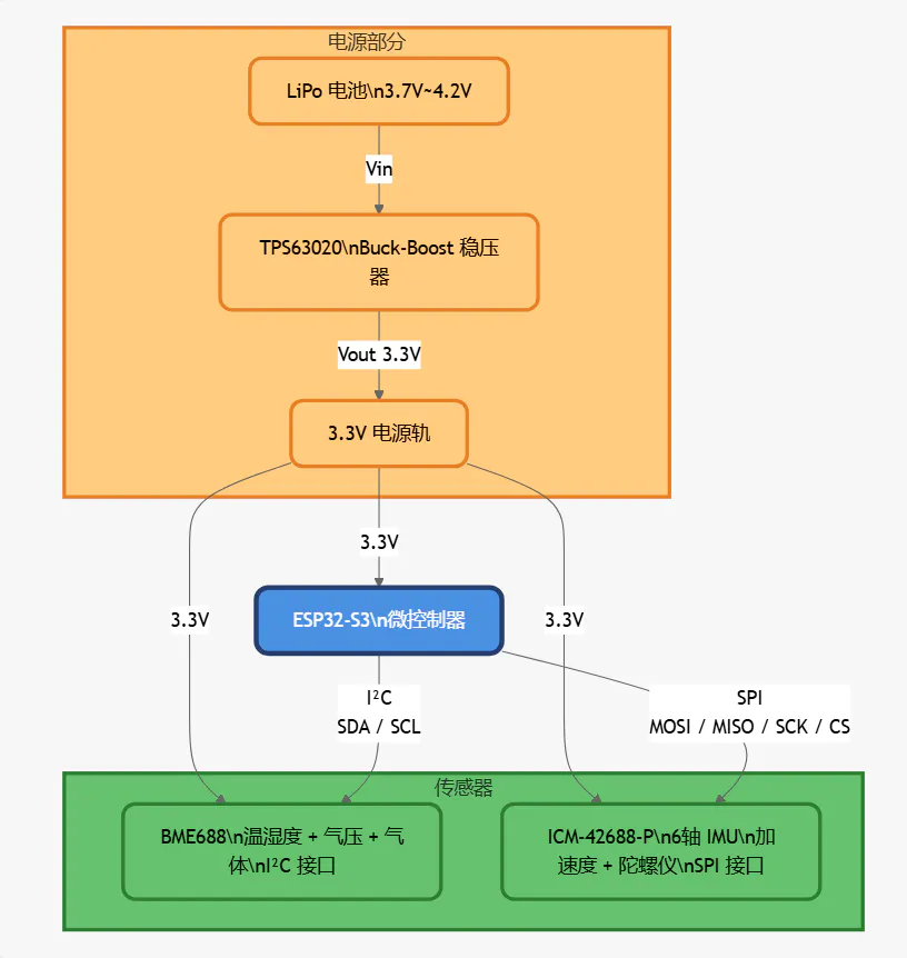
That's exactly the challenge we faced: a compact IoT environmental sensor node designed to fit inside a 32mm diameter cylindrical housing. The main MCU and wireless module needed to sit on a rigid section, while a thin flexible tail connected to a secondary sensor array positioned at a 90-degree angle inside the enclosure. A standard 2-board connector approach would have been unreliable and eaten up too much Z-height. Rigid-flex was the right answer.
In this write-up, we walk through the entire process: stackup design, flex zone layout rules, DFM review, fabrication, and SMT assembly at our facility in Tianjin, China.
Why Rigid-Flex? The Engineering CaseRigid-flex PCBs combine rigid laminate sections (where components are mounted) with flexible polyimide sections (which bend and route between the rigid zones). For this project, the key drivers were:
- Space constraint: The cylindrical enclosure left no room for a wire harness or board-to-board connector stack
- Reliability: Flexible connections outperform ribbon cables under repeated vibration and thermal cycling
- Assembly simplification: One rigid-flex board replaces two separate PCBs plus a connector, reducing BOM and assembly labor
- Signal integrity: Short flex traces between sensors and the MCU reduce noise pickup compared to flying wires
Rigid-flex is typically more expensive than standard FR4, but when you factor in eliminated connectors, reduced assembly labor, and improved MTBF, the total cost of ownership often comes out ahead for volume production.
Step 1 — Stackup DesignRigid Zone (4-Layer):
Layer 1 (Top): Signal + Component pads | 35μm Cu
Layer 2: Ground plane (solid) | 35μm Cu
Layer 3: Power plane (3.3V / 1.8V split) | 35μm Cu
Layer 4 (Bottom): Signal + fanout | 35μm Cu
Flex Zone (2-Layer):
The flex section is a 2-layer polyimide construction. Key material choice: Rolled Annealed (RA) copper is specified instead of electrodeposited (ED) copper. RA copper has a grain structure aligned with the rolling direction, giving it far better flex fatigue resistance.
Step 2 — Flex Zone Layout RulesAll traces run perpendicular to the bend axis. Traces parallel to the bend axis concentrate stress and crack during flexing.
No right-angle bends in the flex zone — all routing uses 45-degree or curved segments.
Traces are fanned out across the full width of the flex zone to distribute mechanical stress evenly.
Minimum bend radius maintained at 3mm for static installation (10x flex thickness per IPC-2223).
No vias in the flex zone. All vias are placed in the rigid sections at least 1mm from the rigid-flex transition boundary.
IPC-2223 Compliance:
- Min bend radius (static): ≥10x flex thickness → Our design: 3mm (20x ✓)
- Conductor spacing in flex: ≥0.1mm → Our design: 0.15mm ✓
- Via-to-flex-boundary clearance: ≥1mm → Our design: 1.2mm ✓
- Coverlay overlap on rigid: ≥0.3mm → Our design: 0.5mm ✓
Three issues were flagged before fabrication:
Issue 1 — Via Too Close to Flex Boundary: A bypass capacitor via was placed 0.7mm from the rigid-flex transition edge, below our 1mm minimum. Relocated 1.5mm inward.
Issue 2 — Trace Width in Flex Zone: Two power traces (3.3V, 150mA) were routed at 0.1mm through the flex zone. Given the thinner 18μm RA copper on flex layers vs. 35μm on rigid, current-carrying capacity is lower. Widened to 0.2mm per IPC-2152.
Issue 3 — Component Too Close to Flex Boundary: A 0402 decoupling capacitor was placed 0.3mm from the transition zone edge. Components this close experience mechanical stress from flex movement. Moved 1.5mm inward.
Step 4 — FabricationRigid-flex fabrication differs from standard FR4 in three key areas:
Layup Sequence: The flex core is fabricated first as a separate sub-assembly, then rigid sections are built up around it using precise registration. Any mis-registration causes trace continuity failures at the transition zone.
Controlled Depth Routing: Rigid sections are routed away from the flex zone using a controlled-depth router — cutting through rigid material only, stopping at the PI layer.
Electrical Testing: All boards received 100% flying probe testing to verify continuity across rigid-to-flex boundaries before shipment.
Lead time: 14 working days for prototype quantity (10 panels).
Step 5 — SMT AssemblyAssembly of rigid-flex boards requires special fixturing. The flex zone cannot run flat through a standard reflow conveyor without risking deformation.
- Custom FR4 carrier fixture fabricated to hold both rigid sections in correct relative orientation
- Stencil thickness: 0.12mm (thinner than standard 0.15mm) to control paste volume on 0201 passives
- AOI after reflow on both rigid sections independently
- First-pass yield: 97.2%
- Wi-Fi connectivity: -78 dBm sensitivity at 10m through one concrete wall
- BME688 readings: Within ±0.3°C and ±1.5% RH vs. calibrated reference
- IMU noise floor: 0.003 dps/√Hz at 25°C
- Rigid-flex continuity after 500 bend cycles (3mm radius): 100% pass
- Board fits within 32mm diameter cylindrical housing with 0.4mm clearance
The rigid-flex design eliminated two board-to-board connectors, reduced total BOM by 8 line items, and enabled a 31% reduction in housing diameter compared to the original 2-board design.
About TJHXPCB
TJHXPCB is a PCB design and assembly manufacturer based in Tianjin, China, providing one-stop services from schematic design to box-build assembly.
If you are designing a rigid-flex board or need a manufacturing partner for a tight-enclosure project, feel free to reach out:
Website: https://tjhxpcb.com/rigid-flex-pcb-design/
Email: contact@tjhxpcb.com
WhatsApp: +86 150 2256 3520


_Ujn5WoVOOu.png?auto=compress%2Cformat&w=40&h=40&fit=fillmax&bg=fff&dpr=2)


Comments