


Hardware components | ||||||
 |
| × | 1 | |||
 |
| × | 1 | |||
Software apps and online services | ||||||
 |
| |||||
Greetings everyone, and welcome back!
Here’s something useful: a DIY buck converter built using the popular LM317 adjustable linear voltage regulator.
We designed a super small module that houses a compact DPAK LM317 IC paired with a few SMD components. The end goal of this module is to power a 64×32 RGB P3 matrix panel.
The idea behind this project came from the need for a more reliable alternative to the commonly used AMS1117. After some research, we came across the LM317, which is widely used in electronic circuits. You’ll often find it inside many devices if you take them apart.
In this project, we developed a demo board/module based on the LM317, and this article covers the complete build process.
MATERIALS REQUIREDThese were the components used in this project—
- Custom PCB
- LM317 DPAK PACKAGE
- 10uF 1206 Capacitors
- 1uF 1206 Capacitors
- 1K Resistor 1206 Package
- 330 Ohms Resistor 1206 Package
- Raspberry Pi PICO
- RGB MATRIX P3 64x32 Panel
- SMPS 240V AC to 12V 5A
- LED 0805 Package
- 10K Resistor 0603 Package
- DIODE SS34
The LM317 is an adjustable linear regulator widely used to derive stable output voltages from a higher DC source. It operates by maintaining a constant 1.25V reference between its output and adjust pins, allowing the output voltage to be precisely set using a pair of external resistors.
It is a three-pin, positive-voltage regulator capable of supplying more than 1.5A over an output voltage range of 1.25V to 37V.
The device requires only two external resistors to set the output voltage and offers excellent performance, with typical line regulation of 0.01% and load regulation of 0.1%.
The LM317 is a highly versatile linear regulator that can be used in numerous applications. It can be configured as a standard voltage regulator, a constant current source for battery charging, a tracking pre-regulator circuit, or even an AC voltage regulator circuit.
It also includes built-in current limiting, thermal overload protection, and safe operating area protection, ensuring reliability even under fault conditions. Overload protection remains functional even if the adjust pin is disconnected. Typically, no capacitors are required unless the device is placed far from the input filter capacitors, in which case an input bypass capacitor is recommended. An optional output capacitor can be added to improve transient response, and bypassing the adjust pin further enhances ripple rejection.
For our circuit, we are using the DPAK (TO-252) footprint, which keeps the design compact while still handling decent power. One of the key advantages of this package is the large exposed tab (internally connected to the output), which can be soldered directly onto a wide copper area on the PCB. This effectively turns the PCB itself into a heatsink, helping dissipate the heat generated due to the voltage drop from 12V to 5V. This approach allows for a clean, space-efficient design without needing bulky external heat sinks while still maintaining good thermal performance.
Check out the Datasheet for more info.
https://www.ti.com/lit/ds/symlink/lm317.pdf
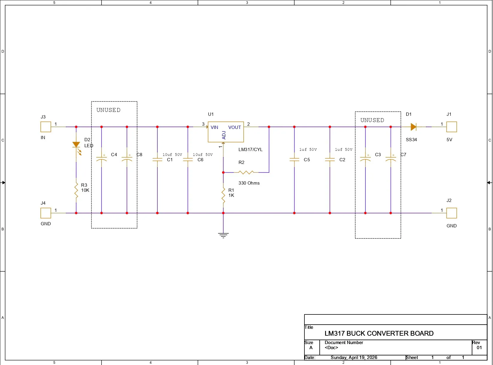
PCB DESIGNWe began the project by preparing the schematic for the buck converter board. We did this by studying the LM317 datasheet and creating a simple schematic that included the LM317 setup with two adjustable resistors connected between the adjust pin and the output pin of the LM317. To ensure stability and reduce noise, we added a 10µF SMD capacitor at the input and a 1µF capacitor at the output, which helps smooth fluctuations and improve transient response. We also added extra capacitor footprints at both the input and output in case different-value capacitors are needed later. The output voltage is configured using a resistor divider (330Ω and 1kΩ), which sets the desired voltage reliably.
After finalizing the PCB schematic, we exported the data and converted it into a PCB layout. The PCB editing process began by adding all the components to the PCB design first. We used all SMD components for this project, including 1206 package capacitors, 1206 package resistors, and a DPAK (TO-252) LM317. We prepared a small board of size 20mm x 30mm and placed all the components within this board. We added four CON1 terminals for the VIN, VOUT, and GND pins, placing them along the edges of the board outline. Two CON1 pads were placed on the right side for the input, and two CON1 pads were placed on the left side for the output.
After finishing the placement, we connected all the net lines and completed the board layout.
After finalizing the PCB design, we exported the Gerber files along with the NC drill files and shared them with NextPCB to get the samples manufactured.
NextPCB PCB SERVICEAfter completing the PCB design, Gerber data for the PCB was sent to HQ NextPCB, and an order was placed for Blue Solder mask boards with a white silkscreen.
After placing the order, the PCBs were received within a week, and the PCB quality was pretty great.
In addition, I have to bring in HQDFM to you, which helped me a lot through many projects. Huaqiu’s in-house engineers developed the free Design for Manufacturing software, HQDFM, revolutionizing how PCB designers visualize and verify their designs.
Take advantage of NextPCB's Accelerator campaign and get 2 free assembled RP2040-based PCBs for your innovative projects.
https://www.nextpcb.com/blog/rp2040-free-pcba-prototypes-nextpcb-accelerator
This offer covers all costs, including logistics, making it easier and more affordable to bring your ideas to life. SMT services can be expensive, but NextPCB is here to help you overcome that hurdle. Simply share your relevant project, and they'll take care of the rest. Don't miss out on this amazing opportunity to advance your tech creations!
HQDFM: Free Online Gerber Viewer and DFM Analysis ToolAlso, NextPCB has its own Gerber Viewer and DFM analysis software.
Your designs are improved by their HQDFM software (DFM) services. Since I find it annoying to have to wait around for DFM reports from manufacturers, HQDFM is the most efficient method for performing a pre-event self-check.
This is what I see in the online Gerber Viewer. It's decent for a quick look, but not entirely clear. For full functionality—like detailed DFM analysis for PCBA—you’ll need to download the desktop software. The web version only offers a basic DFM report.
With comprehensive Design for Manufacture (DFM) analysis features, HQDFM is a free, sophisticated online PCB Gerber file viewer.
With over 15 years of industry experience, it offers valuable insights into advanced manufacturing processes. If you’re looking for reliable PCB services at a budget-friendly price, HQ NextPCB is definitely worth checking out.
PCB ASSEMBLY- We begin the PCB assembly process by first adding solder paste to each component’s pads one by one using a solder paste dispensing needle. Here, we are using 63/37 SnPb solder paste.
- We then pick and place each SMD component in its correct location.
- The PCB is then placed on a reflow hotplate, which heats the PCB from below up to the solder paste melting temperature. As soon as the PCB reaches that temperature, the solder paste melts, and all components are secured in their positions, completing the PCB assembly process.
For the initial test of our buck converter, we used a 240V AC to 12V, 5A SMPS as the power source. We connected the VIN and GND of our buck converter to the 12V output of the SMPS.
Please note that we are working with AC here, so it is recommended to follow proper safety precautions and wear safety gear, such as gloves, while handling AC power.
Using a multimeter, we first measured the voltage across the AC input terminals to ensure that an AC voltage was present at the input of the SMPS.
Next, we measured the voltage across the input of the buck converter, which was around 12V.
Finally, we measured the voltage across the output of the buck converter, which was around 5V. This confirms that our setup is functioning correctly.
Raspberry Pi PICO & RGB P3 Matrix DEMOThe next test for our buck module was a practical application.
We are working with an RGB 64×32 P3 matrix board, which requires a stable 5V, 3A supply, and this setup is driven by a Raspberry Pi Pico and is running our ported version of Conway’s Game of Life, which was perfect for the demo run.
You can check out the article below for a complete breakdown of how to use this matrix panel.
https://www.hackster.io/Arnov_Sharma_makes/64x32-matrix-panel-setup-with-pico-2-25a3c3
CODE
#include <Adafruit_Protomatter.h>
// Pin definitions
#define R1 2
#define G1 3
#define B1 4
#define R2 5
#define G2 8
#define B2 9
#define A 10
#define B 16
#define C 18
#define D 20
#define CLK 11
#define LAT 12
#define OE 13
#define WIDTH 64
#define HEIGHT 32
uint8_t rgbPins[] = { R1, G1, B1, R2, G2, B2 };
uint8_t addrPins[] = { A, B, C, D };
Adafruit_Protomatter matrix(WIDTH, HEIGHT, 1, rgbPins, 4, addrPins, CLK, LAT, OE, false);
bool grid[WIDTH][HEIGHT];
bool newGrid[WIDTH][HEIGHT];
void setup() {
matrix.begin();
randomSeed(analogRead(0));
// Initialize grid with random values
for(int x = 0; x < WIDTH; x++) {
for(int y = 0; y < HEIGHT; y++) {
grid[x][y] = random(2);
}
}
}
void loop() {
matrix.fillScreen(0);
// Update grid based on Game of Life rules
for(int x = 0; x < WIDTH; x++) {
for(int y = 0; y < HEIGHT; y++) {
int aliveNeighbors = countAliveNeighbors(x, y);
if(grid[x][y]) {
// Any live cell with two or three live neighbors survives.
if(aliveNeighbors < 2 || aliveNeighbors > 3) {
newGrid[x][y] = false;
} else {
newGrid[x][y] = true;
}
} else {
// Any dead cell with three live neighbors becomes a live cell.
if(aliveNeighbors == 3) {
newGrid[x][y] = true;
} else {
newGrid[x][y] = false;
}
}
if(newGrid[x][y]) {
matrix.drawPixel(x, y, matrix.color565(255, 255, 255)); // White color
}
}
}
// Copy newGrid to grid
memcpy(grid, newGrid, sizeof(grid));
matrix.show();
delay(100); // Adjust the delay for speed control
// Check if the grid is stable or empty
if(isGridStableOrEmpty()) {
resetGrid();
}
}
int countAliveNeighbors(int x, int y) {
int aliveNeighbors = 0;
for(int dx = -1; dx <= 1; dx++) {
for(int dy = -1; dy <= 1; dy++) {
if(dx == 0 && dy == 0) continue;
int nx = (x + dx + WIDTH) % WIDTH;
int ny = (y + dy + HEIGHT) % HEIGHT;
if(grid[nx][ny]) {
aliveNeighbors++;
}
}
}
return aliveNeighbors;
}
bool isGridStableOrEmpty() {
for(int x = 0; x < WIDTH; x++) {
for(int y = 0; y < HEIGHT; y++) {
if(grid[x][y]) {
return false;
}
}
}
return true;
}
void resetGrid() {
for(int x = 0; x < WIDTH; x++) {
for(int y = 0; y < HEIGHT; y++) {
grid[x][y] = random(2);
}
}
}
After flashing the Pico with the above code, we connected the matrix’s VCC and GND to the VOUT and GND of the LM317 buck converter board. We then turned on the SMPS, and the setup started functioning successfully.
CONCLUSIONThe conclusion of this build is simple: our LM317 buck converter works quite well and can be used with the matrix setup we tested. Not just the matrix, the output voltage of the board can be easily adjusted by changing the values of R1 and R2, allowing it to be used with a variety of applications. For now, we will be using this board in a display-related project and also in a Raspberry Pi 4–based project, which we will be posting shortly.
With that, the project has been finalized, and all the related documents are attached in this article.
Thanks again for reading this far, and peace out!


Comments