


Hardware components | ||||||
| × | 1 | ||||
Software apps and online services | ||||||
| ||||||
| ||||||
| ||||||
| ||||||
I recently began working with the AUP-ZU3 (Zynq UltraScale+) from Xilinx FPGA development board and successfully implemented hardware design by creating and integrating a custom IP core for LED blinking.
The goal of this project was not just to blink an LED, but to understand the full FPGA design workflow, including custom IP creation, system integration, and hardware validation.
This project demonstrates how to:
- Design a hardware module in Verilog
- Package it as a reusable custom IP core
- Integrate it into a Vivado Block Design
- Deploy it on real FPGA hardware
This approach mirrors real-world FPGA system design, where reusable IP blocks are the foundation of scalable architectures.
What I Did1. Designed a parameterized LED blink module in Verilog
2. Packaged the module as a custom IP core using Vivado IP Packager
3. Integrated the IP into a Vivado Block Design
4. Connected the IP to the Zynq Processing System (PS) for clocking
5. Generated the bitstream
6. Programmed the AUP-ZU3 FPGA board
7. Verified LED blinking on hardware by running bitstream on the board
MethodologyCustom IP DesignFolder Structure
The IP:
- Accepts a clock input from the system
- Uses a counter-based approach to divide the clock frequency
- Toggles the LED output at a visible rate
This design was then packaged into a reusable IP block, enabling it to be easily integrated into larger FPGA systems in the future.
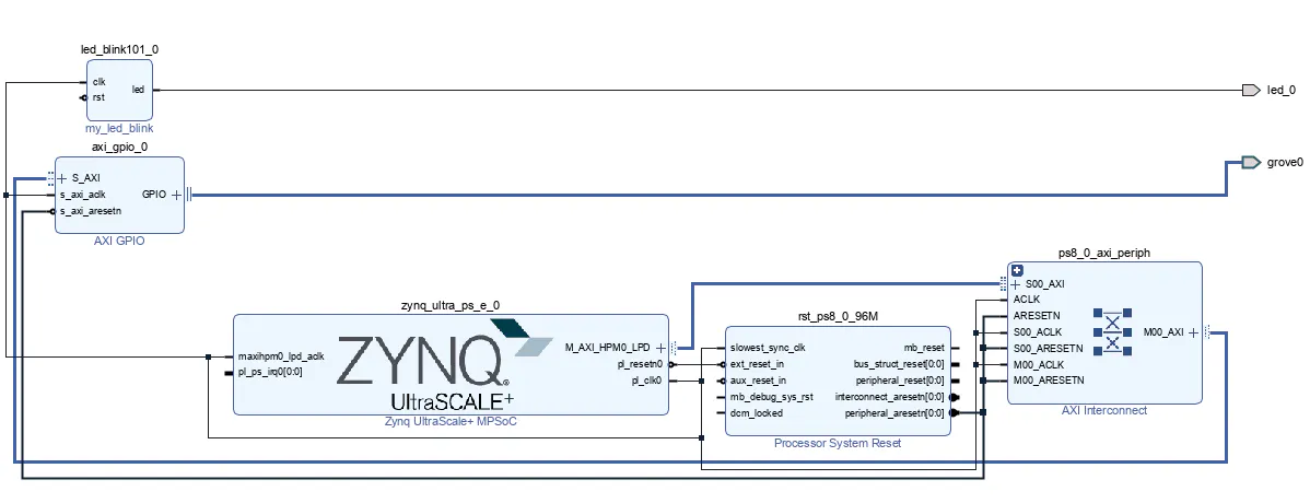
System IntegrationThe custom IP was integrated into a Vivado Block Design alongside the Zynq UltraScale+ Processing System.
This project introduced several important FPGA design concepts:
Custom IP Development: Creating reusable hardware modules for scalable systems
Timing Behavior: Ensuring the design meets clock timing requirements
Hardware Mapping: Connecting internal logic to external physical devices
Key integration points:
The Processing System provides the clock (PL clock)
The custom IP consumes the clock and generates the LED signal
The LED output is mapped to a physical FPGA pin via constraints
Challenges and Lessons LearnedOne of the main challenges was resolving Vivado DRC errors related to unconstrained I/O ports. Initially, the LED output (led_0) was not mapped to a physical pin, which prevented successful bitstream generation.
This was resolved by creating a constraint file (.xdc) and correctly assigning the LED to the appropriate FPGA package pin and I/O standard.
Another important lesson was understanding system-level behavior in Zynq devices. Since the design relies on the Processing System to provide the clock, the PS must be initialized for the Programmable Logic to function correctly.
These challenges provided valuable insight into:
FPGA pin mapping
- FPGA pin mapping
IP integration
Clocking dependencies in Zynq systems
- Results
After resolving integration and constraint issues, the design was successfully deployed to hardware.
The LED on the AUP-ZU3 board blinked as expected, confirming:
- Correct functionality of the custom IP
- Successful integration with the Processing System
- Proper constraint configuration
This project serves as a foundation for more advanced FPGA-based systems. Planned next steps include:
Extending the custom IP to control multiple LEDs
Adding AXI interfaces for processor-controlled operation
Interfacing push buttons and external peripheralsImplementing PWM-based LED dimmingDeveloping hardware accelerators for real-time applications
ConclusionThis project successfully demonstrates the creation, packaging, and deployment of a custom FPGA IP core on the AUP-ZU3 platform.
It represents an important first step toward building more complex, modular, and high-performance FPGA systems using reusable IP-based design methodologies.
This work is part of a broader effort to develop FPGA-accelerated embedded systems for real-time applications such as robotics, perception, and intelligent transportation.
Media (to include)Implemented Device view
- Verilog source code


Comments