

Software apps and online services | ||||||
_4YUDWziWQ8.png?auto=compress%2Cformat&w=48&h=48&fit=fill&bg=ffffff) |
| |||||
| ||||||
| ||||||
Since I was going deep down on black magic field of software stuffs, I was missing to tickle some resistors to blinky a LED. In my research for what other people was doing, I found about artistic PCBs like Badgelife and SAOS. That was interesting to me because at college I used to work a little bit with graphic design. Adding to that, since ever I was inspired by a photo that I took from a friend of mine:
It looks like she is worry-free, weightless and at peace with herself, but still looking for something, and believing that astral energy wield upon her path. Thus, I've got a eureka moment and decided to made this project happen.
Below is a 4-minute video that I've made with care.
In this article I do not want to cover the specifics, which you can see and read in my code and schemas, but some points that I did not cover in GitHub neither on the video before.
Tip No. 1 - About the figureBecause I have already drawn and vectored, the drawing part of the video is a lie, unfortunately. But do not worry, the drawing part existed, but not so simple as shown.
I am not professional, so my way of working is quite crazy: at Gimp, I prepared the photo at the point that can imagine the outline, print it, and work with pencil and eraser. Below I describe its every single step.
1 - Use Crop and Rotate Tools to adjust the figure that you want to work on;
2 - Duplicate the layer. On the top one, apply Filters -> Enhance -> High Pass, and adjust Std. Dev. to a higher value like 20. On layers tab at left, change the mode of the top layer (that turned to gray) to overlay, and then merge down. Maybe you can notice that the figure got less blurred;
3 - Apply Filters -> Edge-Detect -> Edge;
4 - Go to Colours -> Hue-Saturation and set Saturation value to -100;
5 - Apply Colours -> Invert;
6 - Go to Colours -> Levels and set mid tones to higher values;
7 - Print the figure and with pencil and eraser discover the silhouette of the figure. Put in your mind that you will work on PCB, so you have limited resource of colours, space and even details like narrow edges. In this part you probably will go back and forth until define the best format to put on your PCB;
8 - Scan and then vector it. In my case, I used Gimp again to do it.
This is the way that I have worked. But you can skip some of those steps, or even do none of them and reach directly to the vectored image.
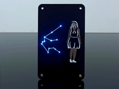
In this figure I have decided that the hair, the cloth and trainers will be in silk screen, and the face, arms and legs will be shown in ENIG. There is the Aquarius constellation too that will be traced in silk screen.
Before working on the figure at Kicad, I have detached the ENIG part away from silk screen. In this way, when calling Kicad's Bitmap to Component Converter, the part that should be silk screen and ENIG would not mixed up.
And when at Kicad's Footprint Editor, the parts can be gathered by moving them.
To transform the part that should be ENIG into a PAD, just add a pad above the part in question, select both parts and right click on them. Select "Create Pad From Selected Shapes", as shown below.
If you are unsure about the microcontroller that you will use, there is not so many projects using them, or/and this type of development is new to you, make a Proof-Of-Concept (POC) first making the desired circuit on a breadboard. Here I have decided to use Tiva TM4c123 development board because I am more familiar with and I like it. I just tested if it was possible to control over 13 PWM signals (it is possible up to 16 for other constellations) and adjust the intensity and frequency of them by adjusting potentiometers.
Long story short, after drawing the schematic and the board, I have obtained a PCB frame in the way I wanted. The potentiometers from breadboard turned into trimpots, assuming that the friend will adjust it only maybe once and could bring to the places without deregulate unintentionally.
In the end the bill of materials was not so pleasant. If you are looking to make a similar project, look for LED1202, I believe that it will cut the cost below the half. I did not used it because I was in the stage of routing the PCB when STMicroelectronics announced that component, and did not wanted to delay the project anymore.
And of course, I made some few mistakes at the first version. And expecting that, I made two options of supply (TPS797 and TPS736) and it could be chosen via pad jumpers just to evaluate which one I should pick up at the final version (I chose the last one in the end).
As I said before about editing on Gimp, I am not professional on making video neither. But I want to raise a couple of points about it.
- For videos with "making of" style, do not decide to make it near the end. Its time consuming to just simulate all the things you have already done. If decided from the start, record all the things as possible, even in uncomfortable angles. At the end you will have a lot of material and speeding up the monotonous part will be interesting.
- Even you made a well explained video or article, maybe people will not see your project because of variety of social media platforms. So take good photos, make a demonstration video of just few seconds, make a gif of some part, and in this way you will have a variety of materials for a variety of media platforms.
Depending on the project, you can even make a very short trailer to attract people attention before releasing the main video. It is up to you, creativity is limitless.
ConclusionMaybe some of you is curious if I really delivered the gift to my friend, and the answer is yes. She loved it. She was so impressed that we exchanged ideas for hours about it and its implications. And not only her, some friends of mine was more impressed about the video I made, and showed interest to make similar project or even adopt tools like Kicad. For me it is very satisfying that I can encourage people in this way.

_Ujn5WoVOOu.png?auto=compress%2Cformat&w=40&h=40&fit=fillmax&bg=fff&dpr=2)

Comments