


When designing a transimpedance amplifier under such narrow restrictions, there are many considerations in the design methodology of the circuit. There are many different topologies for a transimpedance amplifier (TIA) and they all have their own advantages and disadvantages. The simplest form that we think of intuitively is a simple resistive front end, in which the input current is simply imposed over a large resistor. Of course, this type of design has abysmal noise and bandwidth performance. However, this demonstrates the idea of transimpedance amplifiers and why their gain is denoted as a resistance that equates to the ratio of the output voltage to the input current, and is measured in ohms. However there are other common active topologies with better performance in terms of gain, bandwidth, noise etc. One of the most common is a simple common gate amplifier discussed by Razavi (1). In this configuration the input current is imposed at the source of the amplifier over the source load and creates an input voltage at the source of the CG amplifier which is translated to an output voltage. Another fairly common topology is a common source amplifier with resistive feedback (2). This design has the advantages of lowered input impedance and high bandwidth. For this project, the challenges of high transimpedance gain, low noise, and high bandwidth are further strained by the need to drive a differential output load with very low impedence. This motivates the consideration of other differential topologies to achieve high gain and high output swing, like multistage differential configurations (3). To design a TIA that accommodates all the design restrictions, using a combination of these topologies will prove very useful, so long as the tradeoffs between gain, bandwidth, power, and noise are kept closely in mind.
2. Process Characterization- ID vs. VDS for 0
W = 5um (N0), W = 10um (N1), W = 20um (N8), W = 40um (N9), and W = 80um (N10)
Figure 2.1: Schematic for process characterization of Ids v. Vds
Figure 2.2: Simulation results for Ids v Vds of devices with various widths
Figure 2.3: Hand calculations for Ids v. Vds
Comparing Figure 2.3 and Figure 2.2, the results for this process characterization are fairly consistent with my hand calculations. We see that for a given Vgs (1.0V for this test) as Vds increases from zero the devices turn on and enter the triode region of operation and Ids increases exponentially, then once they enter saturation Ids begins to level off. The reason for the slight positive slope of Ids in the saturation as seen in the results in Figure 2.2 and predicted in Figure 2.3 that because of the effect of channel length modulation, Ids will increase gradually as Vds increases. Of course, drain current is proportional to the aspect ratio of the device and therefore for larger values of W, the drain current will be larger yet still follow the same overall behavior as Vds increases. The discrepancies between the hand calculations and the results are largely due to the fact that Cadence uses more advanced parameters than unCox and lambda to calculate the drain current.
- Vth vs Id for 0 < Id < 20mA
W = 5um (N0), W = 10um (N1), W = 20um (N8), W = 40um (N9), and W = 80um (N10)
Figure 2.4: Schematic for the process characterization of Vth vs Id and gm vs. Id and process ft
Figure 2.5: Simulation results for Vth vs Id
Figure 2.6: Hand calculations for Vth v Ids
When comparing Figure 2.6 and Figure 2.5, according to my hand calculations for Vth, I found Vth to be solely depended on the width W of the device an independent of the drain current. However, the results of this characterization tell a different story. For Ids < ~3mA, there seems to be a quick and drastic change in Vth. This may be due to the fact that for most of the devices, the threshold voltage changes as the device Vds increases but when the device is in saturation the Vth remains relatively constant. And as shown in the hand calculations and seen in the results, the Vth is inversely proportional to the device aspect ratio and step-wise decreases for larger values of W.
- gm vs. Id for 0 < Id < 20mA
W = 5um (N0), W = 10um (N1), W = 20um (N8), W = 40um (N9), and W = 80um (N10)
Figure 2.7: Simulation results for gm vs. Ids
Figure 2.8: Hand calculations for gm vs. Ids
As seen in Figure 2.7 and Figure 2.8, my hand calculations show that device trans-conductance is directly proportional to the square root of the aspect ratio and drain current, and therefore step-wise increases as for larger values for W. Also as Id increases the trans-conductance should increase radically (due to the square root function) according to my hand calculations. We see both these relationships hold true in the simulation results.
- Cgs and Cgd vs. Id for 4um< W < 400um
Figure 2.9: Schematic for Cgs and Cgd vs. W
Figure 2.10: Simulation results for Cgs (red) and Cgd (blue) vs. W
Figure 2.11: Hand calculations for Cgs and Cgd vs. W
As shown in Figure 2.10 and Figure 2.11, my hand calculations show that Cgs and Cgd are both linearly proportional to width and should increase at a constant rate as width increases. The simulation results how the negative version of this relationship. This discrepancy is just a nuance of the spice matrix that Cadence uses to calculate Cgs and Cgd and so these negative capacitance should be thought of as positive, and therefore in line with my hand calculations
- Process ft
Figure 2.13: Simulation results for process ft vs Ids
Figure 2.14: Hand Calculations for process ft.
As shown in Figure 2.13 and Figure 2.14, my hand calculations ( a simple equation we have previously derived) the process ft is directly proportional the device trans-conductance and inversely proportional to Cgs and Cgd. However since Cgs and Cgd increase with device width, the process ft should step-wise increase for each larger value of W. Also, the trans-conductance is directly proportional to the square root of the drain current and therefore as Id increases the process ft should increase radically. Again because of the nuance of Cadence calculations for Cgs and Cgd, the results show the negative of what the hand calculations predict.
3. Design StrategyAfter considering the different topologies and strategies to achieve high gain, high bandwidth, low noise, and high output voltage swing, all while maintain low power I decided on the following design:
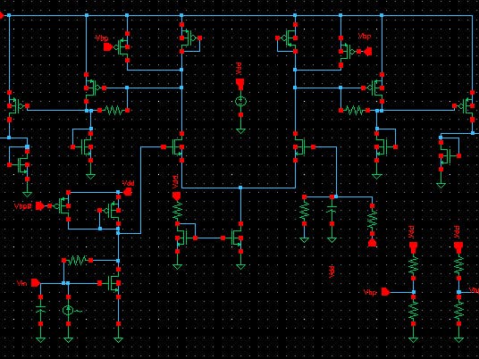
Figure 3.1: TIA schematic with 4 stages: 1st, 2nd (differential), 3rd (+/-), 4th (+/-)
My design uses a multistage cascade design in which each of the 4 stages accomplishes a unique goal. The first stage is a transimpedance stage with moderate gain. I decided on the common source with negative feedback topology because of its advantages in terms of bandwidth extension, when compared to other Common Gate topologies. It also does not require any additional DC biasing and thus does not require a Cbig (DC blocking capacitor). This stage uses a PMOS diode connected load in parallel with a PMOS current source. This implementation (suggested in Razavi) the advantage of a diode load which is beneficial for bandwidth. However in order to maintain reasonable gain, the idea is to “lower the gm of the diode load” by lowering the current through it rather than decreasing its width. To maintain the same current through the main transistor of this stage, the majority of its current will be supplied by the current source in parallel with the load resistance. This topology has the advantages of higher bandwidth, lower noise, solid gain and low headspace consumption when compared to ideal resistors.
The 2nd stage is perfectly symmetric differential amplifier with high gain (using the diode load in parallel with a current source strategy as a drain load listed above). It is designed to operate off the DC bias point of the drain of the previous stage (as are the 3rd and 4th stages) and thus requires no further DC biasing. The 3rd stage is another high gain stage that uses the PMOS common source with resistive feedback topology. It is important to note that while this stage is not true differential pair, this stage on the positive output of stage 2 is perfectly symmetric with stage at the negative output of stage 2 and so their effect on the gain, bandwidth, noise and power can be considered identical on both sides of the differential portion and is referred to as one stage – stage 3(+/-). This stage was added in after testing a 3 stage design (only had 1st, 2nd, and 4th stages) in order for the bandwidth to extend beyond the minimum restriction of 150Mhz. This is because of the restive feedback. This limiting of the gain because of the feedback on a common source voltage amplifier meant that it needed to be added to an additional stage rather than added to the 4th stage. It is necessary for this stage to use PMOS technology so it can utilize the fairly high DC bias point of the previous stage’s drain (~1.8V). Therefore the |Vgs| of this stage would be ~1.2V, not ~1.8V, allowing the drain load to consume enough headspace to offer proper gain and keep the main transistor in saturation.
The 4th and final stage is a differential PMOS common source voltage amplifying stage that accomplishes high output swing. Again although it is not a true differential pair the same considerations of gain, BW etc. in stage 3 are applied. Stage 4 (+/-) has a fairly low voltage gain due to the 300Ω load but can support a high voltage swing and not cut the gain of the previous stages by consuming the most current of all the stages. This is necessary because since the 300Ω load is in parallel with the gain setting the resistor Rd and thus requires a large gm (and therefore high current) of the device. The intricacies of these relationships will be discussed further in the hand calculations. Again due to high DC bias point at the output of the previous stage, this design required PMOS technology so as not to require further DC biasing.
4. Hand Calculations****Full copy of hand calculation attached to the back of the report.
While the majority of the hand calculations are appended to the back of this report, there are some key observations about the general DC calculations, gain, bandwidth and noise of the circuit.
Figure 4.1: Hand calculations for power
Throughout the implementation of this design, it important to keep in mind that the maximum amount of current that this amplifier can consume is 8.33mA according to Figure 4.1. This has implications on the possible size of the transconductance (gm) of each device and thus is a determining factor in how to achieve the necessary transimpedance gain for the circuit.
Figure 4.2: Hand calculations for the transimpedance gain
The gain shown in Figure 4.2 is predominantly determined by the gm of the main transistor in each stage and the drain resistance of each stage, which in practice will be parallel combinations of gm and ro of the respective drain load of each stage. Some other observations include that the feedback resistance of the first stage, Rf1, is directly proportional to the gain of the circuit, but the gm of the first stage can also hinder the overall gain for low values of the drain resistance at stage 1. In general, it seems that high grain resistances and high device transconductance will mean a high transimpedance gain for the overall circuit.
Figure 4.3: Hand calculations for general DC biasing and operating points
Figure 4.3 shows how the gm of a device is directly proportional to the drain current and inversely proportional to the overdrive voltage. Both of these quantities are shown to be proportional to the width of the device. And so, there is a direct tradeoff between width, gm, and drain current. As discussed above, the gain of most of the TIA’s stages are proportional to the gm and drain resistance. However to achieve a high gm, one requires either high current (consuming valuable power), or very low overdrive voltage (which would require a smaller aspect ratio of the device and limits the input swing of that stage to a small range so as to keep the device in saturation). On the other hand, large drain resistances for a considerable current (>~1mA) will take enormous headspace and not allow the main device at its stage to be in saturation. These tradeoffs in power and gain are taken into careful consideration in the design of this amplifier.
Figure 4.4: Hand calculation result for the transfer function of the TIA’s dominant pole
High bandwidth is another primary concern for this design as shown in Figure 4.4 requires a large low-frequency gain, and low equivalent node-to-ground capacitances and resistances. It is important to note that since the dominant pole[s] are heavily dependent on the resistance at that node and so the, tradeoff between bandwidth and gain becomes very apparent. A low resistance at those nodes will limit gain and expand the bandwidth and vice versa. This led to my implementation of the feedback resistor on stage 3. This resistance as shown in the full hand calculations for noise and bandwidth has a minimal effect on the gain of stage 3, but due to the Miller effect it also greatly extends the bandwidth by creating an equivalent resistance to ground. Because both poles C and F share this feedback resistor they should both be considered as part of the transfer function, the truly dominant pole is pole C.
Figure 4.5: Hand calculation results for total input referred current noise.
And lastly Figure 4.5 demonstrates a direct proportionality between device capacitance values, and resistance values. It also demonstrates a clear relationship between noise, gain and bandwidth, and finding a balance to meet the requirements of all such constraints proves to be the biggest challenge in this design.
5. Cadence Simulation Resultsa. DC Operating Point Annotations and Summary Table
Figure 5.0: TIA with annotated component names and DC node voltages
Figure 5.1: DC operating point table
*** It is important to note that only devices N0 & N1, P2 & P3, and P6 & P8 are true differential pairs. All other device pairs referred to as ‘diff pair’ are part of stage 3(+/-) or 4(+/-) and are referred to as ‘diff pairs’ for the sake of brevity.
b. AC simulation from 1kHz to 10GHz
Figure 5.2: AC simulation results
This chart clearly shows the bandwidth of my TIA. Because my design does not utilize a Cbig input DC de-coupling capacitor, nor does it have any large capacitors between any of the stages, this TIA does not have a low corner cutoff frequency. It is also shown that the high corner cut off frequency at the -3dB point is ~172Mhz, which exceeds the minimum bandwidth design restriction
c. Transient Simulation and Stability
Figure 5.3: Transient simulation results
These results show a voltage output swing of 1.91V, exceeding the minimum output swing restriction. We can also see the step response of the circuit in the first few periods of the simulation. It shows the circuit is stable after only 2 periods (~20us)
d. Noise
Figure 5.4: Noise simulation results
These results show the noise over the bandwidth of the circuit as well as the total input referred current noise of 11.25nA
e. Table of Comparison
The simulation results very well reflect the behavior of the circuit described in the hand calculations. Most of the discrepancies are largely due to the advanced modeling parameters that cadence uses for the nmos4 technology and so some standard equations –like the current equation for a device in saturation - may not prove to be all that useful, beyond showing how a designer can modify a design in general to achieve a desired output. However, there are some general discrepancies between my hand calculations and the circuit performance that are worth noting.
First, the gain of stage 1 of this TIA – a common source with resistive feedback transimpedance stage – should be directly proportional and dominated by the value of the feedback resistance Rf1 (shown in hand calculations). In my design, Rf1 has a value of 80kΩ and according to its gain equation, the gain should be extremely high (~50k-60k) for this stage. However, simulation results and testing reveal a transimpedance gain for this stage of about 10k. In addition, parameters like lambda which we use to calculate the ro of a device and equations for the transconductance of a device don’t hold completely true for any given device.
In general, my hand calculations served as a solid starting point for the design of this circuit, and when I had to make decisions on how to increase the gain of the circuit, lower the power or widen the bandwidth.
7. ConclusionThe design of this transimpedence amplifier offered many challenges to which different strategies we employed to overcome. Tight considerations for bandwidth and power make achieving high gain difficult, and so strategies such as adding feedback resistance to a common source stage prove extremely useful. The final results of this 4 stage TIA in some cases exceed the minimum requirements of the design restrictions. This is possible due to the implantation of many strategies and circuit topologies found in the literature research and basic design theories proposed by this course.
8. References1) Design of CMOS Analog Integrated Circuits by Behzad Razavi
2) http://scholar.lib.vt.edu/theses/available/etd-05242013-112845/unrestricted/Ahmed_MN_T_2013.pdf
3) https://mixsignal.files.wordpress.com/2010/04/lecture13_2007.ppt
4) http://www.ece.tamu.edu/~spalermo/ecen474/lecture27_ee474_tias.pdf
5) https://www.wpi.edu/Pubs/ETD/Available/etd-050505-105548/unrestricted/hozbas.pdf
6) http://bwrcs.eecs.berkeley.edu/Classes/EE290C_S04/lectures/Lecture28-Optical.pdf


Comments