


Hardware components | ||||||
 |
| × | 1 | |||
 |
| × | 1 | |||
| × | 1 | ||||
 |
| × | 1 | |||
 |
| × | 1 | |||
 |
| × | 1 | |||
Software apps and online services | ||||||
 |
| |||||
| ||||||
Hand tools and fabrication machines | ||||||
 |
| |||||
 |
| |||||
 |
| |||||
 |
| |||||
 |
| |||||
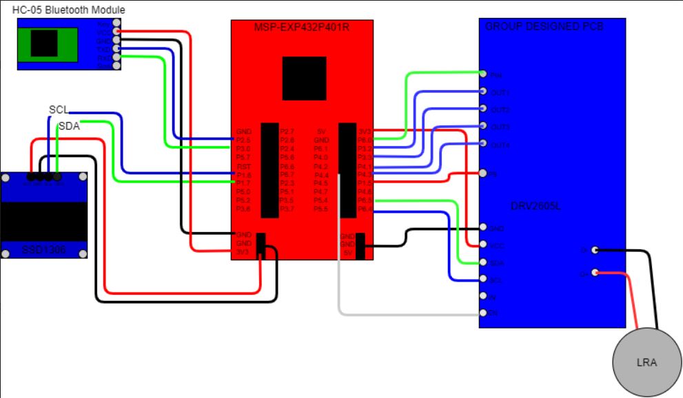
The scope of our project was to be able to combine many different peripherals that can all communicate with each other using the MSP432. For the requirements, we needed to combine several different systems that had to utilize the MSP432, UART Communication, and testing using logic analyzers and the debugger. We used the SSD1306 OLED display to enable user interfacing with the clock, set up alarms. This will be achieved by using a toggle, toggle down, start and menu switch. Using these switches we will be able to determine the mode we want to use, and we will be able to set up alarms and timers using these switches. The menu switch will allows to change the mode that the watch is in. It cycles through all of the modes that the watch will be able to operate on.
To test the project we used logic analyzers to ensure that communication was occuring properly for the I2C and UART drivers. Before testing on an MSP432, we would test the devices with an Arduino Mega, to ensure everything worked properly. We then moved on the MSP432 and wrote basic driver programs that we would use for the larger programs later. We split up roles, set up gantt charts, and worked on the various aspects to ensure completion of the project.
Figure 1: This shows an example of us using the logic analyzer with the Logic 1.2.18 program. Shows the I2C communication between the MSP432 and the OLED display showing that it acknowledges that a signal was received by the device. Below shows the setup.
1. Software for MSP432
For the MSP432, we wrote code that utilized Timer A0 for use in the PWM signals to the piezo buzzer and to increment time on the watch. For the main function, we used switch statements to switch between the various modes and set all of the port 4 pins to receive inputs from the PCB to switch between the various modes.
2. Software for peripherals
We wrote I2C drivers to set the MSP432 as the master and the SSD1306 display as the slave device. We used interrupts routines while communicating between the various devices. For the HC05, we used UART communication to receive data from a smartphone app downloaded off the play store to communicate to the MSP432. We also used I2C drivers when using the DRV2605L to communicate to the LRA.
Theoretical Analysis
Baud Rate/Other Calculations
The baud rate was calculated in this way, using the clock speed, dividing by the baud rate wanted. It was similar done for the SSD1306.
For the clock of the screen, we found that it worked best when the baud rate was the smclk speed divided by 30 as seen in the i2c.c file. This information for both was gotten from the data sheet. The timing of both devices wasn’t an issue as we needed the screen to respond every second and the time was well quicker for transmitting data as seen from the datasheet.
For resistor and capacitor size, we went with 0805 just so it wouldn’t be too much of a hassle to solder onto the boards. For values we just used the max voltage values as a reference and went well below just to be sure. Only real data structure we used for the project was a pointer to a buffer for the screen, which acted similar to a queue, popping out the top when the data was read.
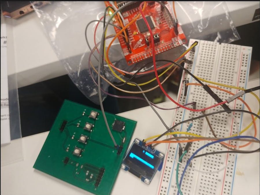
Final PCB
Figure 2: Shown here is the finalized PCB
Our PCB is a 2 layer board consisting of copper and FR4. It was designed to have the Piezo buzzer integrated onto the board (Upper left component). The four buttons that control the watch are seen in the middle of the PCB. This is done by sending a high signal to all four buttons. When a button is pushed, the signal is sent back to the MSP432 where the high signal can be read thus switching the mode that the watch is in, changing the values on the watch clock, or starting and stopping the timer/alarm. The circuit to the right is that of the DRV2605L. Given more time we would be able to include and program for the DRV2605L. This would enable for the alarm to have a tactile alarm along with the audible alarm. Future improvements for this design would be integrating our other boards onto the PCB, and reducing the size of the PCB to make it easier to handle.
Pin Map:
This link shows how the Display cycles between the different modes of the Watch, it shows setting the time for the clock, starting a stopwatch, and setting up an alarm: https://drive.google.com/open?id=1UZxfZivQbGOk21KmBAj91fG-09pu6psY
Debugger
We used the CCS debugger in order to ensure that values were getting set properly in registers to ensure that communication for I2C and UART could occur. We also used it to ensure that the pins were receiving input from the PCB. We used it to debug our project by stepping into functions, stepping over things and seeing where and if the code would get stuck somewhere. It was valuable in helping us figure out where some code was potentially not working. The main use of it for us was the pin inputs for port 4 as we used those to switch between the various modes of the project. Using this allowed us to overcome obstacles if anything wasn’t working to see if the proper registers were being set.
Final Overview
All the devices ended up working out in their respective ways. The SSD1306 had functioning I2C drivers that were able to communicate from the MSP432 and be able to display time, use an alarm and a timer. We were able to communicate with the HC05 Bluetooth module and receive information from it to use. The TimerA0 worked well to create the PWM signals for the piezo buzzer and the LRA. The system of switch statements also worked well to create the menus of different options that the user is able to switch between. We learned a lot throughout this project of how to debug using the logic analyzer when our communication protocols were not working. We learned how to hook it up and learn what the information from the logic analyzer means in terms of receiving data. We learned how to split the work up across the group, writing separate driver functions and bringing them together. We also learned a lot about programming embedded hardware, and utilizing UART and I2C for our various devices. We learned of the limitations of the hardware and how to take that into account when designing our project. We learned how to go through a trade study to pick out our parts and use a gantt chart to ensure things got done in a timely manner. Throughout the project we learned various skills on the way to creating our functioning smart watch.


Comments